EP0724334B2 - Double-sided oscillator package - Google Patents
Double-sided oscillator package Download PDFInfo
- Publication number
- EP0724334B2 EP0724334B2 EP95112907A EP95112907A EP0724334B2 EP 0724334 B2 EP0724334 B2 EP 0724334B2 EP 95112907 A EP95112907 A EP 95112907A EP 95112907 A EP95112907 A EP 95112907A EP 0724334 B2 EP0724334 B2 EP 0724334B2
- Authority
- EP
- European Patent Office
- Prior art keywords
- package
- open
- receptacle
- platform
- piezoelectric element
- Prior art date
- Legal status (The legal status is an assumption and is not a legal conclusion. Google has not performed a legal analysis and makes no representation as to the accuracy of the status listed.)
- Expired - Lifetime
Links
Images

Classifications
-
- H—ELECTRICITY
- H03—ELECTRONIC CIRCUITRY
- H03B—GENERATION OF OSCILLATIONS, DIRECTLY OR BY FREQUENCY-CHANGING, BY CIRCUITS EMPLOYING ACTIVE ELEMENTS WHICH OPERATE IN A NON-SWITCHING MANNER; GENERATION OF NOISE BY SUCH CIRCUITS
- H03B5/00—Generation of oscillations using amplifier with regenerative feedback from output to input
- H03B5/30—Generation of oscillations using amplifier with regenerative feedback from output to input with frequency-determining element being electromechanical resonator
- H03B5/32—Generation of oscillations using amplifier with regenerative feedback from output to input with frequency-determining element being electromechanical resonator being a piezoelectric resonator
-
- H—ELECTRICITY
- H03—ELECTRONIC CIRCUITRY
- H03H—IMPEDANCE NETWORKS, e.g. RESONANT CIRCUITS; RESONATORS
- H03H9/00—Networks comprising electromechanical or electro-acoustic elements; Electromechanical resonators
- H03H9/02—Details
- H03H9/05—Holders or supports
- H03H9/08—Holders with means for regulating temperature
-
- H—ELECTRICITY
- H10—SEMICONDUCTOR DEVICES; ELECTRIC SOLID-STATE DEVICES NOT OTHERWISE PROVIDED FOR
- H10W—GENERIC PACKAGES, INTERCONNECTIONS, CONNECTORS OR OTHER CONSTRUCTIONAL DETAILS OF DEVICES COVERED BY CLASS H10
- H10W74/00—Encapsulations, e.g. protective coatings
-
- H—ELECTRICITY
- H10—SEMICONDUCTOR DEVICES; ELECTRIC SOLID-STATE DEVICES NOT OTHERWISE PROVIDED FOR
- H10W—GENERIC PACKAGES, INTERCONNECTIONS, CONNECTORS OR OTHER CONSTRUCTIONAL DETAILS OF DEVICES COVERED BY CLASS H10
- H10W90/00—Package configurations
Definitions
- the present invention relates generally to frequency control devices and, in particular, to a double-sided oscillator package.
- Frequency control devices are known to include temperature-compensated crystal oscillators (TCXO).
- TCXO temperature-compensated crystal oscillators
- a typical TCXO utilizes a piezoelectric material and temperature compensation circuitry to provide a reliable and stable oscillator output, for example, for high frequency wave forms under varying environmental conditions.
- RF radio frequency
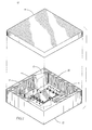
- FIG. 1 is a perspective view of a prior art TCXO 10.
- the TCXO 10 includes a piezoelectric element 12, temperature compensation circuitry in the form of an integrated circuit (IC) 14 and chip capacitors 16, input/output pads (not shown), and a device lid 18.
- IC integrated circuit
- a hermetically sealed environment 20 is formed when the lid 18 and housing 22 are attached.
- the element 12 When a voltage is applied across the piezoelectric element 12, the element 12 resonates at a certain oscillator output.
- the resonant frequency of the piezoelectric element can change or drift about a nominal frequency, responsive to the changes of temperature in the housing 22.
- a temperature sensing device which could be included in the IC provides information to the temperature compensation circuitry regarding the environment 20. As the temperature within the environment 20 fluctuates, the temperature compensation circuitry suitably modifies circuit parameters to minimize frequency drift in the oscillator output.
- the height, width and depth of the TCXO 10 are dependent upon the piezoelectric element, temperature compensation circuitry, integrated circuit 14 and chip capacitors 16 in the housing 22. That is, the overall size of the housing 22 and lid add to the overall dimensions of the TCXO 10. Typical dimensions for the TCXO 10 are about 8.89 mm X 8.89 mm X 2.79 mm.
- Oscillator packages are known e.g. from WO-A-8 912 929 and US-A-4 627 533.
- FIG. 1 is a perspective view of a prior art TCXO.
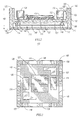
- FIG. 2 shows an enlarged cross-sectional view of a double-sided temperature compensated crystal oscillator package, in accordance with the present invention.
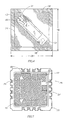
- FIG. 3 shows an enlarged top view of the double-sided oscillator package of FIG. 2, in accordance with the present invention.
- FIG. 4 shows an enlarged bottom view of the double-sided oscillator package of FIG. 2, in accordance with the present invention.
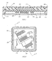
- FIG. 5 shows an enlarged cross-sectional view of an alternate double-sided temperature compensated crystal oscillator package along lines 5-5 in FIG. 8, in accordance with the present invention.
- FIG. 6 shows an upper perspective view showing pockets on a cover of the double-sided oscillator package in FIG. 5, in accordance with the present invention.
- FIG. 7 shows an enlarged top view before placement of an integrated circuit (IC), of the double-sided oscillator package in FIG. 5, in accordance with the present invention.
- IC integrated circuit
- FIG. 8 shows an enlarged bottom view of the double-sided oscillator package with chip capacitors and a piezoelectric element, in accordance with the present invention.
- the present invention provides an improved double-sided temperature compensated crystal oscillator (TCXO) package 100.
- This package 100 includes generally a compensation circuit, having temperature-sensitive components, coupled to a substrate.
- the package 100 is adapted to receive a piezoelectric element mounted onto a portion of the package 100, such that an electrical connection is provided between the compensation circuit and the piezoelectric element to produce an untuned frequency controlled device. After frequency tuning, a hermetic seal is provided around the piezoelectric element.
- FIG. 2 shows the package 100 in its simplest form.
- the package 100 includes a substantially planar platform 102 including a central portion 104, and an outer portion 106. Extending substantially upwardly and downwardly from the outer portion 106 of the platform 102, are upper and lower sidewalls 108 and 110.
- the upper sidewall 108 and the platform 102 form a substantially rectangular, open top receptacle 112 adapted to receive electronic components.
- the lower sidewall 110 and the platform 102 form an open-bottom receptacle 114 adapted to receive at least one piezoelectric component, such as a piezoelectric element 134.
- a cover 116 is attached to the open-bottom receptacle 114 to provide a hermetic environment 118 defined by the open-bottom receptacle 114 and cover 116.
- the platform 102 helps to isolate the receptacles 112 and 114 and components therein, thereby: minimizing the possibility of contamination after assembly or during tuning: and providing a hermetically sealed piezoelectric device 134 which can be processed separately from the electronic components in the open-top receptacle 112, without sacrificing size, integrity or cost. Only one cover 116 is required to achieve this.
- the package 100 geometry can vary widely.
- the package 100 is substantially portable and rectangular or square, and is adapted for placement in an electronic device taking up an extremely small volume of the overall volume of the electronic device.
- the package 100 is particularly adapted for mass production and miniaturization.
- the package can have the dimensions of 7.11 mm x 6.22mm x 2.24mm, identified as the length, width and height 156, 158 and 160 in FIGs. 2 and 4.
- the package 100 comprises materials having substantially similarthermal expansion coefficients, to minimize stresses within the package.
- the open-top receptacle 112 comprises the platform 102 and the upper sidewalls 108 both made of a co-fired ceramic material, such as alumina.
- the lower sidewall 110 can comprise an alloy of nickel, iron and cobalt, Kovar, or Alloy 42, and the like, preferably Kovar because of its coefficient of thermal expansion being substantially similar to the ceramic material making the platform 102 and open-top receptacle 112.
- a plurality of internal leads 120 are included for coupling the electrical components and piezoelectric element 134 to electrical signals for actuating the components in package 100.
- the plurality of leads 120 are coupled to a plurality of respective contacts 124, positioned on an upper-end portion 122.
- the upper-end portion 122 is substantially planar for providing a good contact to a circuit board to which it will be connected.
- the internal leads 120 are formed in the platform 102 and upper sidewalls 108.
- the plurality of conductive leads or paths 120 extend from the central portion 104 to the upper-end portion 122, with each lead being insulated from its adjacent lead.
- the leads 120 provide electrical paths from the circuitry to the end portion 122, and include cofired vias within the ceramic itself, or can include plated half holes, called castellations on the outside of the upper side walls 108.
- the open-top receptacle 112 includes electronic components and the open-bottom receptacle 114 includes at least a piezoelectric element 134. More particularly, the open-top receptacle 112 includes a temperature compensation integrated circuit (IC) 126 and chip capacitors 128 and 130, securely coupled to the central portion 104 of the platform 102.
- the IC 126 can include any suitable IC, for example, a wire bonded IC including a glob top, a flip chip IC including an organic underfill or the like. In a preferred embodiment, the IC 126 is a flip chip IC including an organic underfill 132 for a secure coupling of the IC 126 to the central portion 104 of the platform 102 and for minimizing contamination to the IC 126.
- the IC 126 is solder reflowed onto a metallized portion in proximity to the central portion 104 of the platform. This forms the electrical and mechanical connection of the IC 126 and platform 102.
- the open-top receptacle 112 also includes sufficient space for conductive pads 152 and 154 adapted for tuning the piezoelectric element 134, and first and second chip capacitors 128 and 130 which typically function as DC voltage bypass capacitors.
- the IC 126 itself supplies the temperature compensation function.
- the open-bottom receptacle 114 includes at least the piezoelectric element 134 and can include other components if desired.
- the piezoelectric element 134 can vary widely. Examples can include quartz, AT-cut quartz strip and the like.
- the piezoelectric element 134 comprises an AT-cut quartz strip for a well-behaved frequency versus temperature relationship from about -40°C to about 90°C, that is temperature compensatible. Having the piezoelectric element 134 isolated from the other components minimizes the possibility of contaminating the piezoelectric element 134, resulting in undesirably altering its frequency.
- the cover 116 is complimentary configured to be received and coupled to the open-bottom receptacle 114, and specifically to a lower-end portion 136.
- the cover 116 can be seam welded or solder sealed to the lower sidewalls 110, and preferably to the lower-end portion 136 for providing a good hermetic seal.
- the lower end portion 136 and an outer periphery 138 of cover 116 are complimentary configured to provide a secure interconnection and seal of the contents in the open-bottom receptacle 114 and environment 118.
- the cover 116 is metal and coupled to a ground portion of the IC 126.
- the piezoelectric element 134 is positioned on and coupled to couplings 140 and 142.
- the couplings 140 and 142 provide mechanical and electrical connections to the piezoelectric element 134.
- Electrically connected to the couplings 140 and 142 are leads 144 and 146, preferably in the form of tungsten filled vias, for connecting the piezoelectric element 134 to the circuitry in the open-top receptacle 112 and exterior circuitry, and specifically the IC 126 and capacitors 128 and 130.
- the coupling 140 includes a wraparound section 141 electrically connecting an outwardly facing electrode 164 (top electrode) of the piezoelectric element 134 with lead 144.
- the coupling 142 electrically connects an inwardly facing electrode 162 (bottom electrode facing the platform 102) with lead 146 in FIG. 2.
- the package 100 is suitably coupled to a circuit board for use in an electronic device.
- the planar end portion 122 is configured to facilitate placement on a circuit board or suitable substrate.
- the plurality of contacts 124 are suitably connected to respective leads 120, and to metallized paths on a circuit board for connection to an electrical device.
- Adjacent and perpendicular to the plurality of contacts 124, are respective grooves or castellations 148 on an exterior portion 150 of the upper sidewalls 108.
- these castellations 148 are semicircular for easy inspection of the electrical connections (typically solder) between the contacts 124 to a circuit board.
- the instant invention also includes a method to simplify the coupling of components to packages for use in making oscillators, and is particularly adapted to facilitating mass production of temperature compensated crystal oscillators.
- the instant method of coupling components to a double-sided oscillator package comprises the steps of: providing a package 100 having an open-bottom receptacle 114: mounting and hermetically sealing a piezoelectric element 134 in the open-bottom receptacle 114; and coupling electronic components to the package.
- This method and structure provides an isolation means for minimizing cross-contamination of the components on each side of the package 100. More particularly, the package 100 is configured to substantially minimize contamination from the electronic components in the open-top receptacle 112, such as the IC 126 and capacitors 128 and 130 and associated solder and flux, etc. from the piezoelectric element 134 in the open-bottom receptacle 114. If contamination occurs, the frequency stability of the piezoelectric element 134 can be adversely effected.
- Another advantage of the package 100 and method is that during the process of tuning, typically additional metallization is added to the outwardly facing electrode 164 of the piezoelectric element 134. The possibility of unwanted metal contacting and adversely effecting the components in the open-top receptacle 112 is minimized, because these components are isolated on the other side of platform 102 and typically, have not even been coupled to the package 100 until the tuning step has been completed.
- the method involves: providing a package 100 having an open-top receptacle 112 and an open-bottom receptacle 114; mounting a piezoelectric element 134 in the open-bottom receptacle 114: frequency tuning the piezoelectric element 134; hermetically sealing the piezoelectric element 134 in the open-bottom receptacle 114: and coupling electronic components to the open-top receptacle 112.
- the open-top receptacle 112 includes accessible conductive paths 152 and 154 for actuating the piezoelectric element 134 during the frequency tuning step, whereby metal is added to the outwardly facing electrode 164, for example, before hermetically sealing in the open-bottom receptacle 114.
- the package 100 construction minimizes the possibility of contamination to the IC 126, chip capacitors 128 and 130, and pads 152 and 154 during tuning, since these components are substantially isolated from the piezoelectric element 134 by platform 102 and sidewalls 108 and 110.
- the method relating to make the package 100 in FIGs. 1-4 includes the following:
- the package 200 includes a substantially planar platform 202 including a central portion 204, and an outer portion 206. Extending substantially upwardly and downwardly from the outer portion 206, are upper and lower sidewalls 208 and 210, respectively.
- the upper sidewall 208 and the platform 202 form a substantially rectangular, open-top receptacle 212 adapted to receive at least one electronic component.
- the lower sidewall 210 and the platform 202 form an open-bottom receptacle 214 adapted to receive at least one piezoelectric component, such as a piezoelectric element 234.
- a cover 216 preferably comprising a metal, is attached to the open-bottom receptacle 214 to provide a hermetic environment 218 defined by the open-bottom receptacle 214 and cover 216.
- a curable material 232 is dispensed in the open-top receptacle 212 to substantially cover and enclose the contents therein.
- the platform 202 helps to isolate the receptacles 212 and 214 and components therein, thereby minimizing the possibility of cross-contamination after assembly or during tuning, and providing a hermetic environment 218. Another advantage of this structure, is the integrity, cost benefits and narrow profile.
- This configuration provides one of the smallest TCXO packages on the market, and lends itself to mass production by conveniently separating the piezoelectric element from the IC, and yet only requires one seal requiring leak testing.
- the chip caps are situated with the quartz blank (piezoelectric element), and generally will not impair aging (long term frequency stability). Moreover, this structure takes advantage of the space available inside a square enclosure, to put the chip capacitors appropriately.
- the base adhesive may be the same for the caps as the quartz crystal mount.
- the IC is separated from the hermetic chamber side. A so-called "glob top" epoxy, can be used to substantially protect the wire bonded IC from environmental damage. Applicant is not aware of any prior art TCXO packages which have the structure advantages detailed herein
- a plurality of internal leads 220 are shown for suitably coupling the electrical components and piezoelectric element to electrical signals, for actuating the components in the package 200.
- a plurality of leads 220 are coupled to a plurality of respective contacts 224, positioned on an upper-planar end portion 222.
- the upper end portion 222 is substantially planar for providing a good contact to a circuit board to which it will be connected, for example. This structure is particularly adapted to facilitate surface mounting of the package 200 to a circuit board.
- the internal leads 220 are formed in the platform 202 and upper sidewalls 208.
- the plurality of leads or paths 220 extend from the central portion 204 to the upper-end portion 222, with each lead being insulated from its adjacent lead.
- the leads 220 provide electrical paths from the circuitry to the end portion 222, and can include co-fired vias within the ceramic itself, or can include plated half-holes, sometimes referred to as castellations on the outside of the upper sidewalls 208, for example.
- the open-top receptacle 212 includes at least one electronic component, and similarly, the open-bottom receptacle 214 can include a piezoelectric element 234. More particularly, in FIG. 5 the open-top receptacle 212 includes a wire bonded temperature compensation integrated circuit (IC) 226 suitably connected to various metallizations patterns in receptacle 212, which is coupled to the central portion 204 of the platform 202. In a preferred embodiment, the open-top receptacle 212 is substantially filled with a curable material 232 thus enclosing the IC 226.
- IC wire bonded temperature compensation integrated circuit
- This structure is an efficient configuration from the standpoint of footprint and weight. It allows for example, one to insert the crystal and then seal up the unit so that the IC operation (placement) can be done at a later time, or even at a different location. Even though the hermetic chamber is separated from the IC, there is still only one leak check operation, because the (glob top epoxy) curable material 232 encases the IC and does not have to be leak checked.
- the curable material can vary widely so long as it has a desired viscosity that will substantially homogeneously fill the open-top receptacle 212 when applied, and further when cured, it will substantially be free of bubbles and pockets, which could cause cracks and the like when in use.
- the curable material 232 includes a thermoset, organic, nonconductive material and more preferably includes a material known as Dexter Hysol 4450 which is a glob top epoxy, and can be gotten from Dexter Electronic Materials, 15051 E. Don Julian Rd., Industry, CA 91746.
- a glob top epoxy material provides passivation of the IC. It further provides protection from mechanical damage and is sufficiently moisture resistant to protect the electrical characteristics of the IC.
- the curable material 232 remains below the planar upper-end portion 222, so as not to interfere with the I/O pads or electrical contacts 224 during board reflow.
- the IC 226 is silver epoxied onto a central-metallized portion in proximity to the center portion 104 of the platform 202, to form the appropriate electrical and mechanical connection. After the silver epoxy is cured, the IC can be wire bonded to the metallized areas on the ceramic substrate. These metallized pads are electrically connected to the contacts 224.
- the open-top receptacle 212 also includes conductive pads, such as item 252 for connecting to contacts 224.
- the IC 226 supplies a temperature compensation function appropriate for a temperature compensated crystal oscillator.
- the open-bottom receptacle 214 can include various components.
- the bottom receptacle 214 includes a piezoelectric element 234 and other components, if desired.
- two chip capacitors 228 and 230 are included, which typically function as DC voltage bypass capacitors.
- the piezoelectric element 134 comprises an AT-cut quartz strip, for desirable temperature compensation (TC) characteristics. Placing the piezoelectric element 134 away from the IC, can minimize the possibility of contamination to it, and cross-contamination of the components of the package 200.
- the final tuning of the quartz crystal can be accomplished without the IC encumbering this operation.
- the electrical pads connected to the crystal are located on the opposite side of the crystal chamber, which is advantageous during the final tune operation.
- the cover 216 is complimentarily configured to be received and coupled to the open-bottom receptacle 214, and specifically to a lower-end portion 236.
- the cover 216 is metal, and can be seam-welded or sodder sealed to the lower sidewalls 210, for providing a good hermetic seal.
- the cover 116 can be coupled to a ground portion of the IC 226, for providing a good plane and shielding.
- a metal cover which is connected to the circuit ground, can improve the radio frequency (RF) shielding between the crystal during operation and RF frequencies and the printed circuit board to which the oscillator is bonded on, for example.
- RF radio frequency
- the cover 216 includes pockets 244 for at least partially receiving the chip capacitors 228 and 230, for minimizing the profile of the overall package 200.
- the piezoelectric element 234 is positioned on and coupled through couplings 240 and 242, which provide mechanical and electrical connections.
- the couplings are a conductive compliant material, such as silver epoxy or silver-filled silicone, preferably Emerson & Cumings C990 silver epoxy for good compliance.
- FIGs. 5-8 Much of the structure in the embodiment shown in FIGs. 5-8, is similar to the package in FIGs. 2-4. Thus, the item numbers in the first embodiment (item 100 et seq.) are similar to those in the second embodiment (items 200 et seq.) in FIGs. 5-8.
- the process flow for making the package 200 in FIGs. 5-8 is similar in many respects to that of making the package 100 in FIGs. 2-4. More particularly, it generally includes the following: (1) a double-sided TCXO package as shown in the figures is provided. (2) A silver epoxy is dispensed in a central portion of the open-bottom receptacle 214. (3) The chip caps and quartz crystal are suitably placed in the open-bottom receptacle 214. (4) A silver epoxy is dispensed on a top portion of the crystal for providing a wrap around connection to a central portion 204 of the platform 202. (5) The epoxy is cured by placing the package in an oven for an appropriate period of time.
- the quartz crystal is frequency tuned by mass loading of the crystal, while actuating the quartz crystal through the metal pads.
- the crystal is hermetically sealed with a metal cover, by placing and sealing the metal lid with a seam weld around a periphery thereof.
- a silver epoxy is dispensed at selective positions in the open top receptacle 212.
- the IC is suitably placed in proximity to and over the epoxy.
- the epoxy is then cured.
- the IC is next suitably wire bonded to the appropriate electrical connections in the central portion 204.
- a glob top epoxy is dispensed substantially over the IC.
- the epoxy is cured and the unit is tested.
Landscapes
- Physics & Mathematics (AREA)
- Acoustics & Sound (AREA)
- Oscillators With Electromechanical Resonators (AREA)
- Amplifiers (AREA)
- Control Of Motors That Do Not Use Commutators (AREA)
- Diaphragms For Electromechanical Transducers (AREA)
- Piezo-Electric Or Mechanical Vibrators, Or Delay Or Filter Circuits (AREA)
Abstract
Description
- The present invention relates generally to frequency control devices and, in particular, to a double-sided oscillator package.
- Frequency control devices are known to include temperature-compensated crystal oscillators (TCXO). A typical TCXO utilizes a piezoelectric material and temperature compensation circuitry to provide a reliable and stable oscillator output, for example, for high frequency wave forms under varying environmental conditions. These devices are commonly found in portable radio frequency (RF) communication equipment, such as cellular telephones, pagers and wireless modems. As consumer demand continually drives down the size of cellular telephones and other communications equipment, the need for TCXO's having smaller dimensions and reduced weight has become even greater.
- FIG. 1 is a perspective view of a
prior art TCXO 10. TheTCXO 10 includes apiezoelectric element 12, temperature compensation circuitry in the form of an integrated circuit (IC) 14 andchip capacitors 16, input/output pads (not shown), and adevice lid 18. A hermetically sealedenvironment 20 is formed when thelid 18 andhousing 22 are attached. - When a voltage is applied across the
piezoelectric element 12, theelement 12 resonates at a certain oscillator output. The resonant frequency of the piezoelectric element can change or drift about a nominal frequency, responsive to the changes of temperature in thehousing 22. Typically, a temperature sensing device which could be included in the IC provides information to the temperature compensation circuitry regarding theenvironment 20. As the temperature within theenvironment 20 fluctuates, the temperature compensation circuitry suitably modifies circuit parameters to minimize frequency drift in the oscillator output. - The height, width and depth of the
TCXO 10 are dependent upon the piezoelectric element, temperature compensation circuitry, integratedcircuit 14 andchip capacitors 16 in thehousing 22. That is, the overall size of thehousing 22 and lid add to the overall dimensions of the TCXO 10. Typical dimensions for the TCXO 10 are about 8.89 mm X 8.89 mm X 2.79 mm. - While these dimensions may appear to be small, the demand for smaller cellular telephones and other electronic products necessitates TCXO's having even smaller physical dimensions. Therefore, a substantial need for frequency control devices which overcome prior art dimensional limitations, and which meet or exceed the appropriate performance requirements or criteria of their larger counterparts are needed.
- There is also a need for: (i) a package or housing for frequency control devices which allows the piezoelectric element to be housed separately or to be isolated from the other components without sacrificing space, to minimize the possibility of cross-contamination of the components: and (ii) a mass producable package which can simplify frequency tuning and hermetic sealing.
- Oscillator packages are known e.g. from WO-A-8 912 929 and US-A-4 627 533.
- The present invention is defined by the appended
claim 1, with advantageous embodiments found in dependent claims 2-11. - FIG. 1 is a perspective view of a prior art TCXO.
- FIG. 2 shows an enlarged cross-sectional view of a double-sided temperature compensated crystal oscillator package, in accordance with the present invention.
- FIG. 3 shows an enlarged top view of the double-sided oscillator package of FIG. 2, in accordance with the present invention.
- FIG. 4 shows an enlarged bottom view of the double-sided oscillator package of FIG. 2, in accordance with the present invention.
- FIG. 5 shows an enlarged cross-sectional view of an alternate double-sided temperature compensated crystal oscillator package along lines 5-5 in FIG. 8, in accordance with the present invention.
- FIG. 6 shows an upper perspective view showing pockets on a cover of the double-sided oscillator package in FIG. 5, in accordance with the present invention.
- FIG. 7 shows an enlarged top view before placement of an integrated circuit (IC), of the double-sided oscillator package in FIG. 5, in accordance with the present invention.
- FIG. 8 shows an enlarged bottom view of the double-sided oscillator package with chip capacitors and a piezoelectric element, in accordance with the present invention.
- The present invention provides an improved double-sided temperature compensated crystal oscillator (TCXO)
package 100. Thispackage 100 includes generally a compensation circuit, having temperature-sensitive components, coupled to a substrate. Thepackage 100 is adapted to receive a piezoelectric element mounted onto a portion of thepackage 100, such that an electrical connection is provided between the compensation circuit and the piezoelectric element to produce an untuned frequency controlled device. After frequency tuning, a hermetic seal is provided around the piezoelectric element. With thepackage 100 of this invention, the dimensional limitations of the prior art frequency control devices are substantially overcome. - The present invention can be more fully described with reference to FIGs. 2-4. FIG. 2 shows the
package 100 in its simplest form. Thepackage 100 includes a substantiallyplanar platform 102 including acentral portion 104, and anouter portion 106. Extending substantially upwardly and downwardly from theouter portion 106 of theplatform 102, are upper andlower sidewalls upper sidewall 108 and theplatform 102 form a substantially rectangular,open top receptacle 112 adapted to receive electronic components. Similarly, thelower sidewall 110 and theplatform 102 form an open-bottom receptacle 114 adapted to receive at least one piezoelectric component, such as apiezoelectric element 134. Acover 116 is attached to the open-bottom receptacle 114 to provide ahermetic environment 118 defined by the open-bottom receptacle 114 andcover 116. Theplatform 102 helps to isolate thereceptacles piezoelectric device 134 which can be processed separately from the electronic components in the open-top receptacle 112, without sacrificing size, integrity or cost. Only onecover 116 is required to achieve this. - The
package 100 geometry can vary widely. In one embodiment, thepackage 100 is substantially portable and rectangular or square, and is adapted for placement in an electronic device taking up an extremely small volume of the overall volume of the electronic device. - The
package 100 is particularly adapted for mass production and miniaturization. For example, the package can have the dimensions of 7.11 mm x 6.22mm x 2.24mm, identified as the length, width andheight - In a preferred embodiment, the
package 100 comprises materials having substantially similarthermal expansion coefficients, to minimize stresses within the package. In one embodiment, the open-top receptacle 112 comprises theplatform 102 and theupper sidewalls 108 both made of a co-fired ceramic material, such as alumina. Thelower sidewall 110 can comprise an alloy of nickel, iron and cobalt, Kovar, or Alloy 42, and the like, preferably Kovar because of its coefficient of thermal expansion being substantially similar to the ceramic material making theplatform 102 and open-top receptacle 112. - A plurality of internal leads 120 (shown as dashed lines in FIG. 2) are included for coupling the electrical components and
piezoelectric element 134 to electrical signals for actuating the components inpackage 100. Referring to FIGs. 2 and 3, the plurality ofleads 120 are coupled to a plurality ofrespective contacts 124, positioned on an upper-end portion 122. Preferably, the upper-end portion 122 is substantially planar for providing a good contact to a circuit board to which it will be connected. Theinternal leads 120 are formed in theplatform 102 andupper sidewalls 108. Thus, the plurality of conductive leads orpaths 120 extend from thecentral portion 104 to the upper-end portion 122, with each lead being insulated from its adjacent lead. Theleads 120 provide electrical paths from the circuitry to theend portion 122, and include cofired vias within the ceramic itself, or can include plated half holes, called castellations on the outside of theupper side walls 108. - The open-
top receptacle 112 includes electronic components and the open-bottom receptacle 114 includes at least apiezoelectric element 134. More particularly, the open-top receptacle 112 includes a temperature compensation integrated circuit (IC) 126 andchip capacitors central portion 104 of theplatform 102. The IC 126 can include any suitable IC, for example, a wire bonded IC including a glob top, a flip chip IC including an organic underfill or the like. In a preferred embodiment, the IC 126 is a flip chip IC including anorganic underfill 132 for a secure coupling of the IC 126 to thecentral portion 104 of theplatform 102 and for minimizing contamination to the IC 126. - The IC 126 is solder reflowed onto a metallized portion in proximity to the
central portion 104 of the platform. This forms the electrical and mechanical connection of the IC 126 andplatform 102. - The open-
top receptacle 112 also includes sufficient space forconductive pads piezoelectric element 134, and first andsecond chip capacitors IC 126 itself supplies the temperature compensation function. - The open-
bottom receptacle 114 includes at least thepiezoelectric element 134 and can include other components if desired. Thepiezoelectric element 134 can vary widely. Examples can include quartz, AT-cut quartz strip and the like. In a preferred embodiment, thepiezoelectric element 134 comprises an AT-cut quartz strip for a well-behaved frequency versus temperature relationship from about -40°C to about 90°C, that is temperature compensatible. Having thepiezoelectric element 134 isolated from the other components minimizes the possibility of contaminating thepiezoelectric element 134, resulting in undesirably altering its frequency. - More particularly, isolating and physically separating the
piezoelectric element 134 in the open-bottom receptacle 112 from the components in the open-top receptacle 112, substantially minimizes the possibility of the solder, organic underfill, and other unwanted contaminants from adversely affecting the output frequency of thepiezoelectric element 134, which can occur over time in prior art TCXO's. - The
cover 116 is complimentary configured to be received and coupled to the open-bottom receptacle 114, and specifically to a lower-end portion 136. Thecover 116 can be seam welded or solder sealed to the lower sidewalls 110, and preferably to the lower-end portion 136 for providing a good hermetic seal. - More particularly, the
lower end portion 136 and anouter periphery 138 ofcover 116 are complimentary configured to provide a secure interconnection and seal of the contents in the open-bottom receptacle 114 andenvironment 118. In one embodiment, thecover 116 is metal and coupled to a ground portion of theIC 126. - Referring to FIGs. 2 and 4, the
piezoelectric element 134 is positioned on and coupled tocouplings couplings piezoelectric element 134. Electrically connected to thecouplings leads 144 and 146, preferably in the form of tungsten filled vias, for connecting thepiezoelectric element 134 to the circuitry in the open-top receptacle 112 and exterior circuitry, and specifically theIC 126 andcapacitors coupling 140 includes awraparound section 141 electrically connecting an outwardly facing electrode 164 (top electrode) of thepiezoelectric element 134 withlead 144. Similarly, thecoupling 142 electrically connects an inwardly facing electrode 162 (bottom electrode facing the platform 102) with lead 146 in FIG. 2. - Once the
TCXO package 100 has been assembled, thepackage 100 is suitably coupled to a circuit board for use in an electronic device. Theplanar end portion 122 is configured to facilitate placement on a circuit board or suitable substrate. The plurality ofcontacts 124 are suitably connected torespective leads 120, and to metallized paths on a circuit board for connection to an electrical device. Adjacent and perpendicular to the plurality ofcontacts 124, are respective grooves orcastellations 148 on anexterior portion 150 of theupper sidewalls 108. Preferably, thesecastellations 148 are semicircular for easy inspection of the electrical connections (typically solder) between thecontacts 124 to a circuit board. - The instant invention also includes a method to simplify the coupling of components to packages for use in making oscillators, and is particularly adapted to facilitating mass production of temperature compensated crystal oscillators.
- In its simplest form, the instant method of coupling components to a double-sided oscillator package, comprises the steps of: providing a
package 100 having an open-bottom receptacle 114: mounting and hermetically sealing apiezoelectric element 134 in the open-bottom receptacle 114; and coupling electronic components to the package. - This method and structure provides an isolation means for minimizing cross-contamination of the components on each side of the
package 100. More particularly, thepackage 100 is configured to substantially minimize contamination from the electronic components in the open-top receptacle 112, such as theIC 126 andcapacitors piezoelectric element 134 in the open-bottom receptacle 114. If contamination occurs, the frequency stability of thepiezoelectric element 134 can be adversely effected. - Another advantage of the
package 100 and method is that during the process of tuning, typically additional metallization is added to the outwardly facingelectrode 164 of thepiezoelectric element 134. The possibility of unwanted metal contacting and adversely effecting the components in the open-top receptacle 112 is minimized, because these components are isolated on the other side ofplatform 102 and typically, have not even been coupled to thepackage 100 until the tuning step has been completed. - In a preferred embodiment, the method involves: providing a
package 100 having an open-top receptacle 112 and an open-bottom receptacle 114; mounting apiezoelectric element 134 in the open-bottom receptacle 114: frequency tuning thepiezoelectric element 134; hermetically sealing thepiezoelectric element 134 in the open-bottom receptacle 114: and coupling electronic components to the open-top receptacle 112. - Advantageously, the open-
top receptacle 112 includes accessibleconductive paths piezoelectric element 134 during the frequency tuning step, whereby metal is added to the outwardly facingelectrode 164, for example, before hermetically sealing in the open-bottom receptacle 114. Thepackage 100 construction minimizes the possibility of contamination to theIC 126,chip capacitors pads piezoelectric element 134 byplatform 102 andsidewalls - In a preferred embodiment, the method relating to make the
package 100 in FIGs. 1-4, includes the following: - 1) A double-
sided TCXO package 100 is provided. Thepackage 100 includes a multi-layer ceramic portion defining theupper sidewalls 108 and a metal brazed ring defining the lower sidewalls 110, coupled to theplatform 102. 2) A quartz crystal is placed in the open-bottom receptacle 114 when the package is facing upwardly and is suitably attached to thecentral portion 104. 3) The quartz crystal is frequency tuned by mass loading of the crystal, while actuating the quartz crystal through themetal pads top receptacle 112 in thecentral portion 104 of thepackage 100. 4) The crystal is then hermetically sealed with ametal cover 116 by utilizing a parallel seam weld to couple the lower-edge portion 136 of thelower sidewalls 110 with thecover 116. The crystal portion of the fabrication process is now complete. 5) The electronic components are placed in the open-top receptacle 112 and suitably attached by dispensing solder on theplatform 102 for coupling thechip capacitors IC 126 area. A flip-chip IC with solder bumps is aligned and placed in thecentral portion 104 of theplatform 102. The parts are then solder reflowed. And organic underfill is dispensed such that it flows underneath theIC 126 and substantially environmentally protects theIC 126. 6) Thereafter, theTCXO package 100 is sent for final electrical set up and testing. Thereafter, a customer will typically solder reflow theplanar portion 122 to a circuit board suitably connecting each of thecontacts 124 to a suitable electrical connection for use in electronic equipment. This method can simplify mounting and assembly of components. -
- Referring to FIGs. 5-8, an alternate double sided temperature compensated
crystal oscillator package 200 is shown. Thepackage 200 includes a substantiallyplanar platform 202 including acentral portion 204, and anouter portion 206. Extending substantially upwardly and downwardly from theouter portion 206, are upper andlower sidewalls upper sidewall 208 and theplatform 202 form a substantially rectangular, open-top receptacle 212 adapted to receive at least one electronic component. Similarly, thelower sidewall 210 and theplatform 202 form an open-bottom receptacle 214 adapted to receive at least one piezoelectric component, such as apiezoelectric element 234. Acover 216, preferably comprising a metal, is attached to the open-bottom receptacle 214 to provide ahermetic environment 218 defined by the open-bottom receptacle 214 andcover 216. In a preferred embodiment, acurable material 232 is dispensed in the open-top receptacle 212 to substantially cover and enclose the contents therein. Theplatform 202 helps to isolate thereceptacles hermetic environment 218. Another advantage of this structure, is the integrity, cost benefits and narrow profile. - This configuration provides one of the smallest TCXO packages on the market, and lends itself to mass production by conveniently separating the piezoelectric element from the IC, and yet only requires one seal requiring leak testing. The chip caps are situated with the quartz blank (piezoelectric element), and generally will not impair aging (long term frequency stability). Moreover, this structure takes advantage of the space available inside a square enclosure, to put the chip capacitors appropriately. The base adhesive may be the same for the caps as the quartz crystal mount. The IC is separated from the hermetic chamber side. A so-called "glob top" epoxy, can be used to substantially protect the wire bonded IC from environmental damage. Applicant is not aware of any prior art TCXO packages which have the structure advantages detailed herein
- A plurality of internal leads 220 (shown as dashed lines in FIG. 5) are shown for suitably coupling the electrical components and piezoelectric element to electrical signals, for actuating the components in the
package 200. Thus, a plurality of leads 220 are coupled to a plurality ofrespective contacts 224, positioned on an upper-planar end portion 222. Preferably, theupper end portion 222 is substantially planar for providing a good contact to a circuit board to which it will be connected, for example. This structure is particularly adapted to facilitate surface mounting of thepackage 200 to a circuit board. The internal leads 220 are formed in theplatform 202 andupper sidewalls 208. Thus, the plurality of leads or paths 220 extend from thecentral portion 204 to the upper-end portion 222, with each lead being insulated from its adjacent lead. The leads 220 provide electrical paths from the circuitry to theend portion 222, and can include co-fired vias within the ceramic itself, or can include plated half-holes, sometimes referred to as castellations on the outside of theupper sidewalls 208, for example. - As illustrated in FIG. 5, the open-
top receptacle 212 includes at least one electronic component, and similarly, the open-bottom receptacle 214 can include apiezoelectric element 234. More particularly, in FIG. 5 the open-top receptacle 212 includes a wire bonded temperature compensation integrated circuit (IC) 226 suitably connected to various metallizations patterns inreceptacle 212, which is coupled to thecentral portion 204 of theplatform 202. In a preferred embodiment, the open-top receptacle 212 is substantially filled with acurable material 232 thus enclosing theIC 226. - This structure is an efficient configuration from the standpoint of footprint and weight. It allows for example, one to insert the crystal and then seal up the unit so that the IC operation (placement) can be done at a later time, or even at a different location. Even though the hermetic chamber is separated from the IC, there is still only one leak check operation, because the (glob top epoxy)
curable material 232 encases the IC and does not have to be leak checked. - The curable material can vary widely so long as it has a desired viscosity that will substantially homogeneously fill the open-
top receptacle 212 when applied, and further when cured, it will substantially be free of bubbles and pockets, which could cause cracks and the like when in use. In a preferred embodiment, thecurable material 232 includes a thermoset, organic, nonconductive material and more preferably includes a material known as Dexter Hysol 4450 which is a glob top epoxy, and can be gotten from Dexter Electronic Materials, 15051 E. Don Julian Rd., Industry, CA 91746. - A glob top epoxy material, provides passivation of the IC. It further provides protection from mechanical damage and is sufficiently moisture resistant to protect the electrical characteristics of the IC. Advantageously, the
curable material 232 remains below the planar upper-end portion 222, so as not to interfere with the I/O pads orelectrical contacts 224 during board reflow. - In a preferred embodiment, the
IC 226 is silver epoxied onto a central-metallized portion in proximity to thecenter portion 104 of theplatform 202, to form the appropriate electrical and mechanical connection. After the silver epoxy is cured, the IC can be wire bonded to the metallized areas on the ceramic substrate. These metallized pads are electrically connected to thecontacts 224. - The open-
top receptacle 212 also includes conductive pads, such asitem 252 for connecting tocontacts 224. TheIC 226 supplies a temperature compensation function appropriate for a temperature compensated crystal oscillator. - The open-
bottom receptacle 214 can include various components. In a preferred embodiment, thebottom receptacle 214 includes apiezoelectric element 234 and other components, if desired. Preferably, twochip capacitors piezoelectric element 134 comprises an AT-cut quartz strip, for desirable temperature compensation (TC) characteristics. Placing thepiezoelectric element 134 away from the IC, can minimize the possibility of contamination to it, and cross-contamination of the components of thepackage 200. - Advantageously, the final tuning of the quartz crystal can be accomplished without the IC encumbering this operation. The electrical pads connected to the crystal are located on the opposite side of the crystal chamber, which is advantageous during the final tune operation.
- As shown in FIGs. 5 and 6, the
cover 216 is complimentarily configured to be received and coupled to the open-bottom receptacle 214, and specifically to a lower-end portion 236. In a preferred embodiment, thecover 216 is metal, and can be seam-welded or sodder sealed to the lower sidewalls 210, for providing a good hermetic seal. When metal, thecover 116 can be coupled to a ground portion of theIC 226, for providing a good plane and shielding. A metal cover which is connected to the circuit ground, can improve the radio frequency (RF) shielding between the crystal during operation and RF frequencies and the printed circuit board to which the oscillator is bonded on, for example. - In one embodiment, the
cover 216 includespockets 244 for at least partially receiving thechip capacitors overall package 200. - Referring to FIG. 5, the
piezoelectric element 234 is positioned on and coupled throughcouplings 240 and 242, which provide mechanical and electrical connections. The couplings are a conductive compliant material, such as silver epoxy or silver-filled silicone, preferably Emerson & Cumings C990 silver epoxy for good compliance. - Much of the structure in the embodiment shown in FIGs. 5-8, is similar to the package in FIGs. 2-4. Thus, the item numbers in the first embodiment (
item 100 et seq.) are similar to those in the second embodiment (items 200 et seq.) in FIGs. 5-8. - The process flow for making the
package 200 in FIGs. 5-8, is similar in many respects to that of making thepackage 100 in FIGs. 2-4. More particularly, it generally includes the following: (1) a double-sided TCXO package as shown in the figures is provided. (2) A silver epoxy is dispensed in a central portion of the open-bottom receptacle 214. (3) The chip caps and quartz crystal are suitably placed in the open-bottom receptacle 214. (4) A silver epoxy is dispensed on a top portion of the crystal for providing a wrap around connection to acentral portion 204 of theplatform 202. (5) The epoxy is cured by placing the package in an oven for an appropriate period of time. (6) The quartz crystal is frequency tuned by mass loading of the crystal, while actuating the quartz crystal through the metal pads. (7) The crystal is hermetically sealed with a metal cover, by placing and sealing the metal lid with a seam weld around a periphery thereof. (8) Next, a silver epoxy is dispensed at selective positions in the opentop receptacle 212. (9) The IC is suitably placed in proximity to and over the epoxy. (10) The epoxy is then cured. (11) The IC is next suitably wire bonded to the appropriate electrical connections in thecentral portion 204. (12) A glob top epoxy is dispensed substantially over the IC. (13) The epoxy is cured and the unit is tested. - Although the present invention has been described with reference to certain preferred embodiments, numerous modifications and variations can be made by those skilled in the art without departing from the scope of this invention as defined by the appended claims.
Claims (11)
- A double-sided temperature compensated oscillator package (100) including a platform (102) having a central portion (104) and an outer portion (106), comprising:sidewalls (108, 110) extending substantially upwardly and substantially downwardly from the outer portion (106) of the platform (102),the upwardly extending sidewalls (108) terminating at a surface mountable end portion (122), the surface mountable end portion (122) including a plurality of integral contacts (124) adapted to facilitate electrical surface mountable connection to an electrical device;the upwardly extending sidewalls (108) and the platform (102) forming an open-top receptacle (112) adapted to receive and electrically connect at least one electronic component andthe downwardly extending sidewalls (110) and the platform (102) forming an open-bottom receptacle (114) adapted to receive and electrically connect at least one piezoelectric component (134), wherein the at least one piezoelectric component (134) comprises a tunable quartz blank mounted to the platform (102) of the open-bottom receptacle (114);the open-top receptacle (112) including conductive pads (152, 154) in the central portion (104) of the platform (102) adapted for enabling the actuation of the at least one piezoelectric component (134) for cystal tuning by mass loading; anda cover (116) coupled with the open-bottom receptacle (114) defining a hermetic environment for containing the at least one piezoelectric component.
- The package of claim 1, wherein the tunable crystal blank is an AT-cut quartz strip.
- The package (100) of claim 1, wherein the open-top receptacle (112) is adapted to receive a wire bonded integrated circuit (126).
- The package (100) of claim 1, wherein the open-top receptacle (112) is substantially filled with a curable material (232) and further contains a wire bonded integrated circuit (126) therein.
- The package (100) of claim 1, wherein the open-bottom receptacle (114) is adapted to receive a piezoelectric element (134) and at least one capacitor (128).
- The package (100) of claim 5, wherein the open-bottom receptacle (114) is adapted to receive at least two capacitors (128, 130).
- The package (200) of claim 1, wherein the cover (216) comprises a metal.
- The package (200) of claim 7, wherein the metallic cover (216) includes at least two pockets (244) on an inwardly facing surface, adapted to minimize the profile of the package (200).
- The package (200) of claim 8, wherein the at least two pockets (244) are adapted and substantially in alignment with at least some of the components in the open-bottom receptacle (214).
- The package (200) of claim 1 or 2, wherein the bottom sidewalls (210) include a ceramic portion and a metal portion (236).
- The package (200) of claim 10, wherein the metal portion (236) includes an alloy of nickel, iron, and cobalt.
Applications Claiming Priority (2)
| Application Number | Priority Date | Filing Date | Title |
|---|---|---|---|
| US378135 | 1995-01-24 | ||
| US08/378,135 US5500628A (en) | 1995-01-24 | 1995-01-24 | Double-sided oscillator package and method of coupling components thereto |
Publications (3)
| Publication Number | Publication Date |
|---|---|
| EP0724334A1 EP0724334A1 (en) | 1996-07-31 |
| EP0724334B1 EP0724334B1 (en) | 1999-03-31 |
| EP0724334B2 true EP0724334B2 (en) | 2004-01-02 |
Family
ID=23491873
Family Applications (1)
| Application Number | Title | Priority Date | Filing Date |
|---|---|---|---|
| EP95112907A Expired - Lifetime EP0724334B2 (en) | 1995-01-24 | 1995-08-17 | Double-sided oscillator package |
Country Status (5)
| Country | Link |
|---|---|
| US (1) | US5500628A (en) |
| EP (1) | EP0724334B2 (en) |
| JP (2) | JP3372716B2 (en) |
| AT (1) | ATE178441T1 (en) |
| DE (1) | DE69508731T3 (en) |
Families Citing this family (51)
| Publication number | Priority date | Publication date | Assignee | Title |
|---|---|---|---|---|
| US5847930A (en) * | 1995-10-13 | 1998-12-08 | Hei, Inc. | Edge terminals for electronic circuit modules |
| US6081164A (en) * | 1997-01-09 | 2000-06-27 | Seiko Epson Corporation | PLL oscillator package and production method thereof |
| US5994970A (en) | 1998-03-23 | 1999-11-30 | Dallas Semiconductor Corporation | Temperature compensated crystal oscillator |
| US6160458A (en) | 1998-03-23 | 2000-12-12 | Dallas Semiconductor Corporation | Temperature compensated crystal oscillator |
| US5917272A (en) * | 1998-06-11 | 1999-06-29 | Vectron, Inc. | Oven-heated crystal resonator and oscillator assembly |
| US6229404B1 (en) | 1998-08-31 | 2001-05-08 | Kyocera Corporation | Crystal oscillator |
| US6229249B1 (en) | 1998-08-31 | 2001-05-08 | Kyocera Corporation | Surface-mount type crystal oscillator |
| US6133674A (en) * | 1998-10-27 | 2000-10-17 | Cts | Low profile integrated oscillator having a stepped cavity |
| US6762537B1 (en) * | 1998-12-02 | 2004-07-13 | Seiko Epson Corporation | Piezoelectric device and method for manufacture thereof |
| JP4795602B2 (en) * | 2000-01-31 | 2011-10-19 | 京セラキンセキ株式会社 | Oscillator |
| JP4138211B2 (en) * | 2000-07-06 | 2008-08-27 | 株式会社村田製作所 | Electronic component and manufacturing method thereof, collective electronic component, mounting structure of electronic component, and electronic apparatus |
| US6703768B2 (en) * | 2000-09-27 | 2004-03-09 | Citizen Watch Co., Ltd. | Piezoelectric generator and mounting structure therefor |
| US6608531B2 (en) | 2000-10-31 | 2003-08-19 | Cts Corporation | Temperature compensated crystal oscillator package |
| US6580332B2 (en) | 2000-11-30 | 2003-06-17 | Cts Corporation | Dual-function connection pads for TCXO integrated circuit |
| US6456168B1 (en) | 2000-12-29 | 2002-09-24 | Cts Corporation | Temperature compensated crystal oscillator assembled on crystal base |
| US6946919B2 (en) | 2002-01-14 | 2005-09-20 | Cts Corporation | Controllable crystal oscillator component |
| US6627987B1 (en) * | 2001-06-13 | 2003-09-30 | Amkor Technology, Inc. | Ceramic semiconductor package and method for fabricating the package |
| US6759913B2 (en) | 2001-06-29 | 2004-07-06 | Cts Corporation | Crystal resonator based oscillator formed by attaching two separate housings |
| US6847115B2 (en) * | 2001-09-06 | 2005-01-25 | Silicon Bandwidth Inc. | Packaged semiconductor device for radio frequency shielding |
| JP2003110396A (en) * | 2001-09-27 | 2003-04-11 | Hokuriku Electric Ind Co Ltd | Oscillator element unit |
| US6664864B2 (en) | 2001-10-31 | 2003-12-16 | Cts Corporation | Cavity design printed circuit board for a temperature compensated crystal oscillator and a temperature compensated crystal oscillator employing the same |
| KR20030042314A (en) * | 2001-11-22 | 2003-05-28 | 삼성전기주식회사 | Temperature Compensated Crystal Oscillator and method thereof |
| US6653906B1 (en) | 2002-06-24 | 2003-11-25 | Cts Corporation | Controllable SAW oscillator component |
| US6700448B1 (en) * | 2002-08-30 | 2004-03-02 | Cts Corporation | High performance dual range oscillator module |
| US20040070462A1 (en) * | 2002-10-10 | 2004-04-15 | Iyad Alhayek | Oscillator package |
| JP4046641B2 (en) * | 2003-03-10 | 2008-02-13 | 富士通メディアデバイス株式会社 | Electronic device package, base substrate, electronic component, and manufacturing method thereof |
| JP4271527B2 (en) * | 2003-07-24 | 2009-06-03 | 日本電波工業株式会社 | Surface-mount crystal oscillator |
| WO2005020288A2 (en) * | 2003-08-19 | 2005-03-03 | Vectron International | Multiple cavity/compartment package |
| JP2005124122A (en) * | 2003-09-25 | 2005-05-12 | Kyocera Corp | Piezoelectric vibrator storage package and piezoelectric device |
| US6998587B2 (en) * | 2003-12-18 | 2006-02-14 | Intel Corporation | Apparatus and method for heating micro-components mounted on a substrate |
| TWI232566B (en) * | 2004-02-06 | 2005-05-11 | Txc Corp | Packaging structure of oscillator and its device mounting method |
| JP2006165759A (en) * | 2004-12-03 | 2006-06-22 | Nippon Dempa Kogyo Co Ltd | Temperature compensated crystal oscillator and manufacturing method thereof |
| JP2006245098A (en) * | 2005-03-01 | 2006-09-14 | Seiko Epson Corp | Electronic component, manufacturing method thereof, and electronic device |
| US7518880B1 (en) * | 2006-02-08 | 2009-04-14 | Bi-Link | Shielding arrangement for electronic device |
| JP5075504B2 (en) * | 2007-06-29 | 2012-11-21 | 京セラクリスタルデバイス株式会社 | Piezoelectric oscillator |
| US20100257732A1 (en) * | 2009-04-14 | 2010-10-14 | Ziberna Frank J | Shielding Arrangement for Electronic Device |
| TWI466437B (en) * | 2010-03-29 | 2014-12-21 | Kyocera Kinseki Corp | Piezoelectric vibrator |
| JP5747574B2 (en) * | 2011-03-11 | 2015-07-15 | セイコーエプソン株式会社 | Piezoelectric device and electronic equipment |
| TWI418067B (en) * | 2011-07-15 | 2013-12-01 | 台灣晶技股份有限公司 | A crystal oscillator with a layout structure for miniaturized dimensions |
| JP6017901B2 (en) * | 2012-09-14 | 2016-11-02 | ラピスセミコンダクタ株式会社 | Semiconductor device and measuring device |
| US9825597B2 (en) | 2015-12-30 | 2017-11-21 | Skyworks Solutions, Inc. | Impedance transformation circuit for amplifier |
| US10362678B2 (en) * | 2016-04-18 | 2019-07-23 | Skyworks Solutions, Inc. | Crystal packaging with conductive pillars |
| US10297576B2 (en) | 2016-04-18 | 2019-05-21 | Skyworks Solutions, Inc. | Reduced form factor radio frequency system-in-package |
| US10062670B2 (en) | 2016-04-18 | 2018-08-28 | Skyworks Solutions, Inc. | Radio frequency system-in-package with stacked clocking crystal |
| CN106449527A (en) * | 2016-08-23 | 2017-02-22 | 太仓市威士达电子有限公司 | Metal casing for integrated circuit packaging |
| TWI800014B (en) | 2016-12-29 | 2023-04-21 | 美商天工方案公司 | Front end systems and related devices, integrated circuits, modules, and methods |
| US10515924B2 (en) | 2017-03-10 | 2019-12-24 | Skyworks Solutions, Inc. | Radio frequency modules |
| DE102018100946A1 (en) * | 2018-01-17 | 2019-07-18 | Osram Opto Semiconductors Gmbh | COMPONENT AND METHOD FOR PRODUCING A COMPONENT |
| JP7371344B2 (en) * | 2019-04-01 | 2023-10-31 | セイコーエプソン株式会社 | Integrated circuit devices, oscillators, electronic equipment and mobile objects |
| JP7828179B2 (en) * | 2022-01-05 | 2026-03-11 | 日本電波工業株式会社 | Base and crystal unit |
| CN114864568B (en) * | 2022-04-24 | 2025-12-16 | 弘凯光电(江苏)有限公司 | Packaging structure and display device |
Citations (7)
| Publication number | Priority date | Publication date | Assignee | Title |
|---|---|---|---|---|
| JPS5387192A (en) † | 1977-01-11 | 1978-08-01 | Sharp Corp | Production of crystal vibrator |
| JPS5643814A (en) † | 1979-09-17 | 1981-04-22 | Nec Corp | Container for piezoelectric oscillator |
| JPS5991719A (en) † | 1982-11-17 | 1984-05-26 | Nippon Dempa Kogyo Co Ltd | Piezoelectric oscillator |
| JPH04196707A (en) † | 1990-11-28 | 1992-07-16 | Kinseki Ltd | Piezoelectric element frequency adjustment device and frequency adjustment method |
| US5281935A (en) † | 1991-04-22 | 1994-01-25 | Motorola, Inc. | Surface mountable piezoelectric device using a metallic support structure with in situ finish plate mask |
| JPH06140871A (en) † | 1992-10-26 | 1994-05-20 | Toyo Commun Equip Co Ltd | Laminated multistage cascade multiple mode piezoelectric filter |
| JPH06232631A (en) † | 1993-01-29 | 1994-08-19 | Citizen Watch Co Ltd | Crystal oscillator |
Family Cites Families (16)
| Publication number | Priority date | Publication date | Assignee | Title |
|---|---|---|---|---|
| JPS5435870U (en) * | 1977-08-15 | 1979-03-08 | ||
| JPS5745955A (en) * | 1980-09-02 | 1982-03-16 | Seikosha Co Ltd | Sealing container |
| EP0111890B1 (en) * | 1982-12-15 | 1991-03-13 | Nec Corporation | Monolithic multicomponents ceramic substrate with at least one dielectric layer of a composition having a perovskite structure |
| JPS6019229U (en) * | 1983-07-15 | 1985-02-09 | キンセキ株式会社 | piezoelectric oscillator |
| JPS6051009A (en) * | 1983-08-30 | 1985-03-22 | Nec Corp | Microwave oscillator |
| JPS6150414A (en) * | 1984-08-20 | 1986-03-12 | Nippon Dempa Kogyo Co Ltd | Composite piezoelectric unit |
| US4627533A (en) | 1984-10-29 | 1986-12-09 | Hughes Aircraft Company | Ceramic package for compensated crystal oscillator |
| DE3539504A1 (en) * | 1985-11-07 | 1987-05-21 | Schott Glaswerke | FLAT HOUSING FOR THE HERMETIC ENCLOSURE OF PIEZOELECTRIC COMPONENTS |
| US5265316A (en) | 1987-02-27 | 1993-11-30 | Seiko Epson Corporation | Method of manufacturing a pressure seal type piezoelectric oscillator |
| FR2633465B1 (en) * | 1988-06-24 | 1993-09-10 | Cepe | ULTRASTABLE OSCILLATOR OPERATING AT ATMOSPHERIC PRESSURE AND VACUUM |
| JPH0358606A (en) * | 1989-07-27 | 1991-03-13 | Murata Mfg Co Ltd | Piezoelectric oscillator |
| JPH0372707A (en) * | 1989-08-11 | 1991-03-27 | Toyo Commun Equip Co Ltd | Piezoelectric composite parts |
| JP2969526B2 (en) * | 1990-03-22 | 1999-11-02 | 日本電波工業株式会社 | Small crystal oscillator for surface mounting |
| JPH04167805A (en) * | 1990-10-31 | 1992-06-15 | Matsushita Electric Ind Co Ltd | High stability high frequency oscillator |
| JPH06275739A (en) * | 1993-03-23 | 1994-09-30 | Sony Corp | Ceramic adapter and ceramic package |
| US5405476A (en) * | 1993-11-24 | 1995-04-11 | Motorola, Inc. | Method of mounting a piezoelectric element to a substrate using compliant conductive materials |
-
1995
- 1995-01-24 US US08/378,135 patent/US5500628A/en not_active Expired - Lifetime
- 1995-06-29 JP JP18642195A patent/JP3372716B2/en not_active Expired - Lifetime
- 1995-08-17 DE DE69508731T patent/DE69508731T3/en not_active Expired - Lifetime
- 1995-08-17 AT AT95112907T patent/ATE178441T1/en not_active IP Right Cessation
- 1995-08-17 EP EP95112907A patent/EP0724334B2/en not_active Expired - Lifetime
-
2001
- 2001-09-12 JP JP2001276579A patent/JP3923762B2/en not_active Expired - Lifetime
Patent Citations (7)
| Publication number | Priority date | Publication date | Assignee | Title |
|---|---|---|---|---|
| JPS5387192A (en) † | 1977-01-11 | 1978-08-01 | Sharp Corp | Production of crystal vibrator |
| JPS5643814A (en) † | 1979-09-17 | 1981-04-22 | Nec Corp | Container for piezoelectric oscillator |
| JPS5991719A (en) † | 1982-11-17 | 1984-05-26 | Nippon Dempa Kogyo Co Ltd | Piezoelectric oscillator |
| JPH04196707A (en) † | 1990-11-28 | 1992-07-16 | Kinseki Ltd | Piezoelectric element frequency adjustment device and frequency adjustment method |
| US5281935A (en) † | 1991-04-22 | 1994-01-25 | Motorola, Inc. | Surface mountable piezoelectric device using a metallic support structure with in situ finish plate mask |
| JPH06140871A (en) † | 1992-10-26 | 1994-05-20 | Toyo Commun Equip Co Ltd | Laminated multistage cascade multiple mode piezoelectric filter |
| JPH06232631A (en) † | 1993-01-29 | 1994-08-19 | Citizen Watch Co Ltd | Crystal oscillator |
Also Published As
| Publication number | Publication date |
|---|---|
| JP3923762B2 (en) | 2007-06-06 |
| EP0724334B1 (en) | 1999-03-31 |
| EP0724334A1 (en) | 1996-07-31 |
| ATE178441T1 (en) | 1999-04-15 |
| JP3372716B2 (en) | 2003-02-04 |
| JP2002164740A (en) | 2002-06-07 |
| JPH08204452A (en) | 1996-08-09 |
| DE69508731T2 (en) | 1999-10-07 |
| US5500628A (en) | 1996-03-19 |
| DE69508731T3 (en) | 2004-08-19 |
| DE69508731D1 (en) | 1999-05-06 |
Similar Documents
| Publication | Publication Date | Title |
|---|---|---|
| EP0724334B2 (en) | Double-sided oscillator package | |
| US5438219A (en) | Double-sided oscillator package and method of coupling components thereto | |
| US6456168B1 (en) | Temperature compensated crystal oscillator assembled on crystal base | |
| US6114635A (en) | Chip-scale electronic component package | |
| EP1257055B1 (en) | Piezoelectric device | |
| US6667664B2 (en) | Container for oscillation circuit using piezoelectric vibrator, manufacturing method therefor, and oscillator | |
| US7872537B2 (en) | Surface-mount crystal oscillator | |
| US6759913B2 (en) | Crystal resonator based oscillator formed by attaching two separate housings | |
| EP0721669B1 (en) | Method for manufacturing a frequency control device | |
| JP2000049560A (en) | Crystal oscillator | |
| EP1081764B1 (en) | High-frequency module and method of manufacture thereof | |
| JP2006129417A (en) | Piezoelectric oscillator | |
| JP2005159575A (en) | Surface mount type piezoelectric oscillator | |
| JP3246785B2 (en) | Crystal oscillator | |
| JP2000114877A (en) | Piezoelectric oscillator | |
| US6876264B2 (en) | Surface-mount crystal oscillator | |
| WO2004001954A2 (en) | Controllable saw oscillator component | |
| US6608531B2 (en) | Temperature compensated crystal oscillator package | |
| JP4578231B2 (en) | Piezoelectric oscillator and manufacturing method thereof | |
| JP2000124738A (en) | Piezoelectric oscillator and piezoelectric vibration device | |
| JP2002261548A (en) | Piezo device | |
| JP2000315918A (en) | Crystal oscillator | |
| JP2004356911A (en) | Surface mount type piezoelectric oscillator | |
| KR100568276B1 (en) | Multimode Crystal Oscillator |
Legal Events
| Date | Code | Title | Description |
|---|---|---|---|
| PUAI | Public reference made under article 153(3) epc to a published international application that has entered the european phase |
Free format text: ORIGINAL CODE: 0009012 |
|
| AK | Designated contracting states |
Kind code of ref document: A1 Designated state(s): AT BE CH DE DK ES FR GB GR IE IT LI LU MC NL PT SE |
|
| 17P | Request for examination filed |
Effective date: 19970131 |
|
| 17Q | First examination report despatched |
Effective date: 19970919 |
|
| GRAG | Despatch of communication of intention to grant |
Free format text: ORIGINAL CODE: EPIDOS AGRA |
|
| GRAG | Despatch of communication of intention to grant |
Free format text: ORIGINAL CODE: EPIDOS AGRA |
|
| GRAH | Despatch of communication of intention to grant a patent |
Free format text: ORIGINAL CODE: EPIDOS IGRA |
|
| GRAH | Despatch of communication of intention to grant a patent |
Free format text: ORIGINAL CODE: EPIDOS IGRA |
|
| GRAA | (expected) grant |
Free format text: ORIGINAL CODE: 0009210 |
|
| AK | Designated contracting states |
Kind code of ref document: B1 Designated state(s): AT BE CH DE DK ES FR GB GR IE IT LI LU MC NL PT SE |
|
| PG25 | Lapsed in a contracting state [announced via postgrant information from national office to epo] |
Ref country code: SE Free format text: THE PATENT HAS BEEN ANNULLED BY A DECISION OF A NATIONAL AUTHORITY Effective date: 19990331 Ref country code: NL Free format text: LAPSE BECAUSE OF FAILURE TO SUBMIT A TRANSLATION OF THE DESCRIPTION OR TO PAY THE FEE WITHIN THE PRESCRIBED TIME-LIMIT Effective date: 19990331 Ref country code: LI Free format text: LAPSE BECAUSE OF FAILURE TO SUBMIT A TRANSLATION OF THE DESCRIPTION OR TO PAY THE FEE WITHIN THE PRESCRIBED TIME-LIMIT Effective date: 19990331 Ref country code: IT Free format text: LAPSE BECAUSE OF FAILURE TO SUBMIT A TRANSLATION OF THE DESCRIPTION OR TO PAY THE FEE WITHIN THE PRE;WARNING: LAPSES OF ITALIAN PATENTS WITH EFFECTIVE DATE BEFORE 2007 MAY HAVE OCCURRED AT ANY TIME BEFORE 2007. THE CORRECT EFFECTIVE DATE MAY BE DIFFERENT FROM THE ONE RECORDED.SCRIBED TIME-LIMIT Effective date: 19990331 Ref country code: GR Free format text: LAPSE BECAUSE OF NON-PAYMENT OF DUE FEES Effective date: 19990331 Ref country code: CH Free format text: LAPSE BECAUSE OF FAILURE TO SUBMIT A TRANSLATION OF THE DESCRIPTION OR TO PAY THE FEE WITHIN THE PRESCRIBED TIME-LIMIT Effective date: 19990331 Ref country code: BE Free format text: LAPSE BECAUSE OF FAILURE TO SUBMIT A TRANSLATION OF THE DESCRIPTION OR TO PAY THE FEE WITHIN THE PRESCRIBED TIME-LIMIT Effective date: 19990331 Ref country code: AT Free format text: LAPSE BECAUSE OF FAILURE TO SUBMIT A TRANSLATION OF THE DESCRIPTION OR TO PAY THE FEE WITHIN THE PRESCRIBED TIME-LIMIT Effective date: 19990331 |
|
| REF | Corresponds to: |
Ref document number: 178441 Country of ref document: AT Date of ref document: 19990415 Kind code of ref document: T |
|
| REG | Reference to a national code |
Ref country code: CH Ref legal event code: EP |
|
| ET | Fr: translation filed | ||
| REG | Reference to a national code |
Ref country code: IE Ref legal event code: FG4D |
|
| REF | Corresponds to: |
Ref document number: 69508731 Country of ref document: DE Date of ref document: 19990506 |
|
| PG25 | Lapsed in a contracting state [announced via postgrant information from national office to epo] |
Ref country code: PT Free format text: LAPSE BECAUSE OF FAILURE TO SUBMIT A TRANSLATION OF THE DESCRIPTION OR TO PAY THE FEE WITHIN THE PRESCRIBED TIME-LIMIT Effective date: 19990630 Ref country code: DK Free format text: LAPSE BECAUSE OF FAILURE TO SUBMIT A TRANSLATION OF THE DESCRIPTION OR TO PAY THE FEE WITHIN THE PRESCRIBED TIME-LIMIT Effective date: 19990630 |
|
| PG25 | Lapsed in a contracting state [announced via postgrant information from national office to epo] |
Ref country code: LU Free format text: LAPSE BECAUSE OF NON-PAYMENT OF DUE FEES Effective date: 19990817 Ref country code: IE Free format text: LAPSE BECAUSE OF NON-PAYMENT OF DUE FEES Effective date: 19990817 |
|
| PG25 | Lapsed in a contracting state [announced via postgrant information from national office to epo] |
Ref country code: ES Free format text: THE PATENT HAS BEEN ANNULLED BY A DECISION OF A NATIONAL AUTHORITY Effective date: 19990818 |
|
| NLV1 | Nl: lapsed or annulled due to failure to fulfill the requirements of art. 29p and 29m of the patents act | ||
| REG | Reference to a national code |
Ref country code: CH Ref legal event code: PL |
|
| PLBI | Opposition filed |
Free format text: ORIGINAL CODE: 0009260 |
|
| PLBQ | Unpublished change to opponent data |
Free format text: ORIGINAL CODE: EPIDOS OPPO |
|
| PLAB | Opposition data, opponent's data or that of the opponent's representative modified |
Free format text: ORIGINAL CODE: 0009299OPPO |
|
| PLBF | Reply of patent proprietor to notice(s) of opposition |
Free format text: ORIGINAL CODE: EPIDOS OBSO |
|
| PG25 | Lapsed in a contracting state [announced via postgrant information from national office to epo] |
Ref country code: MC Free format text: LAPSE BECAUSE OF NON-PAYMENT OF DUE FEES Effective date: 20000229 |
|
| 26 | Opposition filed |
Opponent name: HESS, PETER K. Effective date: 19991229 |
|
| REG | Reference to a national code |
Ref country code: FR Ref legal event code: TP |
|
| R26 | Opposition filed (corrected) |
Opponent name: HESS, PETER K. Effective date: 19991229 |
|
| REG | Reference to a national code |
Ref country code: GB Ref legal event code: 732E |
|
| PLBF | Reply of patent proprietor to notice(s) of opposition |
Free format text: ORIGINAL CODE: EPIDOS OBSO |
|
| PLBF | Reply of patent proprietor to notice(s) of opposition |
Free format text: ORIGINAL CODE: EPIDOS OBSO |
|
| REG | Reference to a national code |
Ref country code: IE Ref legal event code: MM4A |
|
| RAP2 | Party data changed (patent owner data changed or rights of a patent transferred) |
Owner name: CTS CORPORATION |
|
| REG | Reference to a national code |
Ref country code: GB Ref legal event code: IF02 |
|
| PLAW | Interlocutory decision in opposition |
Free format text: ORIGINAL CODE: EPIDOS IDOP |
|
| APAC | Appeal dossier modified |
Free format text: ORIGINAL CODE: EPIDOS NOAPO |
|
| APAC | Appeal dossier modified |
Free format text: ORIGINAL CODE: EPIDOS NOAPO |
|
| APBU | Appeal procedure closed |
Free format text: ORIGINAL CODE: EPIDOSNNOA9O |
|
| PUAH | Patent maintained in amended form |
Free format text: ORIGINAL CODE: 0009272 |
|
| STAA | Information on the status of an ep patent application or granted ep patent |
Free format text: STATUS: PATENT MAINTAINED AS AMENDED |
|
| 27A | Patent maintained in amended form |
Effective date: 20040102 |
|
| AK | Designated contracting states |
Kind code of ref document: B2 Designated state(s): AT BE CH DE DK ES FR GB GR IE IT LI LU MC NL PT SE |
|
| REG | Reference to a national code |
Ref country code: ES Ref legal event code: FD2A Effective date: 20000911 |
|
| ET3 | Fr: translation filed ** decision concerning opposition | ||
| APAA | Appeal reference recorded |
Free format text: ORIGINAL CODE: EPIDOS REFN |
|
| APAH | Appeal reference modified |
Free format text: ORIGINAL CODE: EPIDOSCREFNO |
|
| PLAB | Opposition data, opponent's data or that of the opponent's representative modified |
Free format text: ORIGINAL CODE: 0009299OPPO |
|
| PGFP | Annual fee paid to national office [announced via postgrant information from national office to epo] |
Ref country code: DE Payment date: 20140827 Year of fee payment: 20 |
|
| PGFP | Annual fee paid to national office [announced via postgrant information from national office to epo] |
Ref country code: FR Payment date: 20140818 Year of fee payment: 20 Ref country code: GB Payment date: 20140827 Year of fee payment: 20 |
|
| REG | Reference to a national code |
Ref country code: DE Ref legal event code: R071 Ref document number: 69508731 Country of ref document: DE |
|
| REG | Reference to a national code |
Ref country code: GB Ref legal event code: PE20 Expiry date: 20150816 |
|
| PG25 | Lapsed in a contracting state [announced via postgrant information from national office to epo] |
Ref country code: GB Free format text: LAPSE BECAUSE OF EXPIRATION OF PROTECTION Effective date: 20150816 |