EP0723688B1 - Digitale vorrichtung zur änderung der grösse eines bildes und verwendungsmethode desgleichen - Google Patents
Digitale vorrichtung zur änderung der grösse eines bildes und verwendungsmethode desgleichen Download PDFInfo
- Publication number
- EP0723688B1 EP0723688B1 EP94928235A EP94928235A EP0723688B1 EP 0723688 B1 EP0723688 B1 EP 0723688B1 EP 94928235 A EP94928235 A EP 94928235A EP 94928235 A EP94928235 A EP 94928235A EP 0723688 B1 EP0723688 B1 EP 0723688B1
- Authority
- EP
- European Patent Office
- Prior art keywords
- coefficients
- intermediate product
- filter
- pixels
- input
- Prior art date
- Legal status (The legal status is an assumption and is not a legal conclusion. Google has not performed a legal analysis and makes no representation as to the accuracy of the status listed.)
- Expired - Lifetime
Links
Images


Classifications
-
- G—PHYSICS
- G06—COMPUTING OR CALCULATING; COUNTING
- G06T—IMAGE DATA PROCESSING OR GENERATION, IN GENERAL
- G06T3/00—Geometric image transformations in the plane of the image
- G06T3/40—Scaling of whole images or parts thereof, e.g. expanding or contracting
- G06T3/4007—Scaling of whole images or parts thereof, e.g. expanding or contracting based on interpolation, e.g. bilinear interpolation
Definitions
- the invention relates in general to digital signal processing of images and specifically to an image resizing apparatus therefor.
- image will be understood to mean a two dimensional representation that can be sampled digitally and represented by a frame or field containing lines of pixels, where each pixel represents one picture element.
- the size of an image represented by the number of pixels per line and the number of lines per frame or field may be changed by digital signal processing, without changing the information content of the image.
- digital image processors such as filters
- filters can be implemented via integrated circuits. These circuits are limited in the sizes of images that can be processed thereby within a given time frame because of maximum clock rates and by the sizes of the elements used to provide line delays in such circuits.
- Software implementations are similarly limited by the maximum throughput of the CPU that is used to run the software.
- US-A-5355328 (Arbeiter et al) describes, in general terms, an apparatus for providing an image resizing function.
- the first element in the apparatus disclosed in US-A-5355328 (Arbeiter et al)is an interpolator for changing the number of samples of an input sample stream having a given sampling period P by a factor of M/CL, where C is a positive integer and M is smaller than CL, and where either 2 n M/CL or 2 -n M/CL is equal to the time increment M/L and the absolute value of n is at least equal to zero, so that the sampling period of the first derived sample stream is (M/(CL))P.
- the second element in the apparatus disclosed in US-A-5355328 is an octave filtering means having a predetermined sampling rate which is related to the interpolation rate of the first element so that the output of the second element has a sample period of (M/L)P.
- US-A-5355328 discloses resampling by the ratio or time increment M/L by first interpolating by the ratio of 2 n M/L.
- the time step or increment is calculated as follows:
- WO-A-9424632 which is prior art falling within the terms of Article 54(3) EPC, relates to a digital resampler comprising a combination of first means and second means.
- the first means which includes interpolation filter means, is responsive to the digital-signal sample values of an input sample stream for producing a first derived sample stream of digital-signal sample values in which the given sampling period P of the input stream is multiplied directly by a factor equal to M'/CL, where C is a given positive integer and M' is smaller than CL, either 2 n (M'/CL) or 2 -n (M'/CL) is equal to M/L and the absolute value of n is at least equal to zero, so that the sampling period of the first derived sample stream is (M'/CL)P.
- the second means which includes octave prefiltering and sample means, is responsive to the first derived sample stream of digital-signal sample values for producing as an output a second derived sample stream of digital-signal sample values in which the first derived sampling period (M'/CL)P of the first derived sample stream is multiplied by a factor equal to either 2 n (M'/CL) or 2 -n (M'/CL), so that the sampling period of the second derived sample stream is (M/L)P.
- an apparatus for resizing an image comprising:
- the present invention may thus be viewed as providing an image resizing apparatus for implementing the functions described in US-A-5355328 (Arbeiter et al).
- Preferred design features relate to the handling of edge conditions, the ability to process single images in multiple segments, the precision of the arithmetic that is used in the octave filter means and the handling of high resize factors with a fixed order filter, all of which may contribute to providing improved performance characteristics in relation to the system of US-A-5355328.
- two octave filters are provided.
- the first octave is filtered using a 5 tap finite impulse response ('FIR') filter
- the second octave is filtered using a 9 tap FIR filter
- the third octave is filtered using a 17 tap FIR filter
- the fourth octave is filtered using a 33 tap FIR filter
- the fifth octave is filtered using a 65 tap FIR filter
- all higher octaves are filtered using a 65 tap FIR filter.
- the first octave is filtered using a 3 tap finite impulse response ('FIR') filter
- the second octave is filtered using a 5 tap FIR filter
- the third octave is filtered using a 9 tap FIR filter
- the fourth octave is filtered using a 17 tap FIR filter
- the fifth octave is filtered using a 33 tap FIR filter
- all higher octaves are filtered using a 33 tap FIR filter.
- the filter coefficients are chosen in such a manner as to keep the same damping factor or "Q" factor. This allows for a smooth and continuous resizing operation.
- the precision of the arithmetic used in the FIR filters may be improved by using a system of coefficient truncation or rounding, for reducing the number of bits required to represent the coefficients, and subsequently sign extending and shifting intermediate product values resulting from multiplication of the coefficients for restoring arithmetic significance to the values.
- the pseudo-floating point filter coefficients can then be multiplied by the input data at reduced precision and the results shifted and sign extended to compensate for the bit truncation. This reduces the quantity of data stored where the coefficients are stored in memory, and reduces the complexity of the arithmetic required to obtain the exact result. It is contemplated that the filter coefficients may be hard wired (fixed coefficients that are connected to logic high or logic low voltages on a bit-by-bit basis), stored in RAM or ROM, loaded from a host, or calculated.
- boundary conditions and edge effects of the images may be moderated by mirroring the edge pixels and lines in a novel manner described in greater detail below.
- the source value s of input pixels/lines is applied to an input (X) of a first subtracter 13 for subtracting "1" from the input, yielding S-1.
- the target value of output pixels/lines is applied to the input (X) of a second subtracter 15 for subtracting "1" from the input, yielding T-1.
- the interpolated output pixels at the image boundaries are aligned with the input pixels at the image boundary.
- loadable down counters may be used in which the loaded input values are clocked downwardly by "1" after being loaded.
- the calculation of M/L may also be conveniently effected in a computer executing appropriate software.
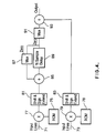
- the apparatus of Figure 2 provides two significant improvements over the prior art resizing apparatus disclosed in US-A-5355328 (Arbeiter et al). Edge conditions can be handled easily by mirroring the pixels at the image boundaries, and processing of an image in multiple segments is facilitated, as described in WO-A-9508815
- Figure 3 illustrates an octave FIR filter circuit according to an embodiment of the present invention which may be viewed as an implementation of the FIR octave filters in the resizing system of US-A-5355328 (Arbeiter et al) with advanced arithmetic to improve the precision and quality of the filters, as discussed in greater detail below.
- FIR octave filters in the resizing system of US-A-5355328 (Arbeiter et al) with advanced arithmetic to improve the precision and quality of the filters, as discussed in greater detail below.
- five filters are included.
- the filter coefficients are contained in Table 1, which is discussed in greater detail below.
- Numerical precision in a digital filter is improved by truncating or rounding the multiplier coefficients prior to multiplication and shifting the resultant multiplier product values and utilizing sign extension for restoring significance of the product values.
- the coefficients are represented as 2's complement numbers, with positive integers being represented in the usual fashion as unsigned binary integers.
- the digital filter multipliers e.g. multipliers 39, 41 and 45 in the filter illustrated in Figure 3. More particularly, leading 0's are deleted and trailing 0's are ignored for positive numbers. The leading 1's are deleted for 2's complement negative numbers and the trailing 0's are ignored. Finally, the multiplier results are shifted and sign extended in order to restore the significance of the product values being produced.
- the sum of the coefficients is 1.
- the coefficients are smaller than for filters with smaller numbers of taps, in order that the sum of the filter coefficients is 1.
- the technique is applicable except that the sum of the coefficients may differ from 1.
- Table 1 illustrates the truncated or rounded filter coefficients for 5 tap, 9 tap, 17 tap, 33 tap and 65 tap Gaussian low pass filters. As can be seen from Table 1, for wide filters the leading bits in the positive coefficients are always 0 and the leading bits in the negative coefficients are always 1. By way of contrast, the trailing bits in the coefficients for narrow filters are all 0.
- the precision of the filter coefficients may be extended for a given size multiplier.
- the trailing 0's are discarded where they exceed the precision in the 5 tap case.
- the 17 tap, 33 tap and 65 tap cases there are no trailing 0's to be discarded.
- the step of switching between a 2's complement and unsigned multiplier corresponds to shifting the significance of the generated product.
- the shift and sign extension step shown in relation to the 9 tap, 17 tap, 33 tap and 65 tap filters effectively restores the significance of the data after the multiplication has taken place.
- the 6 most significant digits can be selected. Significance of the 2's complement product is restored by right shifting the results with sign extension. This technique utilizes the significance of the product to extend the effective precision of the input data.
- the filter coefficients are the same for both vertical and horizontal directions.
- the method described in WO-A-9510883 is employed in the apparatus herein described to extend the use of the 65 tap filter for resize factors above the fifth octave. This technique has been applied both horizontally and vertically for the present apparatus.
- Input line 31 carries video signal sample values from successive input lines L1, L2... L6, L7... etc. which form the relatively long scan-line sampling periods in the vertical direction of a video image.
- L1, L2... L7 and L8 represent eight successive relatively long horizontal scan lines of the video image (with each scan line comprising a large number of pixel sample values).
- multiplier 39 receives, in turn, as a multiplicand each of all the successive input lines L1, L2... L6, L7... of sample values, and receives as a multiplier one of the truncated 6-bit filter coefficients h(-2) or h(-1) from ROM 37 (see Table 1 of the truncated kernel function coefficients.
- multiplier 41 receives, in turn, as a multiplicand each of the successive input lines L3, L4... L8, L9... of sample values, and receives as a multiplier one of the truncated 6-bit filter coefficients h(1) or h(0) from ROM 40.
- multiplier 45 receives, in turn, as a multiplicand each of the successive odd-numbered input lines L5, L7, L9... of sample values, and receives as a multiplier the truncated 6-bit filter coefficient h(2).
- each of the successive input lines L1... L9... comprises N sample values, where N may be any positive integer. However, for illustrative purposes, it is assumed that each of these successive input lines is a scan line of a video image, occupying a scan-line period, and N is the number of pixel sample values in such a scan line.
- the 14 bit output of multiplier 39 is shifted and sign extended to restore significance to the intermediate product integers output for multiplier 39 via shift and sign extend circuit 47.
- the output of shift and sign extend circuit 47 is applied as a first input to summer 53 and the output of summer 53 is applied as an input to first N-sample delay circuit 57.
- the output of the first N-sample delay circuit 57 is applied both as a first input to multiplexer 55 and as a first input to multiplexer 59.
- a zero value is applied as a second input to both multiplexers 55 and 59.
- the output of multiplexer 55 is applied as a second input to summer 53 and the output of multiplexer 59 is applied as a first input to summer 61.
- the output from multiplier 41 is shift and sign extended via circuit 49 as discussed above, and the output of the shift and sign extend circuit 49 is applied as a second input to summer 61.
- the output of summer 61 is applied as an input to a second N-sample delay circuit 65.
- the output from the second N-sample delay circuit 65 is applied as a first input to multiplexer 63, and as a first input to an additional multiplexer 66.
- a zero value is applied as a second input to each of multiplexers 63 and 66.
- the output from multiplexer 63 is applied as a third input to summer 61 and the output from multiplexer 66 is applied as a first input to summer 67.
- the output from multiplier 45 is shifted and sign extended via circuit 51, and the shifted and sign extended intermediate product signal output from circuit 51 is applied as a second input to summer 67.
- the output from summer 67 comprises the octave prefilter decimated output signal.
- each multiplier and summer includes an individual sample latch (not shown) at each of its inputs and at its outputs, with each latch introducing a one sample delay in the flow of data.
- suitable timing and control circuitry (not shown) is provided for controlling the flow of data through the octave prefilter structure of Figure 3 as discussed presently.
- the settings of multiplexers 55 and 63 are such that the respective outputs of first and second N-sample delay circuits 57 and 65 are recirculated only during even input-line scan-line period cycles of operation and zero values are normally recirculated during all odd input-line scan-line period cycles of operation.
- multiplexers 55 and 63 be in their zero value stage during those odd input-line scan-line period cycles of operation, such as during the initial cycle, where it is known a priori that no sample values can be emerging from the respective outputs of the first and second N-sample delay circuits 57 and 65.
- the setting of multiplexers 59 and 66 is such that the outputs of N-sample delay circuits 57 and 65 are translated respectively therethrough to the inputs of summers 61 and 67 only during odd input-line scan-line period cycles of operation and zero values are translated therethrough to the first inputs of summers 61 and 67 during even input-line scan-line period cycles of operation.
- each of the N samples of input line L1 is first multiplied by coefficient h(-2), to provide a sample value h(-2)s L1 and then each of these sample values is shifted and sign extended via circuit 47 to restore significance to the product signal and then applied through summer 53 as an input to the first N-sample delay means 57.
- multiplexer 55 is in its non-zero state, so that the sample values h(-2) sL1 now emerging as an output from the N-sample delay circuit 57 are recirculated back as a second input to summer 53 and are added to the corresponding h(-1) sL2 samples now being applied as a first input to summer 53 (ie ROM 37 generates the appropriate truncated 6-bit kernel-function weighting coefficient which is multiplied by the N samples of the second input line L2 in multiplier 39 and shifted and sign extended via circuit 47).
- the sample value of each sample applied as an input to the first N-sample delay circuit 57 is h(-2) sL1 + h(-1) sL2.
- multiplexer 59 is in its zero state, so that the h(-2) sL1 value output from delay circuit 57 is not applied to the first input of summer 61.
- both multiplexers 55 and 63 are in their zero state, so that no recirculation takes place of the h(-2) sL1 + h(-1) sL2 valued samples output from the first N-sample delay circuit 57 to the summer 53.
- multiplexer 59 is now in its non-zero state, so that the h(-2) sL1 + h(-1) sL2 valued samples output from delay circuit 57 are forwarded through multiplexer 59 to the first input of summer 61.
- h(-2) sL1 + h(-1) sL2 + h(0) sL3 valued samples are applied as an input to the second N-sample delay circuit 65 (i.e. ROM 40 generates the h(0) kernel function weighting coefficient in 6-bit truncated form, which is multiplied by the N-samples of input scan-line L3 via multiplier 41, the intermediate product signal output of which is shifted and sign extended via circuit 49 and applied to summer 61).
- both multiplexers 55 and 63 are in the non-zero state, so that recirculation takes place of the h(-2) sL1 + h(-1) sL2 + h(0) sL3 valued samples being output from the second N-sample delay circuit 65 back to the summer 61 as a third input thereto.
- ROM 40 generates the 6-bit truncated kernel function weighting coefficient h(1) for multiplication by the N-samples of input line L4 via multiplier 41.
- the intermediate product signal output from multiplier 41 is shifted and sign extended via circuit 49 and applied to summer 61 so that the output of summer 61 generates a summation of samples h(-2) sL1 + h(-1) sL2 + h(0) sL3 + h(1) sL4. This summation of samples is now applied to the input of N-sample delay circuit 65.
- multiplexers 59 and 66 are now in the zero state, so that while the h(-2) sL3 valued samples now emerging from the output of the first N-sample circuit 57 are recirculated back to the second input of summer 53, these h(-2) sL3 valued samples are not forwarded to the first input of summer 61, and the h(-2) sL1 + h(-1) sL2 + h(0) sL3 valued samples now emerging as an output from second N-sample delay circuit 65 are not forwarded to the first input of summer 67.
- the recirculated h(-2) sL3 valued samples are now added to the h(-1) sL4 valued samples in summer 53 and the resulting h(-2) sL3 + h(-1) sL4 valued samples are applied to the input of first N-sample delay circuit 57.
- both of multiplexers 55 and 63 are in their zero state, so that no recirculation takes place of the h(-2) sL3 + h(-1) sL4 valued samples now emerging as an output from first N-sample delay circuit 57 back as a second input to summer 53.
- multiplexers 59 and 66 are in the non-zero state, so that the h(-2) sL3 + h(-1) sL4 valued samples are forwarded through multiplexer 59 to the first input of summer 61 and the h(-2) sL1 + h(-1) sL2 + h(0) sL3 + h(1) sL4 valued samples now emerging from the second N-sample delay circuit 65 are applied to the first input of summer 67.
- ROM 43 generates 6-bit truncated kernel-function weighting coefficient h(2) which is multiplied by the N-samples of scan-line L5 and multiplier 45, the intermediate product signal output of which is shifted and sign extended via circuit 51 and applied as a second input to summer 67, thereby deriving a first filtered output line comprising h(-2) sL1 + h(-1) sL2 + h(0) sL3 + h(1) sL4 + h(2) sL5 valued samples, from the first 5-tap octave prefilter structure of Figure 3.
- the status of the h(-2) sL3 + h(-1) sL4 valued samples during the fifth scan-line period cycle of operation is identical to the status of the h(-2) sL1 + h(-1) sL2 valued samples during the third scan-line period cycle of operation.
- the sixth and seventh scan-line period cycles of operation will correspond, respectively, to the fourth and fifth scan-line period cycles of operation.
- the second filtered output line comprising h(-2) sL3 + h(-1) sL4 + h(0) sL5 + h(1) sL6 + h(2) sL7 valued samples, will be derived in the seventh scan-line period cycle of operation.
- the third filtered output line comprising h(-2) sL5 + h(-1) sL6 + h(0) sL7 + h(1) sL8 + h(2) sL9 valued samples, will be derived in the ninth scan-line period cycle of operation while the fourth filtered output line, comprising h(-2) sL7 + h(-1) sL8 + h(0) sL9 + h(1) sL10 + h(2) sL11 valued samples, will be derived in the eleventh scan-line period cycle of operation, and so forth.
- the structure of Figure 3 may be used to implement a 9 tap, 17 tap, 33 tap, 65 tap, etc. structure by applying the appropriate truncated kernel-function weighting coefficients from ROMs 37, 40 and 43 to multipliers 39, 41 and 45 in accordance with the appropriate timing control.
- the truncated intermediate product signals output from multipliers 39, 41 and 45 are shifted and sign extended via circuits 47, 49 and 51 in the manner discussed above.
- ROM 37 operates cyclically to forward each of the four kernel-function weighting coefficients h(-4), h(-3), h(-2) and h(-1) from Table 1, in turn, to the multiplier input of multiplier 39.
- ROM 40 also operates cyclically to forward each of the four kernel-function weighting coefficients h(0), h(1), h(2), and h(3) from Table 1, in turn, to the multiplier input of multiplier 41.
- ROM 43 generates the truncated kernel-function weighting coefficient h(4) and directly applies it to the input of multiplier 45.
- timing control of multiplexers 59 and 66 is such that they are in the non-zero state only during scan-line period cycles of operation 1, 5, 9, 13... and are in the zero state during other scan-line period cycles of operation.
- the h(-4) sL1 valued samples are applied to the input of the first N-sample delay circuit 57 during the first scan-line period cycle of operation.
- successive older recirculated sample values emerging as an output from the first N-sample delay circuit 57, that are applied to the second input of summer 53 are added to new sample values that are applied to the first input of summer 53 (in the manner described above in connection with the 5-tap decimating filter implementation of Figure 3).
- these h(-4) sL1 + h(-3) sL2 + h(-2) sL3 + h(-1) sL4 valued samples are forwarded to the first input of summer 61, where they are added to h(0) sL5 valued samples applied to the second input of summer 61 before being applied as an input to second N-sample delay circuit 65.
- the value of samples constituting the second filtered output line is h(-4) sL5 + h(-3) sL6 + h(-2) sL7 + h(-1) sL8 + h(0) sL9 + h(1) sL10 + h(2) sL11 + h(3) sL12 + h(4) sL13; and so forth.
- the resizing apparatus described in US-A-5355328 requires that different filters be applied for each octave for image reduction or magnification. When these filters are changed at the boundaries of the reduction or magnification, there is potentially an undesirable visible difference between the image that is filtered with one octave prefilter and the image that is filtered by the next octave prefilter.
- the circuit of the present embodiment includes the use of 5 octave filters that all have the same archetype. This is sometimes referred to as the "Q" of a filter or the damping factor ("Filter Theory and Design: Active and Passive" by Adel S. Sedra and Peter 0. Bracket, Matrix Publishers 1978).
- the octave filters implemented in Figure 3 can be designed by first designing the half band filter and over-sampling the impulse response of the half band filter to achieve the higher reduction filters.
- the impulse response of the filter, h(t) may be calculated using any of a number of commercially available software packages.
- the FIR filter taps of the filter are equal to the corresponding values of the impulse response of the filter, (i.e.
- the filter coefficients are 0.65, 0.525, 0.25, 0.025, -0.0625.
- the filter coefficients need to be normalized so that the gain of the filter is equal to 1.
- the normalised coefficients are .304688, .246094, .117188, .011719, -.023744. These are the filter coefficients given in Table 1 in binary form. The conversion to integer binary form requires a well known adjustment for integer arithmetic.
- the filter means of the alternative embodiment shown in Figure 4 is unique in that it is a 3 tap filter. It is believed that a person skilled in the art would not expect that a 3 tap filter could be used in a high quality video processing architecture. However, the use of a 3 tap half band filter on the upsampled signal that is produced by the interpolation means produces a much higher quality output than would normally be expected.
- the filter coefficients that are contained in Table 2 describe the filters that are used with this second filter means.
- the first octave is filtered using a 3 tap finite impulse response (FIR) filter and the second octave is filtered using a 5 tap FIR filter and the third octave is filtered using a 9 tap FIR filter and the fourth octave is filtered using a 17 tap FIR filter and the fifth octave is filtered using a 33 tap FIR filter and all higher octaves are filtered using a 33 tap FIR filter, as described in WO-A-9508867.
- FIR finite impulse response
- the filter coefficients are all positive.
- the input to the multipliers that selects between 2's complement and normal operation is unused.
- the multipliers are still required to operate on 2's complement data and unsigned filter coefficients.
- the filter coefficients are still shifted and sign extended as in the case in which both signed and unsigned filter coefficients are used.
- the filter coefficients are the same for both vertical and horizontal directions.
- the method described in WO-A-9510883 has been employed to extend the use of the 33 tap filter for resize factors above the fifth octave. This technique has been applied both horizontally and vertically. A more detailed discussion of the circuit of Figure 4 will now be presented.
- Input line 71 carries video signal sample values from successive input lines L1, L2... L6, L7... etc. which form the relatively long scan-line sampling periods in the vertical direction of a video image.
- L1, L2... L7 and L8 represent eight successive relatively long horizontal scan lines of the video image (with each scan line comprising a large number of pixel sample values).
- multiplier 77 receives, in turn, as a multiplicand each of all the successive input lines L1, L2... L6, L7... of sample values, and receives as a multiplier one of the truncated 4-bit filter coefficients h(-1) or h(0) from ROM 75 (see Table 2 of the truncated kernel function coefficients).
- multiplier 79 receives, in turn, as a multiplicand each of the successive odd input lines L3, L5, L7, L9... of sample values, and receives as a multiplier the truncated 4-bit filter coefficient h(1) from ROM 78.
- each of the successive input lines L1... L9... comprises N sample values, where N may be any positive integer.
- N may be any positive integer.
- it is assumed that each of these successive input lines is a scan line of a video image, occupying a scan-line period, and N is the number of pixel sample values in such a scan line.
- multiplier 77 As discussed above with reference to Table 2, the 12 bit output of multiplier 77 is shifted and sign extended to restore significance to the intermediate product integers output for multiplier 77 via shift and sign extend circuit 81.
- the output of shift and sign extend circuit 81 is applied as a first input to summer 85 and the output of summer 85 is applied as an input to N-sample delay circuit 89.
- the output of the N-sample delay circuit 89 is applied both as a first input to multiplexer 87 and as a first input to multiplexer 91.
- a zero value is applied as a second input to both multiplexers 87 and 91.
- the output of multiplexer 87 is applied as a second input to summer 85 and the output of multiplexer 91 is applied as a first input to summer 93.
- the output from multiplier 79 is shift and sign extended via circuit 83 as discussed above, and the output of the shift and sign extend circuit 83 is applied as a second input to summer 93.
- the output from summer 93 comprises the octave prefilter decimated output signal.
- each multiplier and summer includes an individual sample latch (not shown) at each of its inputs and at its outputs, with each latch introducing a one sample delay in the flow of data.
- timing and control circuitry (not shown) is provided for controlling the flow of data through the octave prefilter structure of Figure 4.
- the setting of multiplexer 87 is such that the output of N-sample delay circuit 89 is recirculated only during even input-line scan-line period cycles of operation and zero values are normally recirculated during all odd input-line scan-line period cycles of operation. (Although in principle, it is not absolutely essential that multiplexer 87 be in its zero value stage during those odd input-line scan-line period cycles of operation, such as during the initial cycle, where it is known a priori that no sample values can be emerging from the output of N-sample delay circuit 89).
- the setting of multiplexer 91 is such that the output of N-sample delay circuit 89 is translated therethrough to the input of summer 93 only during odd input-line scan-line period cycles of operation and zero values are translated therethrough to the first input of summer 93 during even input-line scan-line period cycles of operation.
- each of the N samples of input line L1 is first multiplied by coefficient h(-1), to provide a sample value h(-1)s L1 and then each of these sample values is shifted and sign extended via circuit 81 to restore significance to the product signal and then applied through summer 85 as an input to the N-sample delay means 89.
- multiplexer 87 is in its non-zero state, so that the sample values h(-1) sL1 now emerging as an output from the N-sample delay circuit 89 are recirculated back as a second input to summer 85 and are added to the corresponding h(0) sL2 samples now being applied as a first input to summer 85 (ie ROM 75 generates the appropriate truncated 4-bit kernel-function weighting coefficient which is multiplied by the N samples of the second input line L2 in multiplier 77 and shifted and sign extended via circuit 81).
- the sample value of each sample applied as an input to the N-sample delay circuit 89 is h(-1) sL1 + h(0) sL2.
- multiplexer 91 is in its zero state, so that the h(-1) sL1 value output from delay circuit 89 is not applied to the first input of summer 93.
- multiplexer 87 is in its zero state, so that no recirculation takes place of the h(-1) sL1 + h(0) sL2 valued samples output from the N-sample delay circuit 89 to the summer 85.
- multiplexer 91 is now in its non-zero state, so that the h(-1) sL1 + h(0) sL2 valued samples output from delay circuit 89 are forwarded through multiplexer 91 to the first input of summer 93.
- h(-1) sL1 + h(0) sL2 + h(1) sL3 valued samples are output from the filter (ie. ROM 78 generates the appropriate truncated 4-bit kernel-function weighting coefficient which is multiplied by the N samples of the third input line L3 in multiplier 79 and shifted and sign extended via circuit 83).
- ROM 75 During the fourth scan-line period cycle of operation, ROM 75 generates the 4-bit truncated kernel function weighting coefficient h(0) for multiplication by the N-samples of input line L4 via multiplier 77.
- the intermediate product signal output from multiplier 77 is shifted and sign extended via circuit 81 and applied to summer 85 so that the output of summer 85 is input to N-sample delay 89 since the multiplexer 87 is in its non-zero state.
- multiplexer 87 is in its zero state, so that no recirculation takes place of the h(-1) sL3 + h(0) sL4 valued samples now emerging as an output from N-sample delay circuit 89 back as a second input to summer 85.
- multiplexer 91 is in the non-zero state, so that the h(-1) sL3 + h(0) sL4 valued samples are forwarded through multiplexer 91 to the first input of summer 93.
- the ROM 78 generates the 4-bit truncated kernel function weighting coefficient h(1) for multiplications by the N-samples of input line L5 via multiplier 79.
- the intermediate product signal output from multiplier 79 is shifted and sign extended via circuit 83 and applied to summer 93.
- h(-1) sL3 + h(0) sL4 + h(1) sL5 valued samples are output from the filter.
- the status of the h(-1) sL3 + h(0) sL4 valued samples during the fifth scan-line period cycle of operation is identical to the status of the h(-1) sL1 + h(0) sL2 valued samples during the third scan-line period cycle of operation.
- the sixth and seventh scan-line period cycles of operation will correspond, respectively, to the fourth and fifth scan-line period cycles of operation.
- the second filtered output line comprising h(-1) sL3 + h(0) sL4 + h(1) sL5 valued samples, will be derived in the fifth scan-line period cycle of operation.
- the third filtered output line comprising h(-1) sL5 + h(0) sL6 + h(1) sL7 valued samples, will be derived in the seventh scan-line period cycle of operation while the fourth filtered output line, comprising h(-1) sL7 + h(0) sL8 + h(1) sL9 valued samples, will be derived in the ninth scan-line period cycle of operation, and so forth.
- the structure of Figure 4 may be used to implement a 5 tap, 9 tap, 17 tap, and 33 tap structure by applying the appropriate truncated kernel-function weighting coefficients from ROMs 75 and 78 to multipliers 77 and 79 in accordance with the appropriate timing control.
- the truncated intermediate product signals output from multipliers 77 and 79 are shifted and sign extended via circuits 81 and 83 in the manner discussed above.
Landscapes
- Physics & Mathematics (AREA)
- General Physics & Mathematics (AREA)
- Engineering & Computer Science (AREA)
- Theoretical Computer Science (AREA)
- Image Processing (AREA)
- Editing Of Facsimile Originals (AREA)
- Complex Calculations (AREA)
- Studio Circuits (AREA)
- Controls And Circuits For Display Device (AREA)
- Holo Graphy (AREA)
- Apparatus For Radiation Diagnosis (AREA)
Claims (15)
- Einrichtung zum Ändern der Größe eines Bilds, umfassend:a) eine Interpolierfiltervorrichtung, die einen Eingabepixelstrom empfängt, der eine vorbestimmte Abtastperiode P und eine erste Abtastrate von S Pixeln/Zeile hat, und den Strom der Eingabepixel mit einer vorbestimmten Interpolierrate interpoliert und einen ersten abgeleiteten Pixelabtaststrom erzeugt, der eine weitere Abtastperiode (M/(CL))P und eine zweite Abtastrate von T Pixeln/Zeile aufweist, wobei L eine erste positive Ganzzahl größer als eins ist, C eine positive Ganzzahl und M kleiner als CL ist, und wobei entweder 2nM/CL oder 2-nM/CL gleich dem Zeitschritt-Inkrement M/L und der Betrag von n wenigstens gleich null ist;b) eine Oktavfiltervorrichtung, die eine vorbestimmte Abtastrate hat, die mit der Interpolierrate des Interpolierfilters verknüpft ist, und den ersten abgeleiteten Pixelabtaststrom empfängt und daraus einen gefilterten Ausgabepixelstrom erzeugt, der eine Abtastrate von (M/L)P aufweist, wobei die Oktavfiltervorrichtung eine Anzahl Filterkoeffizienten hat, und die positiven Koeffizienten durch vorzeichenlose binäre Ganzzahlen dargestellt werden und die negativen Koeffizienten durch binäre Zweierkomplement-Ganzzahlen dargestellt werden, und die Oktavfiltervorrichtung umfaßt:i) einen Eingang (31, 33, 35; 71, 73), der einen ersten abgeleiteten Pixelabtaststrom empfängt, von denen jedes Pixel eine vorbestimmte Bitanzahl umfaßt;ii) Vorrichtungen (37, 40, 43; 75, 78) zum Abschneiden oder Runden von zumindest einer führenden "0" oder einer an letzter Stelle stehenden "0" der positiven Koeffizienten und von zumindest einer führenden "1" oder einer an letzter Stelle stehenden "0" der negativen Koeffizienten, so daß Stellen der Ganzzahlen entfernt werden;iii) Vorrichtungen (57, 65; 89), die nacheinander den ersten abgeleiteten Pixelabtaststrom verzögern und nacheinander verzögerte Versionen des ersten abgeleiteten Pixelabtaststroms erzeugen;iv) Vorrichtungen (39, 41, 45; 77, 79), die den ersten abgeleiteten Pixelabtaststrom mit entprechenden abgeschnittenen Darstellungen entsprechender Koeffizienten aus der Anzahl Filterkoeffizienten multiplizieren und daraus eine Anzahl Zwischenprodukt-Ganzzahlen erzeugen;v) Vorrichtungen (47, 49, 51; 81, 83) zum Wiederherstellen der Stellenanzahl der Zwischenprodukt-Ganzzahlen; undvi) Vorrichtungen (53, 61, 67; 85, 93), die die Zwischenprodukt-Ganzzahlen summieren und daraus den Strom gefilterter Ausgabepixel erzeugen.
- Einrichtung nach Anspruch 1, wobei die Multipliziervorrichtung (39, 41, 45; 77, 79) zudem eine Anzahl digitaler Multiplizierer umfaßt.
- Einrichtung nach Anspruch 1 oder 2, wobei die Vorrichtung (47, 49, 51; 81, 83) zum Wiederherstellen der Stellenanzahl eine Vorrichtung zum Vorzeichen-Erweitern und Schieben der Zwischenprodukt-Ganzzahlen nach rechts umfaßt.
- Einrichtung nach Anspruch 1, 2 oder 3, wobei die Vorrichtung (37, 40, 43; 75, 78) zum Abschneiden oder Runden einen digitalen Speicher zum Speichern der Koeffizienten enthält, die in abgeschnittener Form codiert sind.
- Einrichtung nach Anspruch 4, wobei der digitale Speicher drei abgeschnittene 6-Bit-Koeffizienten zum Implementieren eines Unterabtast-Halbbandfilters mit fünf Abzweigungen wie folgt speichert: h(0) = 101000; h(1), h(-1) = 010000 und h(2), h(-2) = 111100, und wobei die Vorrichtung zum Wiederherstellen der Stellenanzahl eine Vorrichtung zum Vorzeichen-Erweitern und Schieben der Zwischenprodukt-Ganzzahlen um 1 Bit nach rechts umfaßt.
- Einrichtung nach Anspruch 4, wobei der digitale Speicher einen ersten abgeschnittenen 6-Bit-Filterkoeffizienten und weitere abgeschnittene 6-Bit-Filterkoeffizienten zum Implementieren eines Unterabtast-Viertelbandfilters mit neun Abzweigungen speichert, wobei der erste abgeschnittene Filterkoeffizient h(0) = 100111 enthält, und die weiteren abgeschnittenen Filterkoeffizienten umfassen: h(1), h(-1) = 111111; h(2), h(-2) = 011110; h(3), h(-3) = 000011 und h(4), h(-4) = 111001, und wobei die Vorrichtung zum Wiederherstellen der Stellenanzahl bei den Zwischenprodukt-Ganzzahlen bezüglich einer ersten Zwischenprodukt-Ganzzahl eine Vorrichtung zum Vorzeichen-Erweitern und Schieben der ersten Zwischenprodukt-Ganzzahl um 2 Bit nach rechts umfaßt, und wobei die Vorrichtung zum Wiederherstellen der Stellenanzahl bei den zusätzlichen Zwischenprodukt-Ganzzahlen eine Vorrichtung zum Vorzeichen-Erweitern und Schieben der zusätzlichen Zwischenprodukt-Ganzzahlen um drei Bit nach rechts umfaßt.
- Einrichtung nach Anspruch 4, wobei die Vorrichtung zum Wiederherstellen der Stellenanzahl eine Vorrichtung zum Vorzeichen-Erweitern und Schieben der Zwischenprodukt-Ganzzahlen um drei Bit nach rechts umfaßt, und wobei die Koeffizienten in abgeschnittener Form in dem digitalen Speicher codiert sind, um ein Unterabtast-Achtelbandfilter mit 17 Abzweigungen wie folgt zu erzeugen:
h(0) = 100110 h(1), h(-1) = 100101 h(2), h(-2) = 011111 h(3), h(-3) = 010111 h(4), h(-4) = 001111 h(5), h(-5) = 000111 h(6), h(-6) = 000001 h(7), h(-7) = 111110 h(8), h(-8) = 111101 - Einrichtung nach Anspruch 4, wobei die Vorrichtung zum Wiederherstellen der Stellenanzahl eine Vorrichtung zum Vorzeichen-Erweitern und Schieben der Zwischenprodukt-Ganzzahlen um drei Bit nach rechts umfaßt, und wobei die Koeffizienten in abgeschnittener Form in dem digitalen Speicher codiert sind, um ein Unterabtast-Sechzehntelbandfilter mit 33 Abzweigungen wie folgt zu erzeugen:
h(0) = 010010 h(1), h(-1) = 011000 h(2), h(-2) = 010001 h(3), h(-3) = 010000 h(4), h(-4) = 001111 h(5), h(-5) = 001101 h(6), h(-6) = 001011 h(7), h(-7) = 001001 h(8), h(-8) = 000111 h(9), h(-9) = 000101 h(10), h(-10) = 000011 h(11), h(-11) = 000010 h(12), h(-12) = 000000 h(13), h(-13) = 000000 h(14), h(-14) = 111111 h(15), h(-15) = 111111 h(16), h(-16) = 111111 - Einrichtung nach Anspruch 4, wobei die Vorrichtung zum Wiederherstellen der Stellenanzahl eine Vorrichtung zum Vorzeichen-Erweitern und Schieben der Zwischenprodukt-Ganzzahlen um drei Bit nach rechts umfaßt, und wobei die Koeffizienten in abgeschnittener Form in dem digitalen Speicher codiert sind, um ein Unterabtast-Zweiunddreissigstelbandfilter mit 65 Abzweigungen wie folgt zu erzeugen:
h(0) = 001010 h(1), h(-1) = 010000 h(2), h(-2) = 001001 h(3), h(-3) = 001001 h(4), h(-4) = 001000 h(5), h(-5) = 001000 h(6), h(-6) = 001000 h(7), h(-7) = 001000 h(8), h(-8) = 000111 h(9), h(-9) = 000111 h(10), h(-10) = 000110 h(11), h(-11) = 000110 h(12), h(-12) = 000101 h(13), h(-13) = 000101 h(14), h(-14) = 000100 h(15), h(-15) = 000100 h(16), h(-16) = 000011 h(17), h(-17) = 000011 h(18), h(-18) = 000010 h(19), h(-19) = 000010 h(20), h(-20) = 000001 h(21), h(-21) = 000001 h(22), h(-22) = 000001 h(23), h(-23) = 000000 h(24), h(-24) = 000000 h(25), h(-25) = 000000 h(26), h(-26) = 000000 h(27), h(-27) = 000000 h(28), h(-28) = 000000 h(29), h(-29) = 000000 h(30), h(-30) = 000000 h(31), h(-31) = 000000 h(32), h(-12) = 000000 - Einrichtung nach Anspruch 4, wobei der digitale Speicher zwei abgeschnittene 4-Bit-Koeffizienten zum Implementieren eines Unterabtast-Halbbandfilters mit 3 Abzweigungen wie folgt speichert: h(0) = 1000; h(1), h(-1) = 0100, und wobei die Vorrichtung zum Wiederherstellen der Stellenanzahl eine Vorrichtung zum Vorzeichen-Erweitern und Schieben der Zwischenprodukt-Ganzzahlen um 1 Bit nach rechts umfaßt.
- Einrichtung nach Anspruch 4, wobei der digitale Speicher einen ersten abgeschnittenen 4-Bit-Filterkoeffizienten und weitere abgeschnittene 4-Bit-Filterkoeffizienten zum Implementieren eines Unterabtast-Viertelbandfilters mit fünf Abzweigungen speichert, wobei der erste abgeschnittene Filterkoeffizient h(0) = 1001 enthält, und die weiteren abgeschnittenen Filterkoeffizienten umfassen: h(1), h(-1) = 1110 und h(2), h(-2) = 0111, und wobei die Vorrichtung zum Wiederherstellen der Stellenanzahl bei den Zwischenprodukt-Ganzzahlen bezüglich einer ersten Zwischenprodukt-Ganzzahl eine Vorrichtung zum Vorzeichen-Erweitern und Schieben der ersten Zwischenprodukt-Ganzzahl um 2 Bit nach rechts umfaßt, und wobei die Vorrichtung zum Wiederherstellen der Stellenanzahl bei den zusätzlichen Zwischenprodukt-Ganzzahlen eine Vorrichtung zum Vorzeichen-Erweitern und Schieben der zusätzlichen Zwischenprodukt-Ganzzahlen um drei Bit nach rechts umfaßt.
- Einrichtung nach Anspruch 4, wobei die Vorrichtung zum Wiederherstellen der Stellenanzahl eine Vorrichtung zum Vorzeichen-Erweitern und Schieben der Zwischenprodukt-Ganzzahlen um drei Bit nach rechts umfaßt, und wobei die Koeffizienten in abgeschnittener Form in dem digitalen Speicher codiert sind, um ein Unterabtast-Achtelbandfilter mit 9 Abzweigungen wie folgt zu erzeugen:
h(0) = 1010 h(1), h(-1) = 1001 h(2), h(-2) = 0100 h(3), h(-3) = 0110 h(4), h(-4) = 0100 - Einrichtung nach Anspruch 4, wobei die Vorrichtung zum Wiederherstellen der Stellenanzahl eine Vorrichtung zum Vorzeichen-Erweitern und Schieben der Zwischenprodukt-Ganzzahlen um drei Bit nach rechts umfaßt, und wobei die Koeffizienten in abgeschnittener Form in dem digitalen Speicher codiert sind, um ein Unterabtast-Sechzehntelbandfilter mit 17 Abzweigungen wie folgt zu erzeugen:
h(0) = 0110 h(1), h(-1) = 0101 h(2), h(-2) = 0100 h(3), h(-3) = 0100 h(4), h(-4) = 0100 h(5), h(-5) = 0100 h(6), h(-6) = 0011 h(7), h(-7) = 0011 h(8), h(-8) = 0010 - Einrichtung nach Anspruch 4, wobei die Vorrichtung zum Wiederherstellen der Stellenanzahl eine Vorrichtung zum Vorzeichen-Erweitern und Schieben der Zwischenprodukt-Ganzzahlen um drei Bit nach rechts umfaßt, und wobei die Koeffizienten in abgeschnittener Form in dem digitalen Speicher codiert sind, um ein Unterabtast-Sechzehntelbandfilter mit 33 Abzweigungen wie folgt zu erzeugen:
h(0) = 0100 h(1), h(-1) = 0011 h(2), h(-2) = 0011 h(3), h(-3) = 0010 h(4), h(-4) = 0010 h(5), h(-5) = 0010 h(6), h(-6) = 0010 h(7), h(-7) = 0010 h(8), h(-8) = 0010 h(9), h(-9) = 0010 h(10), h(-10) = 0010 h(11), h(-11) = 0010 h(12), h(-12) = 0010 h(13), h(-13) = 0010 h(14), h(-14) = 0001 h(15), h(-15) = 0001 h(16), h(-16) = 0001. - Verfahren zum Gebrauch einer Einrichtung gemäß irgendeinem der vorhergehenden Ansprüche, geeignet zum Ändern der Größe eines Bilds, wobei in dem Verfahren die Interpolierfiltervorrichtung zum Ausrichten des Eingangspixelstroms und des ersten abgeleiteten Abtastpixelstroms an den Bildgrenzen verwendet wird.
Applications Claiming Priority (3)
| Application Number | Priority Date | Filing Date | Title |
|---|---|---|---|
| US125530 | 1993-09-22 | ||
| US08/125,530 US5559905A (en) | 1993-09-22 | 1993-09-22 | Digital image resizing apparatus |
| PCT/CA1994/000532 WO1995008814A1 (en) | 1993-09-22 | 1994-09-21 | Digital image resizing apparatus |
Publications (2)
| Publication Number | Publication Date |
|---|---|
| EP0723688A1 EP0723688A1 (de) | 1996-07-31 |
| EP0723688B1 true EP0723688B1 (de) | 1999-06-16 |
Family
ID=22420140
Family Applications (1)
| Application Number | Title | Priority Date | Filing Date |
|---|---|---|---|
| EP94928235A Expired - Lifetime EP0723688B1 (de) | 1993-09-22 | 1994-09-21 | Digitale vorrichtung zur änderung der grösse eines bildes und verwendungsmethode desgleichen |
Country Status (8)
| Country | Link |
|---|---|
| US (1) | US5559905A (de) |
| EP (1) | EP0723688B1 (de) |
| JP (1) | JPH09507314A (de) |
| KR (1) | KR100301543B1 (de) |
| AT (1) | ATE181435T1 (de) |
| AU (1) | AU7736994A (de) |
| DE (1) | DE69419167T2 (de) |
| WO (1) | WO1995008814A1 (de) |
Families Citing this family (16)
| Publication number | Priority date | Publication date | Assignee | Title |
|---|---|---|---|---|
| US5835160A (en) * | 1995-09-13 | 1998-11-10 | Oak Technology, Inc. | Sampling rate conversion using digital differential analyzers |
| JP4191246B2 (ja) * | 1995-11-08 | 2008-12-03 | ジェネシス マイクロチップ インク | 映像フィールドを順次走査映像フレームへ非飛び越し走査するための方法および装置 |
| US6101293A (en) * | 1997-10-20 | 2000-08-08 | Moore U.S.A., Inc. | Digital special pantograph |
| US6239842B1 (en) | 1998-12-18 | 2001-05-29 | Oplus Technologies Ltd. | Method of de-interlacing video signals using a mixed mode spatial and temporal approximation technique |
| JP2000251090A (ja) * | 1999-03-01 | 2000-09-14 | Sony Computer Entertainment Inc | 描画装置及び該描画装置で被写界深度を表現する方法 |
| US7890566B1 (en) * | 2000-02-18 | 2011-02-15 | Texas Instruments Incorporated | Microprocessor with rounding dot product instruction |
| US6950115B2 (en) * | 2001-05-09 | 2005-09-27 | Clairvoyante, Inc. | Color flat panel display sub-pixel arrangements and layouts |
| US20040162865A1 (en) * | 2001-05-17 | 2004-08-19 | Kornelis Meinds | Method and apparatus for executing an affine or non-affine transformation |
| US7142729B2 (en) * | 2001-09-10 | 2006-11-28 | Jaldi Semiconductor Corp. | System and method of scaling images using adaptive nearest neighbor |
| US6993207B1 (en) | 2001-10-05 | 2006-01-31 | Micron Technology, Inc. | Method and apparatus for electronic image processing |
| US20070165192A1 (en) * | 2006-01-13 | 2007-07-19 | Silicon Optix Inc. | Reduced field angle projection display system |
| US7714943B2 (en) * | 2002-06-12 | 2010-05-11 | Geo Semiconductor Inc. | Ultra-thin image projection system |
| US7145936B2 (en) * | 2002-12-23 | 2006-12-05 | International Business Machines Corporation | Bandpass delta sigma truncator and method of truncating a multi-bit digital signal |
| TWI231886B (en) * | 2003-01-08 | 2005-05-01 | Silicon Optix Inc | Image projection system and method |
| US20080285888A1 (en) * | 2007-05-15 | 2008-11-20 | Yang-Hung Shih | Image resizing device and parameter adjusting method thereof |
| CN112886944B (zh) * | 2019-11-29 | 2024-09-10 | 西安诺瓦星云科技股份有限公司 | 滤波器系数生成方法及装置 |
Family Cites Families (15)
| Publication number | Priority date | Publication date | Assignee | Title |
|---|---|---|---|---|
| US4551753A (en) * | 1981-12-17 | 1985-11-05 | Nippon Hoso Kyokai | Picture signal processing system including spatio-temporal filter |
| JPS5951686A (ja) * | 1982-09-02 | 1984-03-26 | Hitachi Medical Corp | デイジタルフイルタ法及びデイジタルフイルタ |
| US4674125A (en) * | 1983-06-27 | 1987-06-16 | Rca Corporation | Real-time hierarchal pyramid signal processing apparatus |
| NL8501834A (nl) * | 1985-06-26 | 1987-01-16 | Philips Nv | Egalisatie-inrichting met verschuifbare bandfilters en een digitaal filter eventueel te gebruiken in de egalisatie-inrichting. |
| GB2181318B (en) * | 1985-10-04 | 1989-12-28 | Sony Corp | Two-dimensional finite impulse response filters |
| US4779217A (en) * | 1985-12-27 | 1988-10-18 | Kyocera Corporation | Octave multiple filter |
| US4797942A (en) * | 1987-03-02 | 1989-01-10 | General Electric | Pyramid processor for building large-area, high-resolution image by parts |
| EP0397807A4 (en) * | 1988-07-13 | 1992-08-12 | Analogic Corporation | Apparatus for simultaneously filtering and resampling digital data |
| DE69028075T2 (de) * | 1989-06-16 | 1997-03-13 | Eastman Kodak Co | Digitaler bildinterpolator |
| GB9012423D0 (en) * | 1990-06-04 | 1990-07-25 | Abekas Video Systems | Video image transformation |
| JP2991485B2 (ja) * | 1990-11-29 | 1999-12-20 | 株式会社東芝 | 画像処理装置 |
| JP2906791B2 (ja) * | 1990-12-21 | 1999-06-21 | ミノルタ株式会社 | 画像処理装置 |
| WO1992012495A1 (en) * | 1990-12-31 | 1992-07-23 | E.I. Du Pont De Nemours And Company | Method of resizing an image, designing a filter therefor, and mapping the output image to the input image |
| US5355328A (en) * | 1991-09-27 | 1994-10-11 | Northshore Laboratories, Inc. | Resampling apparatus suitable for resizing a video image |
| WO1994024632A1 (en) * | 1993-04-14 | 1994-10-27 | Northshore Laboratories, Inc. | Resampling apparatus suitable for resizing a video image |
-
1993
- 1993-09-22 US US08/125,530 patent/US5559905A/en not_active Expired - Lifetime
-
1994
- 1994-09-21 EP EP94928235A patent/EP0723688B1/de not_active Expired - Lifetime
- 1994-09-21 AT AT94928235T patent/ATE181435T1/de not_active IP Right Cessation
- 1994-09-21 DE DE69419167T patent/DE69419167T2/de not_active Expired - Lifetime
- 1994-09-21 AU AU77369/94A patent/AU7736994A/en not_active Abandoned
- 1994-09-21 KR KR1019960701509A patent/KR100301543B1/ko not_active Expired - Fee Related
- 1994-09-21 WO PCT/CA1994/000532 patent/WO1995008814A1/en not_active Ceased
- 1994-09-21 JP JP7509469A patent/JPH09507314A/ja active Pending
Also Published As
| Publication number | Publication date |
|---|---|
| EP0723688A1 (de) | 1996-07-31 |
| US5559905A (en) | 1996-09-24 |
| WO1995008814A1 (en) | 1995-03-30 |
| JPH09507314A (ja) | 1997-07-22 |
| AU7736994A (en) | 1995-04-10 |
| DE69419167T2 (de) | 1999-10-14 |
| DE69419167D1 (de) | 1999-07-22 |
| ATE181435T1 (de) | 1999-07-15 |
| KR100301543B1 (ko) | 2001-10-22 |
Similar Documents
| Publication | Publication Date | Title |
|---|---|---|
| US5559905A (en) | Digital image resizing apparatus | |
| US4328426A (en) | Filter for image pixels | |
| US5374995A (en) | Method and apparatus for enhancing sharpness of a sequence of images subject to continuous zoom | |
| US5355328A (en) | Resampling apparatus suitable for resizing a video image | |
| US5410616A (en) | Loop-up table image scaling for rational factors | |
| US5202670A (en) | Image processing apparatus | |
| US5801678A (en) | Fast bi-linear interpolation pipeline | |
| EP0853292A2 (de) | Interpolator und Verfahren zur Interpolierung von digitalen Signalmustern | |
| EP0523924B1 (de) | Bildsignalverarbeitungsgerät | |
| US4328425A (en) | Filter for image pixels | |
| JPH05308250A (ja) | サンプル・データ補間装置 | |
| US20100215284A1 (en) | System and Method for Implementing Graphics and Video Scaling Algorithm Using Interpolation Based on Symmetrical Polyphase Filtering | |
| EP0721632B1 (de) | Spiegelbild- und erweiterungsfunktion für digitale filterung | |
| US5479454A (en) | Digital filter with improved numerical precision | |
| US7149364B2 (en) | Mean filter device and filtering method | |
| Wang et al. | Efficient implementation of a cubic-convolution based image scaling engine | |
| EP0694188B1 (de) | Wiederbemusterungsvorrichtung insbesondere zur aenderung der groesse von videobildern | |
| JPH11203467A (ja) | 表示装置および表示方法 | |
| CA2102936C (en) | Combined aligner blender | |
| JPH07121705A (ja) | 画像処理方法及び装置 | |
| Ramachandran et al. | Design and FPGA implementation of a video scalar with on-chip reduced memory utilization | |
| JP3661156B2 (ja) | ビデオ画像のサイズを再調整するのに好適な再サンプリング装置 | |
| JP3025437B2 (ja) | 元のデジタル画像を処理する方法及び装置 | |
| GB2304014A (en) | Method and apparatus for uniformly scaling a digital image | |
| Raghupathy et al. | VLSI architecture and design for high performance adaptive video scaling |
Legal Events
| Date | Code | Title | Description |
|---|---|---|---|
| PUAI | Public reference made under article 153(3) epc to a published international application that has entered the european phase |
Free format text: ORIGINAL CODE: 0009012 |
|
| 17P | Request for examination filed |
Effective date: 19960416 |
|
| AK | Designated contracting states |
Kind code of ref document: A1 Designated state(s): AT BE CH DE DK ES FR GB GR IE IT LI LU MC NL PT SE |
|
| 17Q | First examination report despatched |
Effective date: 19970612 |
|
| GRAG | Despatch of communication of intention to grant |
Free format text: ORIGINAL CODE: EPIDOS AGRA |
|
| GRAG | Despatch of communication of intention to grant |
Free format text: ORIGINAL CODE: EPIDOS AGRA |
|
| GRAH | Despatch of communication of intention to grant a patent |
Free format text: ORIGINAL CODE: EPIDOS IGRA |
|
| GRAH | Despatch of communication of intention to grant a patent |
Free format text: ORIGINAL CODE: EPIDOS IGRA |
|
| GRAA | (expected) grant |
Free format text: ORIGINAL CODE: 0009210 |
|
| AK | Designated contracting states |
Kind code of ref document: B1 Designated state(s): AT BE CH DE DK ES FR GB GR IE IT LI LU MC NL PT SE |
|
| PG25 | Lapsed in a contracting state [announced via postgrant information from national office to epo] |
Ref country code: SE Free format text: THE PATENT HAS BEEN ANNULLED BY A DECISION OF A NATIONAL AUTHORITY Effective date: 19990616 Ref country code: LI Free format text: LAPSE BECAUSE OF FAILURE TO SUBMIT A TRANSLATION OF THE DESCRIPTION OR TO PAY THE FEE WITHIN THE PRESCRIBED TIME-LIMIT Effective date: 19990616 Ref country code: IT Free format text: LAPSE BECAUSE OF FAILURE TO SUBMIT A TRANSLATION OF THE DESCRIPTION OR TO PAY THE FEE WITHIN THE PRESCRIBED TIME-LIMIT;WARNING: LAPSES OF ITALIAN PATENTS WITH EFFECTIVE DATE BEFORE 2007 MAY HAVE OCCURRED AT ANY TIME BEFORE 2007. THE CORRECT EFFECTIVE DATE MAY BE DIFFERENT FROM THE ONE RECORDED. Effective date: 19990616 Ref country code: GR Free format text: LAPSE BECAUSE OF NON-PAYMENT OF DUE FEES Effective date: 19990616 Ref country code: ES Free format text: THE PATENT HAS BEEN ANNULLED BY A DECISION OF A NATIONAL AUTHORITY Effective date: 19990616 Ref country code: CH Free format text: LAPSE BECAUSE OF FAILURE TO SUBMIT A TRANSLATION OF THE DESCRIPTION OR TO PAY THE FEE WITHIN THE PRESCRIBED TIME-LIMIT Effective date: 19990616 Ref country code: BE Free format text: LAPSE BECAUSE OF FAILURE TO SUBMIT A TRANSLATION OF THE DESCRIPTION OR TO PAY THE FEE WITHIN THE PRESCRIBED TIME-LIMIT Effective date: 19990616 Ref country code: AT Free format text: LAPSE BECAUSE OF FAILURE TO SUBMIT A TRANSLATION OF THE DESCRIPTION OR TO PAY THE FEE WITHIN THE PRESCRIBED TIME-LIMIT Effective date: 19990616 |
|
| REF | Corresponds to: |
Ref document number: 181435 Country of ref document: AT Date of ref document: 19990715 Kind code of ref document: T |
|
| REG | Reference to a national code |
Ref country code: CH Ref legal event code: EP |
|
| REF | Corresponds to: |
Ref document number: 69419167 Country of ref document: DE Date of ref document: 19990722 |
|
| ET | Fr: translation filed | ||
| REG | Reference to a national code |
Ref country code: IE Ref legal event code: FG4D |
|
| PG25 | Lapsed in a contracting state [announced via postgrant information from national office to epo] |
Ref country code: PT Free format text: LAPSE BECAUSE OF FAILURE TO SUBMIT A TRANSLATION OF THE DESCRIPTION OR TO PAY THE FEE WITHIN THE PRESCRIBED TIME-LIMIT Effective date: 19990916 Ref country code: DK Free format text: LAPSE BECAUSE OF FAILURE TO SUBMIT A TRANSLATION OF THE DESCRIPTION OR TO PAY THE FEE WITHIN THE PRESCRIBED TIME-LIMIT Effective date: 19990916 |
|
| PG25 | Lapsed in a contracting state [announced via postgrant information from national office to epo] |
Ref country code: LU Free format text: LAPSE BECAUSE OF NON-PAYMENT OF DUE FEES Effective date: 19990921 Ref country code: IE Free format text: LAPSE BECAUSE OF NON-PAYMENT OF DUE FEES Effective date: 19990921 |
|
| REG | Reference to a national code |
Ref country code: CH Ref legal event code: PL |
|
| PG25 | Lapsed in a contracting state [announced via postgrant information from national office to epo] |
Ref country code: MC Free format text: LAPSE BECAUSE OF NON-PAYMENT OF DUE FEES Effective date: 20000331 |
|
| PLBE | No opposition filed within time limit |
Free format text: ORIGINAL CODE: 0009261 |
|
| STAA | Information on the status of an ep patent application or granted ep patent |
Free format text: STATUS: NO OPPOSITION FILED WITHIN TIME LIMIT |
|
| 26N | No opposition filed | ||
| REG | Reference to a national code |
Ref country code: IE Ref legal event code: MM4A |
|
| REG | Reference to a national code |
Ref country code: GB Ref legal event code: IF02 |
|
| PGFP | Annual fee paid to national office [announced via postgrant information from national office to epo] |
Ref country code: NL Payment date: 20080924 Year of fee payment: 15 |
|
| REG | Reference to a national code |
Ref country code: GB Ref legal event code: 732E Free format text: REGISTERED BETWEEN 20100212 AND 20100217 |
|
| REG | Reference to a national code |
Ref country code: NL Ref legal event code: V1 Effective date: 20100401 |
|
| REG | Reference to a national code |
Ref country code: FR Ref legal event code: TP |
|
| PG25 | Lapsed in a contracting state [announced via postgrant information from national office to epo] |
Ref country code: NL Free format text: LAPSE BECAUSE OF NON-PAYMENT OF DUE FEES Effective date: 20100401 |
|
| PGFP | Annual fee paid to national office [announced via postgrant information from national office to epo] |
Ref country code: GB Payment date: 20120829 Year of fee payment: 19 |
|
| PGFP | Annual fee paid to national office [announced via postgrant information from national office to epo] |
Ref country code: FR Payment date: 20120910 Year of fee payment: 19 |
|
| PGFP | Annual fee paid to national office [announced via postgrant information from national office to epo] |
Ref country code: DE Payment date: 20120928 Year of fee payment: 19 |
|
| GBPC | Gb: european patent ceased through non-payment of renewal fee |
Effective date: 20130921 |
|
| REG | Reference to a national code |
Ref country code: FR Ref legal event code: ST Effective date: 20140530 |
|
| REG | Reference to a national code |
Ref country code: DE Ref legal event code: R119 Ref document number: 69419167 Country of ref document: DE Effective date: 20140401 |
|
| PG25 | Lapsed in a contracting state [announced via postgrant information from national office to epo] |
Ref country code: GB Free format text: LAPSE BECAUSE OF NON-PAYMENT OF DUE FEES Effective date: 20130921 |
|
| PG25 | Lapsed in a contracting state [announced via postgrant information from national office to epo] |
Ref country code: DE Free format text: LAPSE BECAUSE OF NON-PAYMENT OF DUE FEES Effective date: 20140401 Ref country code: FR Free format text: LAPSE BECAUSE OF NON-PAYMENT OF DUE FEES Effective date: 20130930 |