EP0723338A2 - Switching circuit - Google Patents
Switching circuit Download PDFInfo
- Publication number
- EP0723338A2 EP0723338A2 EP96400158A EP96400158A EP0723338A2 EP 0723338 A2 EP0723338 A2 EP 0723338A2 EP 96400158 A EP96400158 A EP 96400158A EP 96400158 A EP96400158 A EP 96400158A EP 0723338 A2 EP0723338 A2 EP 0723338A2
- Authority
- EP
- European Patent Office
- Prior art keywords
- field
- effect transistor
- transistors
- switching circuit
- switching
- Prior art date
- Legal status (The legal status is an assumption and is not a legal conclusion. Google has not performed a legal analysis and makes no representation as to the accuracy of the status listed.)
- Granted
Links
Images



Classifications
-
- H—ELECTRICITY
- H03—ELECTRONIC CIRCUITRY
- H03K—PULSE TECHNIQUE
- H03K17/00—Electronic switching or gating, i.e. not by contact-making and –breaking
- H03K17/51—Electronic switching or gating, i.e. not by contact-making and –breaking characterised by the components used
- H03K17/56—Electronic switching or gating, i.e. not by contact-making and –breaking characterised by the components used by the use, as active elements, of semiconductor devices
- H03K17/687—Electronic switching or gating, i.e. not by contact-making and –breaking characterised by the components used by the use, as active elements, of semiconductor devices the devices being field-effect transistors
-
- H—ELECTRICITY
- H03—ELECTRONIC CIRCUITRY
- H03K—PULSE TECHNIQUE
- H03K17/00—Electronic switching or gating, i.e. not by contact-making and –breaking
- H03K17/51—Electronic switching or gating, i.e. not by contact-making and –breaking characterised by the components used
- H03K17/56—Electronic switching or gating, i.e. not by contact-making and –breaking characterised by the components used by the use, as active elements, of semiconductor devices
- H03K17/687—Electronic switching or gating, i.e. not by contact-making and –breaking characterised by the components used by the use, as active elements, of semiconductor devices the devices being field-effect transistors
- H03K17/693—Switching arrangements with several input- or output-terminals, e.g. multiplexers, distributors
-
- H—ELECTRICITY
- H04—ELECTRIC COMMUNICATION TECHNIQUE
- H04B—TRANSMISSION
- H04B1/00—Details of transmission systems, not covered by a single one of groups H04B3/00 - H04B13/00; Details of transmission systems not characterised by the medium used for transmission
- H04B1/38—Transceivers, i.e. devices in which transmitter and receiver form a structural unit and in which at least one part is used for functions of transmitting and receiving
- H04B1/40—Circuits
- H04B1/44—Transmit/receive switching
- H04B1/48—Transmit/receive switching in circuits for connecting transmitter and receiver to a common transmission path, e.g. by energy of transmitter
Definitions
- the present invention relates to a switching circuit, and more particularly to an improvement of a switching circuit which is preferably to be used for switching an input/output of a high frequency signal.
- Non analog communication systems but digital communication systems are often adopted as these communication systems, and, as for a communication frequency band, a submicrowave band is used which is on the higher frequency side than that in current mobile communication systems.
- FET Semiconductor field-effect transistors
- 'MMIC monolithic microwave IC
- TDMA Time Division Multiple Access
- a communication band is divided by a predetermined time unit, and the divisional time sections are distributed to transmission, reception and another circuit.
- a switching circuit is often used for switching an antenna terminal between a transmission portion (Tx) and a reception portion (Rx).
- FIG. 1 An example of such a communication terminal device is shown in Fig. 1.
- a transmission signal W1 or a reception signal W2 in this switching circuit SW, the quality of the signal deteriorates correspondingly.
- a gate bias which is much higher than a pinch-off voltage of the FET is applied to the gate of the FET so as to make the impedance low between the drain and source to thereby control the FET to be into an ON state.
- a gate bias which is much lower than the pinch-off voltage of the FET is applied to the gate so as to make the drain-source impedance high to thereby control the FET to an OFF state.
- the FET can approximate a resistance component connected between the drain and source in an ON state while the FET can approximate a capacitance component connected between the drain and source in an OFF state.
- the resistance value and capacitance value of the FET can be regarded as several n/mm and several hundred fF/mm per gate width (Wg) of the FET, respectively.
- Wg gate width
- the resistance R on is 2 n/mm
- the capacitance C off is 300 fF/mm.
- a FET1 is disposed in series with respect to a signal path, and a FET2 is disposed in a shunt position between the signal path and the ground, as shown in Fig. 2A.
- a switching circuit constituted by a GaAs-FET disposed in such a series position and a GaAs-FET disposed in such a shunt position.
- a FET When a FET is disposed in a shunt position as shown in Fig. 2A, the shunt FET is connected to the ground, so that the potential in each of the drain region and the source region of the FET is 0 V in DC so long as the FET is not separated in view of DC by a capacitor or the like as shown in Fig. 2B.
- a capacitor or the like As shown in Fig. 2B.
- a negative power supply is required to control the FET.
- the negative power supply needs a DC-DC converter, and so on, which is disadvantageous from the point of view of cost, size and power consumption. Therefore, a device using no negative power supply is being envisaged for a GaAs monolithic microwave IC (hereinafter abbreviated to 'MMIC') at present.
- the signal path between RF1 and RF2 is in an ON state (that is, a FET1 is in an ON state and a FET2 is in an OFF state), a signal passing the signal path between RF1 and RF2 leaks through an OFF capacitance Cds of the FET2 which is in an OFF state, so that the insertion loss deteriorates.
- the gate width of the FET1 is made to be equal to that of the FET2
- the OFF capacitance Cds of the other FET which is in an OFF state increases to thereby increase the signal leaking from the FET in an OFF state, so that the insertion loss is not reduced beyond a certain value.
- an object of the present invention is to provide a switching circuit in which a desired-frequency microwave signal can be switched with low insertion loss and with high isolation.
- a switching circuit comprising: a switching integrated circuit including a field-effect transistor having a signal path between a drain and a source, a high-impedance element connected to a gate terminal of the field-effect transistor, and first and second input/output terminals connected to a drain terminal and a source terminal of the field-effect transistor respectively; and an inductor provided outside the switching integrated circuit, and connecting the first and second input/output terminals to each other.
- a switching circuit comprising: a switching integrated circuit including first, second and third input/output terminals, a first field-effect transistor having drain and source terminals connected to the first and second input/output terminals respectively, a second field-effect transistor having drain and source terminals connected to the first and third input/output terminals respectively, and first and second high-impedance elements connected to gate terminals of the first and second field-effect transistors respectively; and first and second inductors provided outside the switching integrated circuit, and connecting the first and second input/output terminals to each other, and the first and third input/output terminals to each other.
- a switching circuit comprising: a switching integrated circuit including first, second, third and fourth input/output terminals, a first field-effect transistor having drain and source terminals connected to the first and second input/output terminals respectively, a second field-effect transistor having drain and source terminals connected to the second and third input/output terminals respectively, a third field-effect transistor having drain and source terminals connected to the third and fourth input/output terminals respectively, a fourth field-effect transistor having drain and source terminals connected to the fourth and first input/output terminals respectively, and first, second, third and fourth high-impedance elements connected to gate terminals of the first, second, third and fourth field-effect transistors respectively; and first, second, third and fourth inductors provided outside the switching integrated circuit, and connecting the first and second input/output terminals to each other, the second and third input/output terminals to each other, the third and fourth input/output terminals to each other, and the fourth and first input/output terminals to each
- Fig. 4 shows an SPST (Single Pole Single Throw) switching circuit 11.
- This SPST switching circuit 11 is constituted by an integrated circuit (IC) and an inductor L11 connected in parallel with a signal line in the integrated circuit (IC).
- This switching circuit has a feature in that the inductor L11 is attached outside the integrated circuit.
- the integrated circuit is constituted by a GaAs junction FET FET11 disposed at a position in series position with the signal path, a resistance R11 connected to a gate terminal of the FET11, and bias resistors R12 and R13 connected to a drain terminal and a source terminal of the FET11, respectively.
- the drain terminal and source terminal of the FET11, the gate bias resistor R11 and the bias resistors R12 and R13 are connected to terminals RF1, RF2, V ct1 and V bias , all of which are provided outside the IC.
- the chip size can be reduced by the areas to be occupied by the shunt FET and the capacitor. Accordingly, it is possible to reduce the cost of manufacture.
- the inductor L11 is attached outside the IC chip, the inductance can be selected in accordance with a desired frequency and the property of general use can be also improved.
- the inductor L11 inside the IC chip.
- the chip size can be reduced by the area of the inductor L11 in comparison with the case of providing the inductor L11 inside the IC chip, and the cost can be therefore reduced correspondingly.
- the switching circuit can be made small in size and low in cost in comparison with the case where an equivalent circuit is constituted by discrete parts. Further, in this case, because the configuration of bias lines and so on is simple, it is easy to improve the performance.
- Fig. 5 shows a circuit configuration where this SPST switching circuit 11 is applied to an antenna switching circuit for use in a TDMA communication system.
- the SPST switching circuit 11 the transmission frequency of which is a resonance frequency is disposed between an antenna 2 and a transmission portion 12.
- a distributed constant line 14 of 1/4 wavelength of the transmission frequency and a band pass filter 15 of reception frequency are disposed between the antenna 2 and a reception portion 13.
- control can be made so that enough isolation with respect to the transmission frequency can be obtained between the antenna 2 and the reception portion 13 while signals of the reception frequency can be passed therebetween.
- the operation of transmission and reception of a communication terminal device 16 will be described.
- the SPST switching circuit 11 is turned ON. Since enough isolation with respect to the transmission frequency is ensured between the antenna 2 and the reception portion 13 at this time, the antenna 2 is connected to the transmission portion 12.
- the SPST switching circuit 11 is turned OFF. Since enough isolation with respect to the reception frequency is ensured between the antenna 2 and the transmission portion 12 at this time, the path between the antenna 2 and the reception portion 13 is conductive so that the antenna 2 is connected to the reception portion 13.
- the SPST switching circuit 11 When the SPST switching circuit 11 is used in a TDMA communication switching circuit in this manner, it is possible to obtain such a communication terminal device 16 in which the antenna 2 can be switched between the transmission and reception portions alternatively while low insertion loss and high isolation are realized, and which is superior in speech property, small in size and low in cost.
- Fig. 6 shows an SPDT (Single Pole Dual Throw) switching circuit 21 arranged according to the same principle as that in the first embodiment.
- SPDT Single Pole Dual Throw
- the OFF capacitances C off between the drain and source of a GaAs junction FET FET21 and the drain and source of a FET22 in an IC chip, and the inductances of inductors L21 and L22 attached outside the IC chip are made to generate parallel resonance so as to ensure low insertion loss and isolation sufficiently.
- Fig. 7 shows a circuit configuration where the thus configured SPDT switching circuit 21 is applied to an antenna switching circuit for a TDMA communication system.
- the SPDT switching circuit 21 When the SPDT switching circuit 21 is used for a TDMA communication switching circuit in such a manner, it is possible to obtain a communication terminal device 24 in which an antenna 2 can be switched between transmission and reception portions alternatively while low insertion loss and high isolation are realized, and which is superior in speech property, small in size and low in cost.
- DPDT Dual Pole Dual Throw switching circuit 31 configured in accordance with the same principle as that in the first embodiment is shown in Fig. 8.
- the OFF capacitances C off between the drain and source of GaAs junction FETs FET31 to FET34 in an IC and inductors L31 to L34 attached outside are made to resonate in parallel, so as to ensure low insertion loss and isolation sufficiently.
- insertion loss can be effectively prevented from deteriorating in comparison with the case of Fig. 6. That is, when parallel resonance is not used, the number of FETs which are in an OFF state is increased (because parasitic capacitance causing signals to leak is increased), so that the deterioration of the insertion loss is largcr than that in Fig. 6. Therefore, if parallel resonance is used, there is ideally no signal leakage from the FETs which are in an OFF state, so that it is possible to obtain insertion loss equivalent to that of an SPST switching circuit.
- Fig. 9 shows a circuit configuration where the thus configured DPDT switching circuit 31 is applied to an antenna switching circuit for a TDMA communication system.
- an inside antenna 2A and an outside antenna 2B are provided in a terminal, and each of the antennae is switched between a transmission portion 32 and a reception portion 33.
- the DPDT switching circuit 31 When the DPDT switching circuit 31 is used for a TDMA communication switching circuit in this manner, it is possible to obtain such a communication terminal device 34 in which each of the antennae 2A and 2B can be switched between the transmission and reception portions while low insertion loss and high isolation are realized, and which is superior in speech property, small in size and low in cost.
- Fig. 10 is a circuit diagram of a switching circuit where isolation is ensured by use of a shunt FET.
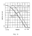
- Figs. 11 and 12 shows the simulation results of the frequency characteristic of the insertion loss and isolation in each of three cases, a first and a second one of which are the cases where externally attached inductors for resonance are used and not used in the circuit shown in Fig. 8 respectively, and a third one of which is the case where such a shunt FET as shown in Fig. 10 is used.
- the inductance of the resonance inductors L31 to L34 is set to 35 nH so as to have a resonance point at 1.5 GHz.
- Each of the FET31 to FET38 is constituted by a GaAs junction FET having a gate width of 1 mm, a gate length of 0.5 ⁇ m, and a pinch-off voltage of -0.5 V.
- the gate control voltage of these FET31 to FET38 is such that the on-bias voltage is 4 V, the off-bias voltage is 0 V, and the bias V bias is 3 V.
- the insertion loss in the case of Fig. 8 using the resonance inductors is superior centering 1.5 GHz to the case of using no inductor.
- the isolation is greatly improved in the case of using resonance inductors, and performance equivalent to or beyond that in the system of using a shunt FET is exhibited in the vicinity of 1.5 GHz.
- the drain and source terminals of the field-effect transistor in which the path between the drain and source thereof is made to be a signal path, are directly connected to the input/output terminals.
- the present invention is not limited to this but can be applied to the case where high impedance elements for application of a DC bias are connected to the drain and source terminals.
- the high impedance elements may be provided inside the IC chip or provided at a part of the IC chip or entirely outside the latter.
- This technique may be applied to the case of an SPST switching circuit, the case of an SPDP switching circuit, and the case of a DPDT switching circuit.
- the above technique may be applied, not only to the cases mentioned above, but also to the case where any one of or any combination of the FET switching control terminals, the FET drain and source biasing terminals, and the DC/RF grounding terminals is provided in the IC chip.
- the inductors L21 and L22 are externally provided outside the IC chip even between the input/output terminals RF1 and RF2 and between the RF1 and RF3.
- the present invention is not limited to this but an inductor may be connected between the input/output terminals RF2 and RF3.
- single-gate FETs are used.
- present invention is not limited to this but multi-gate FETs, such as dual-gate FETs may be used.
- one stage of FET is connected between every input and output terminals.
- the present invention is not limited to this but can be applied to the case where a plurality of stages of FETs are connected in series.
- junction FETs are used.
- the present invention is not limited to this but can be applied to the case of using MESFETS.
- an inductor is connected outside in parallel with the path between the drain and source of each of the field-effect transistors built in a switching integrated circuit, and the inductor and the OFF capacitance of the field-effect transistor are made to generate parallel resonance, so that it is possible to realize a switching circuit in which low insertion loss and sufficient isolation can be ensured at a desired frequency at the same time.
Landscapes
- Engineering & Computer Science (AREA)
- Computer Networks & Wireless Communication (AREA)
- Signal Processing (AREA)
- Electronic Switches (AREA)
- Transceivers (AREA)
- Waveguide Switches, Polarizers, And Phase Shifters (AREA)
Abstract
Description
- The present invention relates to a switching circuit, and more particularly to an improvement of a switching circuit which is preferably to be used for switching an input/output of a high frequency signal.
- Recently, mobile communication systems such as a mobile telephone system, a pocket telephone, and so on, have been developed as business on a large scale. On the other hand, shortage of communication circuits is getting more and more serious in city areas, and various mobile communication systems are coming into practical use in various countries. Non analog communication systems but digital communication systems are often adopted as these communication systems, and, as for a communication frequency band, a submicrowave band is used which is on the higher frequency side than that in current mobile communication systems.
- Semiconductor field-effect transistors (FET) are often used in a signal processing portion of a portable terminal in such a communication system which transmits and receives signals of a submicrowave band. Particularly, in the case of a portable terminal in which portability is regarded as important, it is regarded as important to develop a monolithic microwave IC (hereinafter abbreviated to 'MMIC) using a GaAs-FET, by which the portable terminal can be made small in size, low in driving voltage and low in power consumption. Particularly, a high-frequency switching device for switching a high-frequency signal in a portable terminal is becoming a key device.
- In most mobile communication systems which have come into use, digital systems are adopted as mentioned above. Of those digital systems, a TDMA (Time Division Multiple Access) system is often used. In this TDMA system, a communication band is divided by a predetermined time unit, and the divisional time sections are distributed to transmission, reception and another circuit. In the terminal side, therefore, in order to prevent transmission and reception from being conducted simultaneously, a switching circuit is often used for switching an antenna terminal between a transmission portion (Tx) and a reception portion (Rx).
- An example of such a communication terminal device is shown in Fig. 1. When there is much loss of a transmission signal W1 or a reception signal W2 in this switching circuit SW, the quality of the signal deteriorates correspondingly. To avoid this deterioration, it is necessary to increase the signal power correspondingly to the loss. It is therefore preferable to make the loss in the switching circuit SW as small as possible.
- In addition, there is a possibility that devices of the
reception portion 3 are broken if a transmission signal W1 leaks by a large quantity to the reception side. In addition, if the isolation between thetransmission portion 4 and thereception portion 3 is insufficient, signals may be distorted. It is therefore necessary to provide enough isolation between thetransmission portion 3 and thereception portion 4. Since superior high-frequency characteristic and high speed switching are thus required of the switching circuit SW, GaAs-FETs are often used as switching devices. - When a FET is used as a switching device, a gate bias which is much higher than a pinch-off voltage of the FET is applied to the gate of the FET so as to make the impedance low between the drain and source to thereby control the FET to be into an ON state. On the contrary, a gate bias which is much lower than the pinch-off voltage of the FET is applied to the gate so as to make the drain-source impedance high to thereby control the FET to an OFF state.
- In the case of a GaAs-FET available on the market recently, the FET can approximate a resistance component connected between the drain and source in an ON state while the FET can approximate a capacitance component connected between the drain and source in an OFF state. In this case, the resistance value and capacitance value of the FET can be regarded as several n/mm and several hundred fF/mm per gate width (Wg) of the FET, respectively. For example, the resistance Ron is 2 n/mm, and the capacitance Coff is 300 fF/mm.
- When a submicrowave signal is switched by use of just one such FET, there cannot be provided enough isolation if loss is restrained sufficiently. On the other hand, if enough isolation is ensured, loss is increased. That is, in order to realize a sufficiently small insertion loss, it is necessary to increase the gate width of the FET to a some extent so as to reduce the ON-resistance. On the other hand, the capacitance between the drain and source at the time of OFF is increased when the gate width is increased, so that there is a fear that the isolation deteriorates.
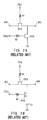
- Therefore, when a microwave signal is switched, often a FET1 is disposed in series with respect to a signal path, and a FET2 is disposed in a shunt position between the signal path and the ground, as shown in Fig. 2A. For example, when a signal band is 2 GHz, insertion loss of 1 dB or less and isolation of 20 dB or more can be easily ensured by a switching circuit constituted by a GaAs-FET disposed in such a series position and a GaAs-FET disposed in such a shunt position.
- When a FET is disposed in a shunt position as shown in Fig. 2A, the shunt FET is connected to the ground, so that the potential in each of the drain region and the source region of the FET is 0 V in DC so long as the FET is not separated in view of DC by a capacitor or the like as shown in Fig. 2B. Generally speaking, in order to turn a GaAs-FET off sufficiently, it is necessary to apply negative gate bias to the drain region and the source region.
- Therefore, a negative power supply is required to control the FET. However, if such a switching circuit is used as a terminal of a cellular communication or a portable telephone as mentioned above, the negative power supply needs a DC-DC converter, and so on, which is disadvantageous from the point of view of cost, size and power consumption. Therefore, a device using no negative power supply is being envisaged for a GaAs monolithic microwave IC (hereinafter abbreviated to 'MMIC') at present.
- In the case of this IC, a capacitance is provided between a shunt FET and the ground in a chip, and a FET in a switching circuit is isolated from the ground in view of DC. However, in this case, the capacitance provided for DC cut is considerably large in size in a submicrowave region. It is therefore disadvantageous in producing an inexpensive IC.
- In the case of a switching circuit for switching a signal among several places by means of FETs, such as an SPDT (Single Pole Dual Throw) switching circuit, there is a problem that insertion loss cannot be reduced to a certain value or less even if the size of isolation is ignored.
- This will be described in an SPDT switching circuit in Fig. 3. For example, the signal path between RF1 and RF2 is in an ON state (that is, a FET1 is in an ON state and a FET2 is in an OFF state), a signal passing the signal path between RF1 and RF2 leaks through an OFF capacitance Cds of the FET2 which is in an OFF state, so that the insertion loss deteriorates.
- Therefore, in the case where the gate width of the FET1 is made to be equal to that of the FET2, even if their gate widths are increased to reduce ON resistance of one FET which is in an ON state so as to reduce the signal loss of the FET which is in an ON state, the OFF capacitance Cds of the other FET which is in an OFF state increases to thereby increase the signal leaking from the FET in an OFF state, so that the insertion loss is not reduced beyond a certain value.
- Therefore, in the switching circuit for switching a signal among a plurality of directions by use of FETs as shown in Fig. 3 (other than an SPST (Single Pole Single Throw) switching device which is an ON/OFF switch, there is a limit also in reducing insertion loss.
- In view of the foregoing, an object of the present invention is to provide a switching circuit in which a desired-frequency microwave signal can be switched with low insertion loss and with high isolation.
- The foregoing object and other objects of the present invention have been achieved by the provision of a switching circuit comprising: a switching integrated circuit including a field-effect transistor having a signal path between a drain and a source, a high-impedance element connected to a gate terminal of the field-effect transistor, and first and second input/output terminals connected to a drain terminal and a source terminal of the field-effect transistor respectively; and an inductor provided outside the switching integrated circuit, and connecting the first and second input/output terminals to each other.
- Further, in the present invention, there is provided a switching circuit comprising: a switching integrated circuit including first, second and third input/output terminals, a first field-effect transistor having drain and source terminals connected to the first and second input/output terminals respectively, a second field-effect transistor having drain and source terminals connected to the first and third input/output terminals respectively, and first and second high-impedance elements connected to gate terminals of the first and second field-effect transistors respectively; and first and second inductors provided outside the switching integrated circuit, and connecting the first and second input/output terminals to each other, and the first and third input/output terminals to each other.
- Further, in the present invention, there is provided a switching circuit comprising: a switching integrated circuit including first, second, third and fourth input/output terminals, a first field-effect transistor having drain and source terminals connected to the first and second input/output terminals respectively, a second field-effect transistor having drain and source terminals connected to the second and third input/output terminals respectively, a third field-effect transistor having drain and source terminals connected to the third and fourth input/output terminals respectively, a fourth field-effect transistor having drain and source terminals connected to the fourth and first input/output terminals respectively, and first, second, third and fourth high-impedance elements connected to gate terminals of the first, second, third and fourth field-effect transistors respectively; and first, second, third and fourth inductors provided outside the switching integrated circuit, and connecting the first and second input/output terminals to each other, the second and third input/output terminals to each other, the third and fourth input/output terminals to each other, and the fourth and first input/output terminals to each other respectively.
- Even when the gate width of a field-effect transistor is increased to make loss insertion low, parallel resonance at a desired frequency is produced by the inductor externally connected in parallel with the path between the drain and source of the field-effect transistor and the OFF capacitance of the field-effect transistor, so that sufficient isolation can be ensured.
- The nature, principle and utility of the invention will become more apparent from the following detailed description when read in conjunction with the accompanying drawings in which like parts are designated by like reference numerals or characters.
- In the accompanying drawings :
- Fig. 1 is a block diagram explaining a basic communication terminal device;
- Figs. 2A and 2B are connection diagrams illustrating the configuration of a conventional switching circuit;
- Fig. 3 is a connection diagram illustrating a conventional configuration of an SPDT switching circuit;
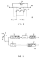
- Fig. 4 is a connection diagram illustrating an embodiment of an SPST switching circuit according to the present invention;
- Fig. 5 is a block diagram illustrating a communication terminal apparatus using the SPST switching circuit according to the present invention;
- Fig. 6 is a connection diagram illustrating an embodiment of an SPDT switching circuit according to the present invention;
- Fig. 7 is a block diagram illustrating a communication terminal apparatus using the SPDT switching circuit according to the present invention;
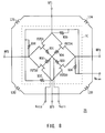
- Fig. 8 is a connection diagram illustrating an embodiment of a DPDT switching circuit according to the present invention;
- Fig. 9 is a block diagram illustrating a communication terminal apparatus using the DPDT switching circuit according to the present invention;
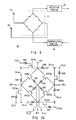
- Fig. 10 is a connection diagram illustrating an embodiment of a DPDT switching circuit to which a shunt FET is attached;
- Fig. 11 is a characteristic curve showing the frequency dependency of the insertion loss; and
- Fig. 12 is a characteristic curve showing the frequency dependency of the isolation.
- Preferred embodiments of the present invention will be described with reference to the accompanying drawings :
- Fig. 4 shows an SPST (Single Pole Single Throw) switching
circuit 11. ThisSPST switching circuit 11 is constituted by an integrated circuit (IC) and an inductor L11 connected in parallel with a signal line in the integrated circuit (IC). This switching circuit has a feature in that the inductor L11 is attached outside the integrated circuit. - The integrated circuit (IC) is constituted by a GaAs junction FET FET11 disposed at a position in series position with the signal path, a resistance R11 connected to a gate terminal of the FET11, and bias resistors R12 and R13 connected to a drain terminal and a source terminal of the FET11, respectively.
- The drain terminal and source terminal of the FET11, the gate bias resistor R11 and the bias resistors R12 and R13 are connected to terminals RF1, RF2, Vct1 and Vbias, all of which are provided outside the IC.
- By using only one FET, it is generally difficult to provide superior insertion loss and isolation at the same time.
- In the case of the
SPST switching circuit 11, however, since the inductor L11 is externally attached in parallel with the path between the drain and source, parallel resonance can be produced at a desired frequency between the OFF capacitance Coff existing between the drain and source of the FET and the inductance of the externally attached inductor L11 even if the gate width of the FET is increased to make the insertion loss low. Accordingly, it is understood that sufficient isolation can be ensured while keeping low insertion loss if theSPST switching circuit 11 is used. - In addition, in the case of the
SPST switching circuit 11, in comparison with such a switching circuit (Fig. 2B) in which a capacitor is provided between a shunt FET and the ground, the chip size can be reduced by the areas to be occupied by the shunt FET and the capacitor. Accordingly, it is possible to reduce the cost of manufacture. - In addition, because the inductor L11 is attached outside the IC chip, the inductance can be selected in accordance with a desired frequency and the property of general use can be also improved.
- Further, it can be considered to provide the inductor L11 inside the IC chip. In the case of attaching the inductor L11 outside the IC chip, however, the chip size can be reduced by the area of the inductor L11 in comparison with the case of providing the inductor L11 inside the IC chip, and the cost can be therefore reduced correspondingly.
- In addition, because of employing such an IC structure, the switching circuit can be made small in size and low in cost in comparison with the case where an equivalent circuit is constituted by discrete parts. Further, in this case, because the configuration of bias lines and so on is simple, it is easy to improve the performance.
- Next, Fig. 5 shows a circuit configuration where this
SPST switching circuit 11 is applied to an antenna switching circuit for use in a TDMA communication system. In this example, theSPST switching circuit 11 the transmission frequency of which is a resonance frequency is disposed between anantenna 2 and atransmission portion 12. In addition, a distributedconstant line 14 of 1/4 wavelength of the transmission frequency and aband pass filter 15 of reception frequency are disposed between theantenna 2 and areception portion 13. - In the thus configured circuit, control can be made so that enough isolation with respect to the transmission frequency can be obtained between the
antenna 2 and thereception portion 13 while signals of the reception frequency can be passed therebetween. - In the above configuration, the operation of transmission and reception of a
communication terminal device 16 will be described. First, at the time of transmission, theSPST switching circuit 11 is turned ON. Since enough isolation with respect to the transmission frequency is ensured between theantenna 2 and thereception portion 13 at this time, theantenna 2 is connected to thetransmission portion 12. - At the time of reception, on the contrary, the
SPST switching circuit 11 is turned OFF. Since enough isolation with respect to the reception frequency is ensured between theantenna 2 and thetransmission portion 12 at this time, the path between theantenna 2 and thereception portion 13 is conductive so that theantenna 2 is connected to thereception portion 13. - When the
SPST switching circuit 11 is used in a TDMA communication switching circuit in this manner, it is possible to obtain such acommunication terminal device 16 in which theantenna 2 can be switched between the transmission and reception portions alternatively while low insertion loss and high isolation are realized, and which is superior in speech property, small in size and low in cost. - Next, Fig. 6 shows an SPDT (Single Pole Dual Throw) switching
circuit 21 arranged according to the same principle as that in the first embodiment. - Also in this
SPDT switching circuit 21, the OFF capacitances Coff between the drain and source of a GaAs junction FET FET21 and the drain and source of a FET22 in an IC chip, and the inductances of inductors L21 and L22 attached outside the IC chip are made to generate parallel resonance so as to ensure low insertion loss and isolation sufficiently. - In addition, there is a limit in such a circuit as shown in Fig. 3 even if isolation is ignored to reduce insertion loss. In the circuit shown in Fig. 6, however, the isolation of signal lines in an OFF state can be ensured ideally by the externally attached inductors L21 and L22 even if the gate width of the FETs is enlarged (that is, signals can be restrained from leaking from the signal lines), so that lower insertion loss than that of the circuit shown in Fig. 3 can be realized.
- Next, Fig. 7 shows a circuit configuration where the thus configured
SPDT switching circuit 21 is applied to an antenna switching circuit for a TDMA communication system. - When the
SPDT switching circuit 21 is used for a TDMA communication switching circuit in such a manner, it is possible to obtain acommunication terminal device 24 in which anantenna 2 can be switched between transmission and reception portions alternatively while low insertion loss and high isolation are realized, and which is superior in speech property, small in size and low in cost. - Finally, a DPDT (Dual Pole Dual Throw) switching
circuit 31 configured in accordance with the same principle as that in the first embodiment is shown in Fig. 8. - Also in this
DPDT switching circuit 31, the OFF capacitances Coff between the drain and source of GaAs junction FETs FET31 to FET34 in an IC and inductors L31 to L34 attached outside are made to resonate in parallel, so as to ensure low insertion loss and isolation sufficiently. - In addition, in the circuit where a plurality of signal lines (two, in this case) are connected to another signal line, insertion loss can be effectively prevented from deteriorating in comparison with the case of Fig. 6. That is, when parallel resonance is not used, the number of FETs which are in an OFF state is increased (because parasitic capacitance causing signals to leak is increased), so that the deterioration of the insertion loss is largcr than that in Fig. 6. Therefore, if parallel resonance is used, there is ideally no signal leakage from the FETs which are in an OFF state, so that it is possible to obtain insertion loss equivalent to that of an SPST switching circuit.
- Next, Fig. 9 shows a circuit configuration where the thus configured
DPDT switching circuit 31 is applied to an antenna switching circuit for a TDMA communication system. In this example, aninside antenna 2A and anoutside antenna 2B are provided in a terminal, and each of the antennae is switched between atransmission portion 32 and areception portion 33. - When the
DPDT switching circuit 31 is used for a TDMA communication switching circuit in this manner, it is possible to obtain such acommunication terminal device 34 in which each of theantennae - Next, actual examples of the effects of the
communication terminal device 34 are shown. Fig. 10 is a circuit diagram of a switching circuit where isolation is ensured by use of a shunt FET. Figs. 11 and 12 shows the simulation results of the frequency characteristic of the insertion loss and isolation in each of three cases, a first and a second one of which are the cases where externally attached inductors for resonance are used and not used in the circuit shown in Fig. 8 respectively, and a third one of which is the case where such a shunt FET as shown in Fig. 10 is used. - The inductance of the resonance inductors L31 to L34 is set to 35 nH so as to have a resonance point at 1.5 GHz. Each of the FET31 to FET38 is constituted by a GaAs junction FET having a gate width of 1 mm, a gate length of 0.5 µm, and a pinch-off voltage of -0.5 V. The gate control voltage of these FET31 to FET38 is such that the on-bias voltage is 4 V, the off-bias voltage is 0 V, and the bias Vbias is 3 V.
- As seen from Fig. 11, the insertion loss in the case of Fig. 8 using the resonance inductors is superior centering 1.5 GHz to the case of using no inductor. Further, also as for the isolation, as shown in Fig. 12, the isolation is greatly improved in the case of using resonance inductors, and performance equivalent to or beyond that in the system of using a shunt FET is exhibited in the vicinity of 1.5 GHz.
- In the above embodiments, the drain and source terminals of the field-effect transistor, in which the path between the drain and source thereof is made to be a signal path, are directly connected to the input/output terminals. However, the present invention is not limited to this but can be applied to the case where high impedance elements for application of a DC bias are connected to the drain and source terminals. The high impedance elements may be provided inside the IC chip or provided at a part of the IC chip or entirely outside the latter.
- This technique may be applied to the case of an SPST switching circuit, the case of an SPDP switching circuit, and the case of a DPDT switching circuit.
- The above technique may be applied, not only to the cases mentioned above, but also to the case where any one of or any combination of the FET switching control terminals, the FET drain and source biasing terminals, and the DC/RF grounding terminals is provided in the IC chip.
- Further, in the case of the SPDT switching circuit in the above embodiments, the inductors L21 and L22 are externally provided outside the IC chip even between the input/output terminals RF1 and RF2 and between the RF1 and RF3. However, the present invention is not limited to this but an inductor may be connected between the input/output terminals RF2 and RF3.
- Further, in the above embodiments, single-gate FETs are used. However, the present invention is not limited to this but multi-gate FETs, such as dual-gate FETs may be used.
- Further, in the above embodiments, one stage of FET is connected between every input and output terminals. However, the present invention is not limited to this but can be applied to the case where a plurality of stages of FETs are connected in series.
- In the above embodiments, junction FETs are used. However, the present invention is not limited to this but can be applied to the case of using MESFETS.
- As has been described above, according to the present invention, an inductor is connected outside in parallel with the path between the drain and source of each of the field-effect transistors built in a switching integrated circuit, and the inductor and the OFF capacitance of the field-effect transistor are made to generate parallel resonance, so that it is possible to realize a switching circuit in which low insertion loss and sufficient isolation can be ensured at a desired frequency at the same time.
- While there has been described in connection with the preferred embodiments of the invention, it will be obvious to those skilled in the art that various changes and modifications may be aimed, therefore, to cover in the appended claims.
Claims (22)
- A switching circuit comprising :a switching integrated circuit (IC) includinga field-effect transistor (FET11) having a signal path between a drain and a source,a high-impedance element (R11) connected to a gate terminal of said field-effect transistor, andfirst and second input/output terminals (RF1, RF2) connected to a drain terminal and a source terminal of said field-effect transistor respectively; andan inductor (L11) connecting said first and second input/output terminals to each other.
- The switching circuit according to claim 1, wherein said inductor (L11) is provided outside said switching integrated circuit (IC).
- The switching circuit according to claim 1, wherein a part of or all of input/output terminals (Vbias, Vct1) inside or outside said switching integrated circuit (IC) are connected to a high-impedance element (R12, R13) for applying a predetermined DC bias to the drain and source terminals of said field-effect transistor/transistors (FET 11).
- The switching circuit (11) according to claim 1, wherein said switching integrated circuit (IC) has a part of or all of a control terminal used for switching control of said field-effect transistor/transistors, a bias terminal (Vbias, Vct1) for applying a predetermined bias to the drain and source terminals of said field-effect transistor/transistors (FET11), and a DC or AC ground terminal.
- The switching circuit according to claim 1, wherein said field-effect transistor/transistors (FET11) are constituted by multi-gate field-effect transistor/transistors.
- The switching circuit according to claim 1, wherein a plurality of stages of field-effect transistors (FET21, FET22) are connected in series in a portion of said field-effect transistor/transistors.
- The switching circuit according to claim 1, wherein said field-effect transistor/transistors (FET11; FET21, FET22) is/are a junction field-effect transistor/transistors.
- A switching circuit comprising :a switching integrated circuit (IC) includingfirst, second and third input/output terminals (RF1, RF2, RF3),a first field-effect transistor (FET21) having drain and source terminals connected to said first and second input/output terminals respectively,a second field-effect transistor (FET22) having drain and source terminals connected to said first and third input/output terminals respectively, andfirst and second high-impedance elements (R21, R22) connected to gate terminals of said first and second field-effect transistors respectively; andfirst and second inductors (L21, L22) connecting said first and second input/output terminals to each other and said first and third input/output terminals to each other respectively.
- The switching circuit according to claim 8, wherein said inductors (L21, L22) are provided outside said switching integrated circuit (IC).
- The switching circuit according to claim 8, further comprising :
a third inductor (L32) provided outside said switching integrated circuit (IC) and connecting said second and third input/output terminals (RF2, RF3) to each other. - The switching circuit according to claim 8, wherein a part of or all of said input/output terminals (RF1-3) inside or outside said switching integrated circuit (IC) are connected to a high-impedance element (R23, R24, R25) for applying a predetermined DC bias (Vbias) to the drain and source terminals of said field-effect transistor/transistors (FET21, FET22).
- The switching circuit according to claim 8, wherein said switching integrated circuit (IC) has a part of or all of a control terminal (Vctl1, Vctl2) used for switching control of said field-effect transistor/transistors (FET21, FET22), a bias terminal (Vbias) for applying a predetermined bias to the drain and source terminals of said field-effect transistor/transistors, and a DC or AC ground terminal.
- The switching circuit according to claim 8, wherein said field-effect transistor/transistors (FET21, FET22) are constituted by multi-gate field-effect transistor/transistors.
- The switching circuit according to claim 8, wherein a plurality of stages of field-effect transistors are connected in series in a portion of said field-effect transistor/transistors.
- The switching circuit according to claim 8, wherein said field-effect transistor/transistors is/are a junction field-effect transistor/transistors.
- A switching circuit comprising :a switching integrated circuit (IC) including first, second, third and fourth input/output terminals (RF1-RF4),a first field-effect transistor (FET31) having drain and source terminals connected to said first and second input/output terminals respectively,a second field-effect transistor (FET32) having drain and source terminals connected to said second and third input/output terminals respectively,a third field-effect transistor (FET33) having drain and source terminals connected to said third and fourth input/output terminals respectively,a fourth field-effect transistor (FET34) having drain and source terminals connected to said fourth and first input/output terminals respectively, andfirst, second, third and fourth high-impedance elements (R31-R34) connected to gate terminals of said first, second, third and fourth field-effect transistors respectively; andfirst, second, third and fourth inductors (L31-L34) connecting said first and second input/output terminals to each other, said second and third input/output terminals to each other, said third and fourth input/output terminals to each other, and said fourth and first input/output terminals to each other respectively.
- The switching circuit according to claim 16, wherein said inductors (L31-L34) are provided outside said switching integrated circuit (IC).
- The switching circuit according to claim 16, wherein a part of or all of said input/output terminals (RF1-RF4) are inside or outside said switching integrated circuit (IC) and are connected to a respective high-impedance element (R35-R38) for applying a predetermined DC bias to the drain and source terminals of said field-effect transistor/transistors (FET31-FET34).
- The switching circuit according to claim 16, wherein said switching integrated circuit has a part of or all of a control terminal (Vctl1, Vctl2) used for switching control of said field-effect transistor/transistors (FET31-FET32), a bias terminal for applying a predetermined bias to the drain and source terminals of said field-effect transistor/transistors, and a DC or AC ground terminal.
- The switching circuit according to claim 16, wherein said field-effect transistor/transistors (FET31-FET34) are constituted by multi-gate field-effect transistor/transistors.
- The switching circuit according to claim 16, wherein a plurality of stages of field-effect transistors are connected in series in a portion of said field-effect transistor/transistors.
- The switching circuit according to claim 16, wherein said field-effect transistor/transistors is/are a junction field-effect transistor/transistors (FET31-FET34).
Applications Claiming Priority (3)
| Application Number | Priority Date | Filing Date | Title |
|---|---|---|---|
| JP7027309A JPH08204530A (en) | 1995-01-23 | 1995-01-23 | Switch circuit |
| JP2730995 | 1995-01-23 | ||
| JP27309/95 | 1995-01-23 |
Publications (3)
| Publication Number | Publication Date |
|---|---|
| EP0723338A2 true EP0723338A2 (en) | 1996-07-24 |
| EP0723338A3 EP0723338A3 (en) | 1996-12-11 |
| EP0723338B1 EP0723338B1 (en) | 2000-04-19 |
Family
ID=12217494
Family Applications (1)
| Application Number | Title | Priority Date | Filing Date |
|---|---|---|---|
| EP96400158A Expired - Lifetime EP0723338B1 (en) | 1995-01-23 | 1996-01-23 | Switching circuit |
Country Status (4)
| Country | Link |
|---|---|
| US (2) | US5825227A (en) |
| EP (1) | EP0723338B1 (en) |
| JP (1) | JPH08204530A (en) |
| DE (1) | DE69607773T2 (en) |
Cited By (9)
| Publication number | Priority date | Publication date | Assignee | Title |
|---|---|---|---|---|
| WO1998037640A1 (en) * | 1997-02-24 | 1998-08-27 | At & T Wireless Services, Inc. | Transmit/receive switch |
| EP0893882A3 (en) * | 1997-07-25 | 2001-02-14 | Kabushiki Kaisha Toshiba | High frequency switch device, front end unit and transceiver |
| EP0911985A3 (en) * | 1997-10-21 | 2002-10-02 | Matsushita Electric Industrial Co., Ltd. | Dual band Transmitter with switchable matching circuit |
| EP0827286A3 (en) * | 1996-08-29 | 2003-05-21 | Philips Intellectual Property & Standards GmbH | Ring switch for telecommunication apparatus |
| EP1156530A3 (en) * | 2000-05-15 | 2005-05-11 | Sanyo Electric Co., Ltd. | Compound semiconductor switching device for high frequency switching |
| WO2007123822A2 (en) | 2006-04-17 | 2007-11-01 | Skyworks Solutions, Inc. | High-frequency switching device with reduced harmonics |
| WO2015151067A1 (en) * | 2014-04-03 | 2015-10-08 | Teko Telecom S.R.L. | Radio frequency switching system |
| US10027366B2 (en) | 2014-04-25 | 2018-07-17 | Raytheon Company | High power radio frequency (RF) antenna switch |
| CN108574479A (en) * | 2017-03-08 | 2018-09-25 | 康希通信科技(上海)有限公司 | Single-pole single-throw(SPST RF switch and its hilted broadsword of composition throw RF switch more |
Families Citing this family (93)
| Publication number | Priority date | Publication date | Assignee | Title |
|---|---|---|---|---|
| EP1909390A2 (en) * | 1996-09-26 | 2008-04-09 | Matsushita Electric Industrial Co., Ltd. | Diplexer, duplexer, and two-channel mobile communications equipment |
| JPH10150387A (en) * | 1996-11-18 | 1998-06-02 | Nec Corp | Hot standby changeover device |
| JPH1188004A (en) | 1997-09-03 | 1999-03-30 | Mitsubishi Electric Corp | Microwave circuit |
| US5990580A (en) * | 1998-03-05 | 1999-11-23 | The Whitaker Corporation | Single pole double throw switch |
| FR2781949B1 (en) * | 1998-08-03 | 2000-10-27 | St Microelectronics Sa | RADIO FREQUENCY SIGNAL SWITCHING DEVICE |
| JP2000114950A (en) * | 1998-10-07 | 2000-04-21 | Murata Mfg Co Ltd | SPST switch, SPDT switch and communication device using the same |
| US6052019A (en) * | 1998-10-29 | 2000-04-18 | Pericom Semiconductor Corp. | Undershoot-isolating MOS bus switch |
| US6396325B2 (en) * | 1999-12-03 | 2002-05-28 | Fairchild Semiconductor Corporation | High frequency MOSFET switch |
| JP3637830B2 (en) * | 2000-02-22 | 2005-04-13 | 株式会社村田製作所 | SPDT switch and communication device using the same |
| US6351628B1 (en) | 2000-03-06 | 2002-02-26 | Motorola, Inc. | Antenna switching circuit |
| US6580107B2 (en) | 2000-10-10 | 2003-06-17 | Sanyo Electric Co., Ltd. | Compound semiconductor device with depletion layer stop region |
| JP2002135095A (en) * | 2000-10-26 | 2002-05-10 | Nec Kansai Ltd | IC switch |
| JP3736356B2 (en) * | 2001-02-01 | 2006-01-18 | 日本電気株式会社 | High frequency switch circuit |
| JP2002289790A (en) | 2001-03-27 | 2002-10-04 | Sanyo Electric Co Ltd | Compound semiconductor switch circuit device |
| TW530455B (en) | 2001-04-19 | 2003-05-01 | Sanyo Electric Co | Switch circuit device of compound semiconductor |
| JP2003086767A (en) * | 2001-09-14 | 2003-03-20 | Matsushita Electric Ind Co Ltd | Semiconductor device |
| US6489856B1 (en) * | 2001-09-17 | 2002-12-03 | Tyco Electronics Corporation | Digital attenuator with combined bits |
| US6804502B2 (en) | 2001-10-10 | 2004-10-12 | Peregrine Semiconductor Corporation | Switch circuit and method of switching radio frequency signals |
| KR100974107B1 (en) * | 2002-02-25 | 2010-08-04 | 엔엑스피 비 브이 | Electronic signal processing unit and electronic signal switch |
| US6774718B2 (en) * | 2002-07-19 | 2004-08-10 | Micro Mobio Inc. | Power amplifier module for wireless communication devices |
| US20040232982A1 (en) * | 2002-07-19 | 2004-11-25 | Ikuroh Ichitsubo | RF front-end module for wireless communication devices |
| US7071783B2 (en) * | 2002-07-19 | 2006-07-04 | Micro Mobio Corporation | Temperature-compensated power sensing circuit for power amplifiers |
| US7493094B2 (en) * | 2005-01-19 | 2009-02-17 | Micro Mobio Corporation | Multi-mode power amplifier module for wireless communication devices |
| US6730953B2 (en) * | 2002-09-13 | 2004-05-04 | Mia-Com, Inc. | Apparatus, methods and articles of manufacture for a low control voltage switch |
| US6803680B2 (en) * | 2002-09-13 | 2004-10-12 | Mia-Com, Inc. | Apparatus, methods, and articles of manufacture for a switch having sharpened control voltage |
| US6900711B2 (en) * | 2002-09-30 | 2005-05-31 | Agilent Technologies, Inc. | Switching system |
| US6903596B2 (en) * | 2003-03-17 | 2005-06-07 | Mitsubishi Electric & Electronics U.S.A., Inc. | Method and system for impedance matched switching |
| DE10313868B4 (en) * | 2003-03-21 | 2009-11-19 | Siemens Ag | Catheter for magnetic navigation |
| JP3790227B2 (en) * | 2003-04-16 | 2006-06-28 | 松下電器産業株式会社 | High frequency switch circuit |
| JP2005006072A (en) * | 2003-06-12 | 2005-01-06 | Matsushita Electric Ind Co Ltd | High frequency switch device and semiconductor device |
| US20050205986A1 (en) * | 2004-03-18 | 2005-09-22 | Ikuroh Ichitsubo | Module with integrated active substrate and passive substrate |
| JP4321359B2 (en) * | 2004-05-31 | 2009-08-26 | パナソニック株式会社 | Semiconductor switch |
| US7221207B2 (en) * | 2004-06-04 | 2007-05-22 | Matsushita Electric Industrial Co., Ltd. | Semiconductor switching circuit for switching the paths of a high frequency signal in a mobile communications unit |
| WO2006002347A1 (en) | 2004-06-23 | 2006-01-05 | Peregrine Semiconductor Corporation | Integrated rf front end |
| US7254371B2 (en) * | 2004-08-16 | 2007-08-07 | Micro-Mobio, Inc. | Multi-port multi-band RF switch |
| JP2006121187A (en) * | 2004-10-19 | 2006-05-11 | Toshiba Corp | Semiconductor switching circuit |
| US7262677B2 (en) * | 2004-10-25 | 2007-08-28 | Micro-Mobio, Inc. | Frequency filtering circuit for wireless communication devices |
| US7389090B1 (en) | 2004-10-25 | 2008-06-17 | Micro Mobio, Inc. | Diplexer circuit for wireless communication devices |
| JP4298636B2 (en) * | 2004-11-26 | 2009-07-22 | パナソニック株式会社 | High frequency switch circuit device |
| US7221225B2 (en) | 2004-12-03 | 2007-05-22 | Micro-Mobio | Dual band power amplifier module for wireless communication devices |
| US7548111B2 (en) * | 2005-01-19 | 2009-06-16 | Micro Mobio Corporation | Miniature dual band power amplifier with reserved pins |
| US7580687B2 (en) * | 2005-01-19 | 2009-08-25 | Micro Mobio Corporation | System-in-package wireless communication device comprising prepackaged power amplifier |
| US7084702B1 (en) * | 2005-01-19 | 2006-08-01 | Micro Mobio Corp. | Multi-band power amplifier module for wireless communication devices |
| US7769355B2 (en) * | 2005-01-19 | 2010-08-03 | Micro Mobio Corporation | System-in-package wireless communication device comprising prepackaged power amplifier |
| JP4763310B2 (en) * | 2005-02-22 | 2011-08-31 | 新日本無線株式会社 | Semiconductor switch integrated circuit |
| JP2006332778A (en) * | 2005-05-23 | 2006-12-07 | Matsushita Electric Ind Co Ltd | High frequency switch circuit and semiconductor device using the same |
| US7498862B2 (en) * | 2005-05-31 | 2009-03-03 | Texas Instruments Incorporated | Switch for handling terminal voltages exceeding control voltage |
| US8742502B2 (en) | 2005-07-11 | 2014-06-03 | Peregrine Semiconductor Corporation | Method and apparatus for use in improving linearity of MOSFETs using an accumulated charge sink-harmonic wrinkle reduction |
| US20080076371A1 (en) | 2005-07-11 | 2008-03-27 | Alexander Dribinsky | Circuit and method for controlling charge injection in radio frequency switches |
| US7890891B2 (en) | 2005-07-11 | 2011-02-15 | Peregrine Semiconductor Corporation | Method and apparatus improving gate oxide reliability by controlling accumulated charge |
| US9653601B2 (en) | 2005-07-11 | 2017-05-16 | Peregrine Semiconductor Corporation | Method and apparatus for use in improving linearity of MOSFETs using an accumulated charge sink-harmonic wrinkle reduction |
| USRE48965E1 (en) | 2005-07-11 | 2022-03-08 | Psemi Corporation | Method and apparatus improving gate oxide reliability by controlling accumulated charge |
| US7910993B2 (en) | 2005-07-11 | 2011-03-22 | Peregrine Semiconductor Corporation | Method and apparatus for use in improving linearity of MOSFET's using an accumulated charge sink |
| US20070063982A1 (en) * | 2005-09-19 | 2007-03-22 | Tran Bao Q | Integrated rendering of sound and image on a display |
| US7477204B2 (en) * | 2005-12-30 | 2009-01-13 | Micro-Mobio, Inc. | Printed circuit board based smart antenna |
| FR2902250A1 (en) * | 2006-06-12 | 2007-12-14 | Thomson Licensing Sas | SWITCH AND SELECTIVE ISOLATION SWITCHING DEVICE FOR MULTIMEDIA TERMINALS |
| US7477108B2 (en) * | 2006-07-14 | 2009-01-13 | Micro Mobio, Inc. | Thermally distributed integrated power amplifier module |
| JP4342569B2 (en) * | 2007-04-17 | 2009-10-14 | 株式会社東芝 | High frequency switch circuit |
| US7960772B2 (en) | 2007-04-26 | 2011-06-14 | Peregrine Semiconductor Corporation | Tuning capacitance to enhance FET stack voltage withstand |
| JP2009159059A (en) * | 2007-12-25 | 2009-07-16 | Samsung Electro Mech Co Ltd | High frequency switching circuit |
| WO2009108391A1 (en) | 2008-02-28 | 2009-09-03 | Peregrine Semiconductor Corporation | Method and apparatus for use in digitally tuning a capacitor in an integrated circuit device |
| US7786822B2 (en) * | 2008-05-27 | 2010-08-31 | Avago Technologies Wireless Ip (Singapore) Pte. Ltd. | Four-state digital attenuator having two-bit control interface |
| GB2465404A (en) * | 2008-11-18 | 2010-05-19 | Iti Scotland Ltd | Plural antenna elements with a switching arrangement and method |
| JP2010220200A (en) * | 2009-02-19 | 2010-09-30 | Renesas Electronics Corp | Conduction switching circuit, conduction switching circuit block, and operation method for conduction switching circuit |
| US8723260B1 (en) | 2009-03-12 | 2014-05-13 | Rf Micro Devices, Inc. | Semiconductor radio frequency switch with body contact |
| CN101938274B (en) * | 2009-06-30 | 2013-04-24 | 瀚宇彩晶股份有限公司 | Integrated gate drive circuit |
| CN102025357B (en) * | 2009-09-18 | 2012-06-13 | 富士迈半导体精密工业(上海)有限公司 | discharge circuit |
| WO2012038947A1 (en) * | 2010-09-21 | 2012-03-29 | Dsp Group Ltd. | Rf switch implementation in cmos process |
| CN101997529B (en) * | 2010-09-25 | 2012-09-12 | 林松 | Intelligent wiring-free learning code remote control switch |
| CN102035523B (en) * | 2011-01-12 | 2012-11-21 | 上海三基电子工业有限公司 | High-voltage heavy-current electronic switch |
| US9324512B2 (en) * | 2011-11-28 | 2016-04-26 | Nanyang Technological University | SPST switch, SPDT switch, SPMT switch and communication device using the same |
| KR20130127782A (en) * | 2012-05-15 | 2013-11-25 | 삼성전기주식회사 | A switching circuit and a wireless communication system including the same |
| JP2013247419A (en) * | 2012-05-24 | 2013-12-09 | Fujitsu Ltd | Amplifier, transmitter/receiver and communication device |
| JP5944813B2 (en) * | 2012-11-08 | 2016-07-05 | 太陽誘電株式会社 | Switching devices and modules |
| US9590674B2 (en) | 2012-12-14 | 2017-03-07 | Peregrine Semiconductor Corporation | Semiconductor devices with switchable ground-body connection |
| US20150236798A1 (en) | 2013-03-14 | 2015-08-20 | Peregrine Semiconductor Corporation | Methods for Increasing RF Throughput Via Usage of Tunable Filters |
| US9406695B2 (en) | 2013-11-20 | 2016-08-02 | Peregrine Semiconductor Corporation | Circuit and method for improving ESD tolerance and switching speed |
| JP2015170935A (en) * | 2014-03-06 | 2015-09-28 | 国立大学法人東北大学 | Sample-hold circuit, and high-frequency receiver |
| US9654094B2 (en) | 2014-03-12 | 2017-05-16 | Kabushiki Kaisha Toshiba | Semiconductor switch circuit and semiconductor substrate |
| GB2527638B (en) * | 2014-04-30 | 2019-03-27 | Skyworks Solutions Inc | Bypass path loss reduction |
| US9847804B2 (en) | 2014-04-30 | 2017-12-19 | Skyworks Solutions, Inc. | Bypass path loss reduction |
| US9831857B2 (en) | 2015-03-11 | 2017-11-28 | Peregrine Semiconductor Corporation | Power splitter with programmable output phase shift |
| US10097232B2 (en) * | 2016-06-08 | 2018-10-09 | Psemi Corporation | Apparatus for reducing RF crossover coupling |
| US10172231B2 (en) | 2016-06-08 | 2019-01-01 | Psemi Corporation | Methods and apparatus for reducing RF crossover coupling |
| US9948281B2 (en) | 2016-09-02 | 2018-04-17 | Peregrine Semiconductor Corporation | Positive logic digitally tunable capacitor |
| US10361697B2 (en) * | 2016-12-23 | 2019-07-23 | Skyworks Solutions, Inc. | Switch linearization by compensation of a field-effect transistor |
| US10910714B2 (en) | 2017-09-11 | 2021-02-02 | Qualcomm Incorporated | Configurable power combiner and splitter |
| US10505530B2 (en) | 2018-03-28 | 2019-12-10 | Psemi Corporation | Positive logic switch with selectable DC blocking circuit |
| US10886911B2 (en) | 2018-03-28 | 2021-01-05 | Psemi Corporation | Stacked FET switch bias ladders |
| US10236872B1 (en) | 2018-03-28 | 2019-03-19 | Psemi Corporation | AC coupling modules for bias ladders |
| US11069475B2 (en) | 2018-07-24 | 2021-07-20 | Psemi Corporation | Compact isolated inductors |
| US11476849B2 (en) | 2020-01-06 | 2022-10-18 | Psemi Corporation | High power positive logic switch |
| EP4354742A1 (en) * | 2022-10-12 | 2024-04-17 | Nokia Technologies Oy | Flexible reception |
Family Cites Families (16)
| Publication number | Priority date | Publication date | Assignee | Title |
|---|---|---|---|---|
| JPS5791334U (en) * | 1980-11-21 | 1982-06-05 | ||
| US4556808A (en) * | 1982-06-03 | 1985-12-03 | Texas Instruments Incorporated | Microwave monolithic spot FET switch configuration |
| US4789846A (en) * | 1986-11-28 | 1988-12-06 | Mitsubishi Denki Kabushiki Kaisha | Microwave semiconductor switch |
| US4975604A (en) * | 1987-05-29 | 1990-12-04 | Triquint Semiconductor, Inc. | Automatic return-loss optimization of a variable fet attenuator |
| GB2211987B (en) * | 1987-10-30 | 1992-01-02 | Plessey Co Plc | Circuit arrangement including an inductor and a mesfet |
| US4931753A (en) * | 1989-01-17 | 1990-06-05 | Ford Aerospace Corporation | Coplanar waveguide time delay shifter |
| US4890077A (en) * | 1989-03-28 | 1989-12-26 | Teledyne Mec | FET monolithic microwave integrated circuit variable attenuator |
| JPH0349401A (en) * | 1989-07-18 | 1991-03-04 | Mitsubishi Electric Corp | Microwave element |
| US5191338A (en) * | 1991-11-29 | 1993-03-02 | General Electric Company | Wideband transmission-mode FET linearizer |
| US5148062A (en) * | 1991-12-19 | 1992-09-15 | Raytheon Company | Simplified phase shifter circuit |
| JPH0697799A (en) * | 1992-09-10 | 1994-04-08 | Mitsubishi Electric Corp | Reflective switch |
| JPH06232601A (en) * | 1993-01-29 | 1994-08-19 | Mitsubishi Electric Corp | Microwave switch circuit |
| JP3191891B2 (en) * | 1993-04-21 | 2001-07-23 | 三菱電機株式会社 | 90 ° phase shifter |
| JP3243892B2 (en) * | 1993-05-21 | 2002-01-07 | ソニー株式会社 | Signal switch |
| JPH07303001A (en) * | 1994-05-10 | 1995-11-14 | Hitachi Ltd | High frequency switch |
| JP3249393B2 (en) * | 1995-09-28 | 2002-01-21 | 株式会社東芝 | Switch circuit |
-
1995
- 1995-01-23 JP JP7027309A patent/JPH08204530A/en active Pending
-
1996
- 1996-01-18 US US08/588,238 patent/US5825227A/en not_active Expired - Lifetime
- 1996-01-23 DE DE69607773T patent/DE69607773T2/en not_active Expired - Lifetime
- 1996-01-23 EP EP96400158A patent/EP0723338B1/en not_active Expired - Lifetime
-
1997
- 1997-10-24 US US08/957,463 patent/US5969560A/en not_active Expired - Lifetime
Cited By (13)
| Publication number | Priority date | Publication date | Assignee | Title |
|---|---|---|---|---|
| EP0827286A3 (en) * | 1996-08-29 | 2003-05-21 | Philips Intellectual Property & Standards GmbH | Ring switch for telecommunication apparatus |
| WO1998037640A1 (en) * | 1997-02-24 | 1998-08-27 | At & T Wireless Services, Inc. | Transmit/receive switch |
| US5909641A (en) * | 1997-02-24 | 1999-06-01 | At&T Wireless Services Inc. | Transmit/receive switch |
| EP0893882A3 (en) * | 1997-07-25 | 2001-02-14 | Kabushiki Kaisha Toshiba | High frequency switch device, front end unit and transceiver |
| EP0911985A3 (en) * | 1997-10-21 | 2002-10-02 | Matsushita Electric Industrial Co., Ltd. | Dual band Transmitter with switchable matching circuit |
| EP1156530A3 (en) * | 2000-05-15 | 2005-05-11 | Sanyo Electric Co., Ltd. | Compound semiconductor switching device for high frequency switching |
| WO2007123822A2 (en) | 2006-04-17 | 2007-11-01 | Skyworks Solutions, Inc. | High-frequency switching device with reduced harmonics |
| EP2008362A4 (en) * | 2006-04-17 | 2010-04-28 | Skyworks Solutions Inc | HIGH FREQUENCY TO REDUCED HARMONIC SWITCHING DEVICE |
| WO2015151067A1 (en) * | 2014-04-03 | 2015-10-08 | Teko Telecom S.R.L. | Radio frequency switching system |
| US9966987B2 (en) | 2014-04-03 | 2018-05-08 | Teko Telecom S.R.L. | Radio frequency switching system |
| US10027366B2 (en) | 2014-04-25 | 2018-07-17 | Raytheon Company | High power radio frequency (RF) antenna switch |
| CN108574479A (en) * | 2017-03-08 | 2018-09-25 | 康希通信科技(上海)有限公司 | Single-pole single-throw(SPST RF switch and its hilted broadsword of composition throw RF switch more |
| CN108574479B (en) * | 2017-03-08 | 2024-03-05 | 康希通信科技(上海)有限公司 | Single-pole single-throw radio frequency switch and its composed single-pole multi-throw radio frequency switch |
Also Published As
| Publication number | Publication date |
|---|---|
| EP0723338B1 (en) | 2000-04-19 |
| US5969560A (en) | 1999-10-19 |
| JPH08204530A (en) | 1996-08-09 |
| US5825227A (en) | 1998-10-20 |
| DE69607773T2 (en) | 2000-11-23 |
| DE69607773D1 (en) | 2000-05-25 |
| EP0723338A3 (en) | 1996-12-11 |
Similar Documents
| Publication | Publication Date | Title |
|---|---|---|
| EP0723338B1 (en) | Switching circuit | |
| JP3332194B2 (en) | Switch semiconductor integrated circuit and communication terminal device | |
| KR100389465B1 (en) | Switch circuit and composite switch circuit | |
| JP3441236B2 (en) | Semiconductor integrated circuit device | |
| EP0700161B1 (en) | Low distortion switch | |
| EP0766396B1 (en) | Switching circuit | |
| US6882829B2 (en) | Integrated circuit incorporating RF antenna switch and power amplifier | |
| US8676132B2 (en) | Semiconductor integrated circuit, RF module using the same, and radio communication terminal device using the same | |
| US5796286A (en) | Attenuation circuitry using gate current control of FET conduction to vary attenuation | |
| US7197284B2 (en) | Antenna switches including field effect transistors | |
| EP0903855B1 (en) | High frequency switching device | |
| JP2848502B2 (en) | Microwave semiconductor switch | |
| US20070290744A1 (en) | Radio frequency switching circuit, radio frequency switching device, and transmitter module device | |
| JPH07303001A (en) | High frequency switch | |
| JP2007067762A (en) | Semiconductor integrated circuit device and high frequency power amplification module | |
| US7671697B2 (en) | High-isolation switching device for millimeter-wave band control circuit | |
| JPH098501A (en) | High frequency switch | |
| JP2004201262A (en) | Antenna switching module having amplification function | |
| JP3473790B2 (en) | Signal switching device and composite signal switching device | |
| JP3238616B2 (en) | Semiconductor switch circuit | |
| Numata et al. | A+ 2.4/0 V controlled high power GaAs SPDT antenna switch IC for GSM application | |
| HK1090475B (en) | Antenna switches including field effect transistors |
Legal Events
| Date | Code | Title | Description |
|---|---|---|---|
| PUAI | Public reference made under article 153(3) epc to a published international application that has entered the european phase |
Free format text: ORIGINAL CODE: 0009012 |
|
| AK | Designated contracting states |
Kind code of ref document: A2 Designated state(s): DE FR GB |
|
| PUAL | Search report despatched |
Free format text: ORIGINAL CODE: 0009013 |
|
| AK | Designated contracting states |
Kind code of ref document: A3 Designated state(s): DE FR GB |
|
| 17P | Request for examination filed |
Effective date: 19970521 |
|
| 17Q | First examination report despatched |
Effective date: 19970701 |
|
| GRAG | Despatch of communication of intention to grant |
Free format text: ORIGINAL CODE: EPIDOS AGRA |
|
| GRAG | Despatch of communication of intention to grant |
Free format text: ORIGINAL CODE: EPIDOS AGRA |
|
| GRAG | Despatch of communication of intention to grant |
Free format text: ORIGINAL CODE: EPIDOS AGRA |
|
| GRAH | Despatch of communication of intention to grant a patent |
Free format text: ORIGINAL CODE: EPIDOS IGRA |
|
| GRAH | Despatch of communication of intention to grant a patent |
Free format text: ORIGINAL CODE: EPIDOS IGRA |
|
| GRAA | (expected) grant |
Free format text: ORIGINAL CODE: 0009210 |
|
| AK | Designated contracting states |
Kind code of ref document: B1 Designated state(s): DE FR GB |
|
| REF | Corresponds to: |
Ref document number: 69607773 Country of ref document: DE Date of ref document: 20000525 |
|
| ET | Fr: translation filed | ||
| PLBE | No opposition filed within time limit |
Free format text: ORIGINAL CODE: 0009261 |
|
| STAA | Information on the status of an ep patent application or granted ep patent |
Free format text: STATUS: NO OPPOSITION FILED WITHIN TIME LIMIT |
|
| 26N | No opposition filed | ||
| REG | Reference to a national code |
Ref country code: GB Ref legal event code: IF02 |
|
| REG | Reference to a national code |
Ref country code: GB Ref legal event code: 746 Effective date: 20120703 |
|
| REG | Reference to a national code |
Ref country code: DE Ref legal event code: R084 Ref document number: 69607773 Country of ref document: DE Effective date: 20120614 |
|
| REG | Reference to a national code |
Ref country code: FR Ref legal event code: PLFP Year of fee payment: 20 |
|
| PGFP | Annual fee paid to national office [announced via postgrant information from national office to epo] |
Ref country code: DE Payment date: 20150121 Year of fee payment: 20 |
|
| PGFP | Annual fee paid to national office [announced via postgrant information from national office to epo] |
Ref country code: GB Payment date: 20150121 Year of fee payment: 20 Ref country code: FR Payment date: 20150122 Year of fee payment: 20 |
|
| REG | Reference to a national code |
Ref country code: DE Ref legal event code: R071 Ref document number: 69607773 Country of ref document: DE |
|
| REG | Reference to a national code |
Ref country code: GB Ref legal event code: PE20 Expiry date: 20160122 |
|
| PG25 | Lapsed in a contracting state [announced via postgrant information from national office to epo] |
Ref country code: GB Free format text: LAPSE BECAUSE OF EXPIRATION OF PROTECTION Effective date: 20160122 |