EP0720218A2 - Verfahren zur Reduzierung des anormalen schmalen Kanaleffektes in p-MOSFETs mit einem durch einen Graben begrenzten begrabenem Kanal - Google Patents
Verfahren zur Reduzierung des anormalen schmalen Kanaleffektes in p-MOSFETs mit einem durch einen Graben begrenzten begrabenem Kanal Download PDFInfo
- Publication number
- EP0720218A2 EP0720218A2 EP95119309A EP95119309A EP0720218A2 EP 0720218 A2 EP0720218 A2 EP 0720218A2 EP 95119309 A EP95119309 A EP 95119309A EP 95119309 A EP95119309 A EP 95119309A EP 0720218 A2 EP0720218 A2 EP 0720218A2
- Authority
- EP
- European Patent Office
- Prior art keywords
- channel
- buried
- gate oxidation
- boron
- trench
- Prior art date
- Legal status (The legal status is an assumption and is not a legal conclusion. Google has not performed a legal analysis and makes no representation as to the accuracy of the status listed.)
- Ceased
Links
Images

Classifications
-
- H—ELECTRICITY
- H10—SEMICONDUCTOR DEVICES; ELECTRIC SOLID-STATE DEVICES NOT OTHERWISE PROVIDED FOR
- H10B—ELECTRONIC MEMORY DEVICES
- H10B12/00—Dynamic random access memory [DRAM] devices
- H10B12/01—Manufacture or treatment
- H10B12/02—Manufacture or treatment for one transistor one-capacitor [1T-1C] memory cells
- H10B12/05—Making the transistor
-
- H—ELECTRICITY
- H10—SEMICONDUCTOR DEVICES; ELECTRIC SOLID-STATE DEVICES NOT OTHERWISE PROVIDED FOR
- H10D—INORGANIC ELECTRIC SEMICONDUCTOR DEVICES
- H10D84/00—Integrated devices formed in or on semiconductor substrates that comprise only semiconducting layers, e.g. on Si wafers or on GaAs-on-Si wafers
- H10D84/01—Manufacture or treatment
- H10D84/0123—Integrating together multiple components covered by H10D12/00 or H10D30/00, e.g. integrating multiple IGBTs
- H10D84/0126—Integrating together multiple components covered by H10D12/00 or H10D30/00, e.g. integrating multiple IGBTs the components including insulated gates, e.g. IGFETs
- H10D84/0128—Manufacturing their channels
-
- H—ELECTRICITY
- H10—SEMICONDUCTOR DEVICES; ELECTRIC SOLID-STATE DEVICES NOT OTHERWISE PROVIDED FOR
- H10D—INORGANIC ELECTRIC SEMICONDUCTOR DEVICES
- H10D30/00—Field-effect transistors [FET]
- H10D30/60—Insulated-gate field-effect transistors [IGFET]
- H10D30/637—Lateral IGFETs having no inversion channels, e.g. buried channel lateral IGFETs, normally-on lateral IGFETs or depletion-mode lateral IGFETs
-
- H—ELECTRICITY
- H10—SEMICONDUCTOR DEVICES; ELECTRIC SOLID-STATE DEVICES NOT OTHERWISE PROVIDED FOR
- H10D—INORGANIC ELECTRIC SEMICONDUCTOR DEVICES
- H10D84/00—Integrated devices formed in or on semiconductor substrates that comprise only semiconducting layers, e.g. on Si wafers or on GaAs-on-Si wafers
- H10D84/01—Manufacture or treatment
- H10D84/02—Manufacture or treatment characterised by using material-based technologies
- H10D84/03—Manufacture or treatment characterised by using material-based technologies using Group IV technology, e.g. silicon technology or silicon-carbide [SiC] technology
- H10D84/038—Manufacture or treatment characterised by using material-based technologies using Group IV technology, e.g. silicon technology or silicon-carbide [SiC] technology using silicon technology, e.g. SiGe
Definitions
- the present invention generally relates to methods of manufacture of trench-bounded buried-channel p-type metal oxide semiconductor field effect transistors (p-MOSFETs) as used in dynamic random access memory (DRAM) technologies and, more particularly, to methods for significantly reducing the anomalous buried-channel p-MOSFET sensitivity to device width.
- p-MOSFETs trench-bounded buried-channel p-type metal oxide semiconductor field effect transistors
- DRAM dynamic random access memory
- V t threshold voltage
- W des and L des are the design width and design length of the device, respectively.
- the performance of the widest devices is compromised as a result of the higher than desired V t . Consequently, to assure that the narrowest devices meet the off-current objective, the magnitude of the V t of the widest devices must be set higher than required by the off-current objective. This results in a performance penalty for the wider devices of typically a 100mV loss of overdrive.
- a method for eliminating the anomalous channel effect including the steps of implanting at least one deep phosphorous n-well; initiating a low temperature anneal using an inert gas; implanting a boron buried-channel; and initiating a gate oxidation.
- the low temperature annealing step is performed at about 750°C to about 800°C, for a period of about 10 minutes to about 120 minutes, and utilizes an inert gas, such as, for example, nitrogen or argon.
- the low temperature anneal may be performed after implanting the boron buried-channel and prior to initiating the gate oxidation.
- a method for eliminating the anomalous channel effect including the steps of implanting at least one deep phosphorous n-well; implanting a boron buried-channel; and initiating a rapid thermal oxidation (RTO) gate oxidation step.
- the RTO is performed at about 1025°C to about 1075°C for a period of time sufficient to grow the gate oxide.
- the RTO step may be followed by a standard gate oxidation step performed at about 850°C.
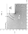
- the excess interstitial concentration and, hence, the boron diffusivity increase and the boron distribution broadens.
- the minimum in the peak net p-type concentration of the buried layer occurs at mid-width and is accentuated by the compensation of boron by the n-well doping.
- the gradient in the excess interstitial concentration drives the boron towards the trench edge.
- segregation induced boron depletion and n-type dopant pile-up reduce the net p-type concentration.
- Modeling shows that the peak net p-type concentration in the "boron puddle" is approximately 32% greater than at mid-width, for a 2 ⁇ m wide device. As the device width is reduced down to approximately 0.4 ⁇ m, the peak net p-type concentration increases because of decreased interstitial concentration at the top surface resulting from recombination on the trench sidewall.
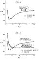
- Figure 3 shows measured V t versus W (width) characteristics compared with simulated results. As illustrated in Figure 3, the magnitude of V t drops by approximately 150 mV when the device width is reduced from 2 ⁇ m to 0.4 ⁇ m. This results in a loss of overdrive of approximately 100mV for the widest channel p-FETS used in a design.
- part of the present process for making trench-bounded buried-channel p-MOSFETS comprising the following steps: (1) implanting at least one deep phosphorus n-well; (2) implanting a boron buried-channel; and (3) initiating a 850°C dry gate oxidation step--results in an anomalous narrow channel behavior.
- the anomalous narrow channel behavior can be achieved by implementing a low temperature annealing step, utilizing an inert gas, immediately following the deep phosphorus implant and prior to the boron buried-channel implant.
- the low temperature annealing step may be initiated after the boron buried-channel implant and prior to the 850°C dry gate oxidation step.
- the low temperature anneal may be performed at a temperature of between about 750°C to about 800°C. Temperatures much above 800°C are undesirable as this will increase phosphorous diffusion. Temperatures much below 750°C result in reduced interstitial recombination. Regarding the duration of the annealing step, a reduction of the anomalous narrow channel behavior has been observed for periods ranging from about 10 minutes to about 120 minutes.
- the low temperature anneal is carried out with an inert gas, such as, by way of example and not by limitation, nitrogen or argon.
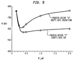
- FIG. 4 compares the simulated and measured V t vs. W characteristics for devices fabricated using recipe "B” with simulated behavior using recipe "A". As shown in Figure 4, the threshold voltage V t remains nearly constant as the device width is reduced from about 2 ⁇ m to about 0.4 ⁇ m. Specifically, the net p-type concentration peaks only 3% above mid-width value for a device width of 2 ⁇ m. The normal narrow channel behavior--increased magnitude of V t with decreasing W--is observed at device widths below about 0.4 ⁇ m.
- RTO rapid thermal oxidation
- A 850°C gate oxidation step
- process recipe C is carried out at temperatures ranging from about 1025°C to about 1075°C.
- the duration of the RTO gate oxidation step is dependent upon the desired thickness of the gate oxide. For example, for a gate oxide thickness of 80 angstroms, the duration of the RTO gate oxidation step would be about 1.3 minutes.
- the two can be used in conjunction, with the duration of the RTO step being reduced somewhat to be followed by the 850°C gate oxidation step.
Landscapes
- Engineering & Computer Science (AREA)
- Manufacturing & Machinery (AREA)
- Insulated Gate Type Field-Effect Transistor (AREA)
- Semiconductor Memories (AREA)
Applications Claiming Priority (2)
| Application Number | Priority Date | Filing Date | Title |
|---|---|---|---|
| US351924 | 1989-05-15 | ||
| US35192494A | 1994-12-08 | 1994-12-08 |
Publications (2)
| Publication Number | Publication Date |
|---|---|
| EP0720218A2 true EP0720218A2 (de) | 1996-07-03 |
| EP0720218A3 EP0720218A3 (de) | 1998-12-16 |
Family
ID=23383008
Family Applications (1)
| Application Number | Title | Priority Date | Filing Date |
|---|---|---|---|
| EP95119309A Ceased EP0720218A3 (de) | 1994-12-08 | 1995-12-07 | Verfahren zur Reduzierung des anormalen schmalen Kanaleffektes in p-MOSFETs mit einem durch einen Graben begrenzten begrabenem Kanal |
Country Status (4)
| Country | Link |
|---|---|
| EP (1) | EP0720218A3 (de) |
| JP (1) | JPH08241986A (de) |
| KR (1) | KR100359523B1 (de) |
| TW (1) | TW281800B (de) |
Cited By (2)
| Publication number | Priority date | Publication date | Assignee | Title |
|---|---|---|---|---|
| EP0889517A1 (de) * | 1997-06-30 | 1999-01-07 | Siemens Aktiengesellschaft | Integrierte CMOS-Schaltungen mit reduzierten Substratdefekten |
| EP1104936A1 (de) * | 1999-11-25 | 2001-06-06 | Mitsubishi Denki Kabushiki Kaisha | Herstellungsverfahren für ein Halbleiter-Bauelement, und dadurch hergestelltes Halbleiter-Bauelement |
Families Citing this family (2)
| Publication number | Priority date | Publication date | Assignee | Title |
|---|---|---|---|---|
| KR100468695B1 (ko) * | 1997-10-31 | 2005-03-16 | 삼성전자주식회사 | 짧은채널효과를개선시키기위한채널도우핑프로파일을갖는고성능모스트랜지스터제조방법 |
| KR100764439B1 (ko) * | 2006-04-25 | 2007-10-05 | 주식회사 하이닉스반도체 | 반도체 소자의 형성 방법 |
Family Cites Families (4)
| Publication number | Priority date | Publication date | Assignee | Title |
|---|---|---|---|---|
| KR940003218B1 (ko) * | 1988-03-24 | 1994-04-16 | 세이꼬 엡슨 가부시끼가이샤 | 반도체 장치 및 그 제조방법 |
| JPH02137263A (ja) * | 1988-11-17 | 1990-05-25 | Sanyo Electric Co Ltd | 半導体メモリ装置 |
| JPH04196488A (ja) * | 1990-11-28 | 1992-07-16 | Seiko Epson Corp | 半導体装置の製造方法 |
| US5559050A (en) * | 1994-06-30 | 1996-09-24 | International Business Machines Corporation | P-MOSFETS with enhanced anomalous narrow channel effect |
-
1995
- 1995-12-06 JP JP7317997A patent/JPH08241986A/ja not_active Withdrawn
- 1995-12-06 TW TW084112984A patent/TW281800B/zh not_active IP Right Cessation
- 1995-12-07 EP EP95119309A patent/EP0720218A3/de not_active Ceased
- 1995-12-08 KR KR1019950047670A patent/KR100359523B1/ko not_active Expired - Fee Related
Non-Patent Citations (3)
| Title |
|---|
| EL-KAREH B. ET AL: "Comparison of rapid thermal processing and furnace processing for quarter-micron CMOS", PROCEEDINGS OF THE SPIE, THE INTERNATIONAL SOCIETY FOR OPTICAL ENGINEERING, USA, vol. 2091, 27 September 1993 (1993-09-27) - 29 September 1993 (1993-09-29), MONTEREY, CA, pages 36 - 50, XP001001124, DOI: doi:10.1117/12.167352 * |
| OHE K. ET AL: "Narrow-Width Effects of shallow Trench-Isolated CMOS with n+Polysilicon Gate", IEEE TRANSACTIONS ON ELECTRON DEVICES, vol. 36, no. 6, June 1989 (1989-06-01), NEW YORK, US, pages 1110 - 1116, XP000003453, DOI: doi:10.1109/16.24355 * |
| SOLMI S. ET AL: "Effect of the annealing conditions on the electrical characteristic of p+/n shallow junctions", IEEE ELECTRON DEVICES LETTERS, vol. EDL-5, no. 9, September 1984 (1984-09-01), NEW YORK, US, pages 359 - 361, XP000821844 * |
Cited By (4)
| Publication number | Priority date | Publication date | Assignee | Title |
|---|---|---|---|---|
| EP0889517A1 (de) * | 1997-06-30 | 1999-01-07 | Siemens Aktiengesellschaft | Integrierte CMOS-Schaltungen mit reduzierten Substratdefekten |
| US5937288A (en) * | 1997-06-30 | 1999-08-10 | Siemens Aktiengesellschaft | CMOS integrated circuits with reduced substrate defects |
| EP1104936A1 (de) * | 1999-11-25 | 2001-06-06 | Mitsubishi Denki Kabushiki Kaisha | Herstellungsverfahren für ein Halbleiter-Bauelement, und dadurch hergestelltes Halbleiter-Bauelement |
| US6683004B1 (en) | 1999-11-25 | 2004-01-27 | Mitsubishi Denki Kabushiki Kaisha | Method of manufacturing a semiconductor device, and semiconductor device manufactured thereby |
Also Published As
| Publication number | Publication date |
|---|---|
| TW281800B (de) | 1996-07-21 |
| JPH08241986A (ja) | 1996-09-17 |
| KR100359523B1 (ko) | 2003-04-03 |
| KR960026784A (ko) | 1996-07-22 |
| EP0720218A3 (de) | 1998-12-16 |
Similar Documents
| Publication | Publication Date | Title |
|---|---|---|
| US5783469A (en) | Method for making nitrogenated gate structure for improved transistor performance | |
| US6228694B1 (en) | Method of increasing the mobility of MOS transistors by use of localized stress regions | |
| US7071067B1 (en) | Fabrication of integrated devices using nitrogen implantation | |
| US5552332A (en) | Process for fabricating a MOSFET device having reduced reverse short channel effects | |
| US6362082B1 (en) | Methodology for control of short channel effects in MOS transistors | |
| US5726459A (en) | GE-SI SOI MOS transistor and method of fabricating same | |
| KR100283712B1 (ko) | 반도체 장치의 제조 방법 | |
| US6255693B1 (en) | Ion implantation with programmable energy, angle, and beam current | |
| US4839301A (en) | Blanket CMOS channel stop implant employing a combination of n-channel and p-channel punch-through implants | |
| US5559050A (en) | P-MOSFETS with enhanced anomalous narrow channel effect | |
| US4851360A (en) | NMOS source/drain doping with both P and As | |
| US6080630A (en) | Method for forming a MOS device with self-compensating VT -implants | |
| US5858825A (en) | Methods for reducing anomalous narrow channel effect in trench-bounded buried-channel p-MOSFETS | |
| US5731637A (en) | Semiconductor device | |
| US6709961B2 (en) | Method for fabricating semiconductor device | |
| EP0720218A2 (de) | Verfahren zur Reduzierung des anormalen schmalen Kanaleffektes in p-MOSFETs mit einem durch einen Graben begrenzten begrabenem Kanal | |
| US4987088A (en) | Fabrication of CMOS devices with reduced gate length | |
| KR19990006812A (ko) | Mis 트랜지스터의 제조방법 | |
| US6974982B2 (en) | Method of manufacturing semiconductor device and semiconductor device | |
| HK1003958A (en) | Methods for reducing anomalous narrow channel effect in trench-bounded buried-channel p-mosfets | |
| Mandelman et al. | Anomalous narrow channel effect in trench-isolated buried-channel p-MOSFET's | |
| Pfiester et al. | Improved CMOS field isolation using germanium/boron implantation | |
| EP0806794A2 (de) | Verfahren zur Bildung von flachen dotierten Gebieten in einem Halbleitersubstrat, mittels Voramorphisierung und Ionen-Implantation | |
| US6423601B1 (en) | Retrograde well structure formation by nitrogen implantation | |
| US6767808B2 (en) | Method for fabricating semiconductor device |
Legal Events
| Date | Code | Title | Description |
|---|---|---|---|
| PUAI | Public reference made under article 153(3) epc to a published international application that has entered the european phase |
Free format text: ORIGINAL CODE: 0009012 |
|
| AK | Designated contracting states |
Kind code of ref document: A2 Designated state(s): AT DE FR GB IE IT NL |
|
| PUAL | Search report despatched |
Free format text: ORIGINAL CODE: 0009013 |
|
| AK | Designated contracting states |
Kind code of ref document: A3 Designated state(s): AT DE FR GB IE IT NL |
|
| 17P | Request for examination filed |
Effective date: 19990205 |
|
| 17Q | First examination report despatched |
Effective date: 20010601 |
|
| RAP1 | Party data changed (applicant data changed or rights of an application transferred) |
Owner name: INTERNATIONAL BUSINESS MACHINES CORPORATION Owner name: INFINEON TECHNOLOGIES AG |
|
| GRAG | Despatch of communication of intention to grant |
Free format text: ORIGINAL CODE: EPIDOS AGRA |
|
| STAA | Information on the status of an ep patent application or granted ep patent |
Free format text: STATUS: THE APPLICATION HAS BEEN REFUSED |
|
| 18R | Application refused |
Effective date: 20021025 |
|
| REG | Reference to a national code |
Ref country code: HK Ref legal event code: WD Ref document number: 1003958 Country of ref document: HK |