EP0720218A2 - Methods for reducing anomalous narrow channel effect in trench-bounded buried-channel p-MOSFETS - Google Patents
Methods for reducing anomalous narrow channel effect in trench-bounded buried-channel p-MOSFETS Download PDFInfo
- Publication number
- EP0720218A2 EP0720218A2 EP95119309A EP95119309A EP0720218A2 EP 0720218 A2 EP0720218 A2 EP 0720218A2 EP 95119309 A EP95119309 A EP 95119309A EP 95119309 A EP95119309 A EP 95119309A EP 0720218 A2 EP0720218 A2 EP 0720218A2
- Authority
- EP
- European Patent Office
- Prior art keywords
- channel
- buried
- gate oxidation
- boron
- trench
- Prior art date
- Legal status (The legal status is an assumption and is not a legal conclusion. Google has not performed a legal analysis and makes no representation as to the accuracy of the status listed.)
- Ceased
Links
Images

Classifications
-
- H—ELECTRICITY
- H10—SEMICONDUCTOR DEVICES; ELECTRIC SOLID-STATE DEVICES NOT OTHERWISE PROVIDED FOR
- H10B—ELECTRONIC MEMORY DEVICES
- H10B12/00—Dynamic random access memory [DRAM] devices
- H10B12/01—Manufacture or treatment
- H10B12/02—Manufacture or treatment for one transistor one-capacitor [1T-1C] memory cells
- H10B12/05—Making the transistor
-
- H—ELECTRICITY
- H10—SEMICONDUCTOR DEVICES; ELECTRIC SOLID-STATE DEVICES NOT OTHERWISE PROVIDED FOR
- H10D—INORGANIC ELECTRIC SEMICONDUCTOR DEVICES
- H10D84/00—Integrated devices formed in or on semiconductor substrates that comprise only semiconducting layers, e.g. on Si wafers or on GaAs-on-Si wafers
- H10D84/01—Manufacture or treatment
- H10D84/0123—Integrating together multiple components covered by H10D12/00 or H10D30/00, e.g. integrating multiple IGBTs
- H10D84/0126—Integrating together multiple components covered by H10D12/00 or H10D30/00, e.g. integrating multiple IGBTs the components including insulated gates, e.g. IGFETs
- H10D84/0128—Manufacturing their channels
-
- H—ELECTRICITY
- H10—SEMICONDUCTOR DEVICES; ELECTRIC SOLID-STATE DEVICES NOT OTHERWISE PROVIDED FOR
- H10D—INORGANIC ELECTRIC SEMICONDUCTOR DEVICES
- H10D30/00—Field-effect transistors [FET]
- H10D30/60—Insulated-gate field-effect transistors [IGFET]
- H10D30/637—Lateral IGFETs having no inversion channels, e.g. buried channel lateral IGFETs, normally-on lateral IGFETs or depletion-mode lateral IGFETs
-
- H—ELECTRICITY
- H10—SEMICONDUCTOR DEVICES; ELECTRIC SOLID-STATE DEVICES NOT OTHERWISE PROVIDED FOR
- H10D—INORGANIC ELECTRIC SEMICONDUCTOR DEVICES
- H10D84/00—Integrated devices formed in or on semiconductor substrates that comprise only semiconducting layers, e.g. on Si wafers or on GaAs-on-Si wafers
- H10D84/01—Manufacture or treatment
- H10D84/02—Manufacture or treatment characterised by using material-based technologies
- H10D84/03—Manufacture or treatment characterised by using material-based technologies using Group IV technology, e.g. silicon technology or silicon-carbide [SiC] technology
- H10D84/038—Manufacture or treatment characterised by using material-based technologies using Group IV technology, e.g. silicon technology or silicon-carbide [SiC] technology using silicon technology, e.g. SiGe
Definitions
- the present invention generally relates to methods of manufacture of trench-bounded buried-channel p-type metal oxide semiconductor field effect transistors (p-MOSFETs) as used in dynamic random access memory (DRAM) technologies and, more particularly, to methods for significantly reducing the anomalous buried-channel p-MOSFET sensitivity to device width.
- p-MOSFETs trench-bounded buried-channel p-type metal oxide semiconductor field effect transistors
- DRAM dynamic random access memory
- V t threshold voltage
- W des and L des are the design width and design length of the device, respectively.
- the performance of the widest devices is compromised as a result of the higher than desired V t . Consequently, to assure that the narrowest devices meet the off-current objective, the magnitude of the V t of the widest devices must be set higher than required by the off-current objective. This results in a performance penalty for the wider devices of typically a 100mV loss of overdrive.
- a method for eliminating the anomalous channel effect including the steps of implanting at least one deep phosphorous n-well; initiating a low temperature anneal using an inert gas; implanting a boron buried-channel; and initiating a gate oxidation.
- the low temperature annealing step is performed at about 750°C to about 800°C, for a period of about 10 minutes to about 120 minutes, and utilizes an inert gas, such as, for example, nitrogen or argon.
- the low temperature anneal may be performed after implanting the boron buried-channel and prior to initiating the gate oxidation.
- a method for eliminating the anomalous channel effect including the steps of implanting at least one deep phosphorous n-well; implanting a boron buried-channel; and initiating a rapid thermal oxidation (RTO) gate oxidation step.
- the RTO is performed at about 1025°C to about 1075°C for a period of time sufficient to grow the gate oxide.
- the RTO step may be followed by a standard gate oxidation step performed at about 850°C.
- the excess interstitial concentration and, hence, the boron diffusivity increase and the boron distribution broadens.
- the minimum in the peak net p-type concentration of the buried layer occurs at mid-width and is accentuated by the compensation of boron by the n-well doping.
- the gradient in the excess interstitial concentration drives the boron towards the trench edge.
- segregation induced boron depletion and n-type dopant pile-up reduce the net p-type concentration.
- Modeling shows that the peak net p-type concentration in the "boron puddle" is approximately 32% greater than at mid-width, for a 2 ⁇ m wide device. As the device width is reduced down to approximately 0.4 ⁇ m, the peak net p-type concentration increases because of decreased interstitial concentration at the top surface resulting from recombination on the trench sidewall.
- Figure 3 shows measured V t versus W (width) characteristics compared with simulated results. As illustrated in Figure 3, the magnitude of V t drops by approximately 150 mV when the device width is reduced from 2 ⁇ m to 0.4 ⁇ m. This results in a loss of overdrive of approximately 100mV for the widest channel p-FETS used in a design.
- part of the present process for making trench-bounded buried-channel p-MOSFETS comprising the following steps: (1) implanting at least one deep phosphorus n-well; (2) implanting a boron buried-channel; and (3) initiating a 850°C dry gate oxidation step--results in an anomalous narrow channel behavior.
- the anomalous narrow channel behavior can be achieved by implementing a low temperature annealing step, utilizing an inert gas, immediately following the deep phosphorus implant and prior to the boron buried-channel implant.
- the low temperature annealing step may be initiated after the boron buried-channel implant and prior to the 850°C dry gate oxidation step.
- the low temperature anneal may be performed at a temperature of between about 750°C to about 800°C. Temperatures much above 800°C are undesirable as this will increase phosphorous diffusion. Temperatures much below 750°C result in reduced interstitial recombination. Regarding the duration of the annealing step, a reduction of the anomalous narrow channel behavior has been observed for periods ranging from about 10 minutes to about 120 minutes.
- the low temperature anneal is carried out with an inert gas, such as, by way of example and not by limitation, nitrogen or argon.
- FIG. 4 compares the simulated and measured V t vs. W characteristics for devices fabricated using recipe "B” with simulated behavior using recipe "A". As shown in Figure 4, the threshold voltage V t remains nearly constant as the device width is reduced from about 2 ⁇ m to about 0.4 ⁇ m. Specifically, the net p-type concentration peaks only 3% above mid-width value for a device width of 2 ⁇ m. The normal narrow channel behavior--increased magnitude of V t with decreasing W--is observed at device widths below about 0.4 ⁇ m.
- RTO rapid thermal oxidation
- A 850°C gate oxidation step
- process recipe C is carried out at temperatures ranging from about 1025°C to about 1075°C.
- the duration of the RTO gate oxidation step is dependent upon the desired thickness of the gate oxide. For example, for a gate oxide thickness of 80 angstroms, the duration of the RTO gate oxidation step would be about 1.3 minutes.
- the two can be used in conjunction, with the duration of the RTO step being reduced somewhat to be followed by the 850°C gate oxidation step.
Landscapes
- Engineering & Computer Science (AREA)
- Manufacturing & Machinery (AREA)
- Insulated Gate Type Field-Effect Transistor (AREA)
- Semiconductor Memories (AREA)
Abstract
Description
- The present invention generally relates to methods of manufacture of trench-bounded buried-channel p-type metal oxide semiconductor field effect transistors (p-MOSFETs) as used in dynamic random access memory (DRAM) technologies and, more particularly, to methods for significantly reducing the anomalous buried-channel p-MOSFET sensitivity to device width.
- Corner conduction in trench isolated n-channel MOSFETs, as reported by A. Bryant, W. Haensch, S. Geissler, J. Mandelman, D. Poindexter, and M. Steger in "The Current-Carrying Corner Inherent to Trench Isolation", IEEE Electron Device Letters, vol. 14, no. 8, pp. 412-414 (1993), and B. Davari, C. Koburger, T. Furukawa, Y. Taur, W. Noble, J. Warnock, and J. Mauer in "A Variable-Size Shallow Trench Isolation (STI) Technology with Diffused Sidewall Doping for Submicron CMOS", 1988 IEDM Technical Digest, pp. 92-95 (1988), could be a significant contributor to standby current in low standby power ultra large scale integration (ULSI) applications. A manifestation of corner conduction is inverse narrow channel effect when the standard current definition of threshold voltage, Vt,

- However, corner conduction in buried-channel p-MOSFETs has not, heretofore, been recognized as a concern. In buried-channel p-MOSFETs, the polarity of the work function difference between the N+ poly gate and the buried p-layer depletes the buried layer of carriers at low gate voltages. Due to the geometrically enhanced field at the silicon corner, it is expected that, when doping is uniform across the device width, the magnitude of Vt at the corners of these devices is greater than at mid-channel. This leads to a normal channel effect, wherein the magnitude of Vt increases with decreasing width of the device.
- An anomalous (or inverse) narrow channel behavior has been observed in trench-bounded buried-channel p-MOSFETs (as used in contemporary DRAM technologies). Specifically, it has been observed that the magnitude of the threshold voltage, Vt, drops by approximately 100mV when going from a device width of 20µm down to 2µm. The magnitude of Vt drops more rapidly with further width reduction to approximately 0.4µm. For devices narrower than 0.4µm, the expected normal narrow channel effect is observed, that is, the magnitude of Vt increases with decreasing width of the device.
- If the buried-channel boron dose is decreased to assure that the off-current is less than or equal to the objective over the entire range of design widths, the performance of the widest devices is compromised as a result of the higher than desired Vt. Consequently, to assure that the narrowest devices meet the off-current objective, the magnitude of the Vt of the widest devices must be set higher than required by the off-current objective. This results in a performance penalty for the wider devices of typically a 100mV loss of overdrive.
- It is therefore an object of the present invention to provide a method of minimizing the anomalous channel effect and resulting sensitivity to device width.
- To achieve these and other advantages and in accordance with the purpose of the invention embodied and broadly described herein, in one embodiment of the invention, there is provided a method for eliminating the anomalous channel effect including the steps of implanting at least one deep phosphorous n-well; initiating a low temperature anneal using an inert gas; implanting a boron buried-channel; and initiating a gate oxidation. The low temperature annealing step is performed at about 750°C to about 800°C, for a period of about 10 minutes to about 120 minutes, and utilizes an inert gas, such as, for example, nitrogen or argon. Alternatively, the low temperature anneal may be performed after implanting the boron buried-channel and prior to initiating the gate oxidation.
- In another aspect of the invention, there is provided a method for eliminating the anomalous channel effect including the steps of implanting at least one deep phosphorous n-well; implanting a boron buried-channel; and initiating a rapid thermal oxidation (RTO) gate oxidation step. The RTO is performed at about 1025°C to about 1075°C for a period of time sufficient to grow the gate oxide. In still another aspect of the invention, the RTO step may be followed by a standard gate oxidation step performed at about 850°C.
- It is to be understood that both the foregoing general description and the following detailed description are exemplary and explanatory and are intended to provide further explanation of the invention as claimed.
- The foregoing and other objects, aspects and advantages will be better understood from the following detailed description of the embodiments of the invention with reference to the drawings, in which:
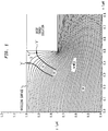
- Figure 1 is a graph superimposed on a cross-section of a portion of an oxide trench isolation showing interstitial (excess) contours at the beginning of an 850°C gate oxidation step using process recipe "A";
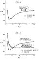
- Figure 2 is a cross-section similar to Figure 1 showing the boron buried layer puddle responsible for anomalous Vt dependence on channel width using process recipe "A";
- Figure 3 is a graph showing measured and modeled Vt versus width (W) for process recipe "A" demonstrating the anomalous Vt dependence on width down to ≈0.4µm;
- Figure 4 is a graph showing the effect on the anomalous narrow channel behavior of the solution using process recipe "B" according to the invention; and
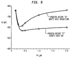
- Figure 5 is a graph showing the effect on the anomalous narrow channel behavior of the solution using process recipe "C" according to the invention.
- In a standard 0.25µm CMOS process, a 15 minute, 850°C dry gate oxidation step immediately follows the n-well and boron buried-channel implants (referred to as process recipe "A"). As a result of damage from the deep phosphorous n-well implant (2.5×1013cm-2, 500keV) used for latchup suppression, a high concentration source of excess interstitials is created approximately 0.8µm beneath the silicon surface. Since the trench sidewall and top surface of the device are efficient sinks for excess interstitials, an interstitial gradient, shown in Figure 1, is established. Heavy arrows 'a' and 'b' depict the direction of the interstitial flux.
- The interstitial gradient towards the interfaces, driven by implant induced damage, is created despite interstitial injection at the oxidizing top surface. Under intrinsic diffusion conditions, the dependence of the boron flux on the excess interstitial concentration can be approximated as

where DB is the boron diffusivity, and
- Moving along the peak of the boron buried-layer (approximately 30nm deep) from trench edge towards mid-width, the excess interstitial concentration and, hence, the boron diffusivity, increase and the boron distribution broadens. The minimum in the peak net p-type concentration of the buried layer occurs at mid-width and is accentuated by the compensation of boron by the n-well doping. Furthermore, the gradient in the excess interstitial concentration drives the boron towards the trench edge. Within approximately 30nm of the trench edge, segregation induced boron depletion and n-type dopant pile-up reduce the net p-type concentration. The overall effect of the excess interstitial distribution on the diffusion of boron during the 850°C gate oxidation step is the creation of a "boron puddle" 100 near the trench edge, as shown by the simulated net doping distribution at the end of the process in Figure 2.
- Modeling shows that the peak net p-type concentration in the "boron puddle" is approximately 32% greater than at mid-width, for a 2µm wide device. As the device width is reduced down to approximately 0.4µm, the peak net p-type concentration increases because of decreased interstitial concentration at the top surface resulting from recombination on the trench sidewall.
- For still narrower devices, the effect of the n-type dopant pileup on the trench sidewall reduces the buried layer concentration. Figure 3 shows measured Vt versus W (width) characteristics compared with simulated results. As illustrated in Figure 3, the magnitude of Vt drops by approximately 150 mV when the device width is reduced from 2µm to 0.4µm. This results in a loss of overdrive of approximately 100mV for the widest channel p-FETS used in a design.
- It is noteworthy that evidence of a comparable boron puddle for the n-MOSFET is neither observed experimentally nor predicted by modeling. As calculated using the implant damage model of G. Hobler and S. Selberherr in "Two-Dimensional Modeling of Ion Implantation Induced Point Defects", IEEE Trans. Computer-Aided Design, vol. 7, no. 2, pp. 174-181 (1988), damage from the deep boron implant (2.0×1013cm-2, 260keV) used for latchup suppression in the n-MOSFET is significantly less than damage caused by the phosphorus implant in the p-MOSFET.
- As noted above, part of the present process for making trench-bounded buried-channel p-MOSFETS (recipe "A")--comprising the following steps: (1) implanting at least one deep phosphorus n-well; (2) implanting a boron buried-channel; and (3) initiating a 850°C dry gate oxidation step--results in an anomalous narrow channel behavior.
- It has been demonstrated that reduction of the anomalous narrow channel behavior can be achieved by implementing a low temperature annealing step, utilizing an inert gas, immediately following the deep phosphorus implant and prior to the boron buried-channel implant. Alternatively, the low temperature annealing step may be initiated after the boron buried-channel implant and prior to the 850°C dry gate oxidation step.
- The low temperature anneal may be performed at a temperature of between about 750°C to about 800°C. Temperatures much above 800°C are undesirable as this will increase phosphorous diffusion. Temperatures much below 750°C result in reduced interstitial recombination. Regarding the duration of the annealing step, a reduction of the anomalous narrow channel behavior has been observed for periods ranging from about 10 minutes to about 120 minutes. The low temperature anneal is carried out with an inert gas, such as, by way of example and not by limitation, nitrogen or argon.
- This annealing process results in rapid excess interstitial recombination on the Si/SiO2 interfaces; thus the transient enhanced diffusion (TED) of boron is greatly reduced during the subsequent 850°C gate oxidation. Figure 4 compares the simulated and measured Vt vs. W characteristics for devices fabricated using recipe "B" with simulated behavior using recipe "A". As shown in Figure 4, the threshold voltage Vt remains nearly constant as the device width is reduced from about 2µm to about 0.4µm. Specifically, the net p-type concentration peaks only 3% above mid-width value for a device width of 2µm. The normal narrow channel behavior--increased magnitude of Vt with decreasing W--is observed at device widths below about 0.4µm.
- Although the addition of this low temperature inert gas annealing step results in a drastically reduced "boron puddle" it also results in a lower magnitude of wide device Vt, since the reduced transient enhanced diffusion (TED) of boron leaves a higher peak net p-type concentration in the buried layer.
- In another embodiment of the invention, it has also been demonstrated that reduction of the anomalous narrow channel behavior can be achieved by substituting a rapid thermal oxidation (RTO) step for the 850°C gate oxidation step (recipe "A") following the deep phosphorous implant. The RTO gate oxidation step (referred to as process recipe "C") is carried out at temperatures ranging from about 1025°C to about 1075°C. The duration of the RTO gate oxidation step is dependent upon the desired thickness of the gate oxide. For example, for a gate oxide thickness of 80 angstroms, the duration of the RTO gate oxidation step would be about 1.3 minutes.
- Alternatively, rather the substitute the RTO gate oxidation step for the 850°C gate oxidation step, the two can be used in conjunction, with the duration of the RTO step being reduced somewhat to be followed by the 850°C gate oxidation step.
- During the RTO gate oxidation step, transient enhanced diffusion (TED) of boron is negligible, since the excess interstitial concentration is reduced at the elevated temperature. Figure 5 compares the simulated Vt vs. W characteristics for devices fabricated using recipe "C" with simulated behavior using recipe "A". As shown in Figure 5, the threshold voltage Vt remains nearly constant as the device width is reduced from about 2µm to about 0.4µm. The normal narrow channel behavior is observed at device widths below about 0.4µm. Simulation shows the magnitude of the "boron puddle" and the anomalous Vt width dependence are negligible for this process.
- While the invention has been described in terms of the above embodiments, those skilled in the art will recognize that the invention can be practiced with modification within the spirit and scope of the appended claims.
Claims (7)
- Having thus described my invention, what I claim as new and desire to secure by Letters Patent is as follows:
- A method for reducing an anomalous narrow channel effect in trench-bounded buried-channel p-MOSFETS, the method comprising the steps of:
implanting at least one deep phosphorous n-well;
performing one of initiating a low temperature anneal using an inert gas or implanting a boron buried-channel;
performing the other of initiating a low temperature anneal using an inert gas or implanting a boron buried-channel; and
initiating a dry gate oxidation. - The method recited in claim 1, wherein the annealing step is performed between a temperature of about 750°C to about 800°C, for a period of about 10 minutes to about 120 minutes, and the inert gas is nitrogen or argon.
- The method recited in claim 1, wherein the dry gate oxidation is performed at a temperature of about 850°C.
- A method for reducing an anomalous narrow channel effect in trench-bounded buried-channel p-MOSFETS, the method comprising the steps of:
implanting a deep phosphorous n-well;
implanting a boron buried-channel; and
initiating a rapid thermal oxidation (RTO) gate oxidation. - The method recited in claim 4, wherein the rapid thermal oxidation step is performed at between about 1025°C to about 1075°C for a period of time sufficient to grow a desired gate oxide thickness.
- The method recited in claim 4, further including an 850°C gate oxidation step following the RTO gate oxidation step.
Applications Claiming Priority (2)
| Application Number | Priority Date | Filing Date | Title |
|---|---|---|---|
| US35192494A | 1994-12-08 | 1994-12-08 | |
| US351924 | 1994-12-08 |
Publications (2)
| Publication Number | Publication Date |
|---|---|
| EP0720218A2 true EP0720218A2 (en) | 1996-07-03 |
| EP0720218A3 EP0720218A3 (en) | 1998-12-16 |
Family
ID=23383008
Family Applications (1)
| Application Number | Title | Priority Date | Filing Date |
|---|---|---|---|
| EP95119309A Ceased EP0720218A3 (en) | 1994-12-08 | 1995-12-07 | Methods for reducing anomalous narrow channel effect in trench-bounded buried-channel p-MOSFETS |
Country Status (4)
| Country | Link |
|---|---|
| EP (1) | EP0720218A3 (en) |
| JP (1) | JPH08241986A (en) |
| KR (1) | KR100359523B1 (en) |
| TW (1) | TW281800B (en) |
Cited By (2)
| Publication number | Priority date | Publication date | Assignee | Title |
|---|---|---|---|---|
| EP0889517A1 (en) * | 1997-06-30 | 1999-01-07 | Siemens Aktiengesellschaft | CMOS Integrated circuits with reduced substrate defects |
| EP1104936A1 (en) * | 1999-11-25 | 2001-06-06 | Mitsubishi Denki Kabushiki Kaisha | Method of manufacturing a semiconductor device, and semiconductor device manufactured thereby |
Families Citing this family (2)
| Publication number | Priority date | Publication date | Assignee | Title |
|---|---|---|---|---|
| KR100468695B1 (en) * | 1997-10-31 | 2005-03-16 | 삼성전자주식회사 | Method for fabricting high performance MOS transistor having channel doping profile to improve short channel effect |
| KR100764439B1 (en) * | 2006-04-25 | 2007-10-05 | 주식회사 하이닉스반도체 | Method of forming a semiconductor device |
Family Cites Families (4)
| Publication number | Priority date | Publication date | Assignee | Title |
|---|---|---|---|---|
| KR940003218B1 (en) * | 1988-03-24 | 1994-04-16 | 세이꼬 엡슨 가부시끼가이샤 | Semiconductor device and manufacturing method thereof |
| JPH02137263A (en) * | 1988-11-17 | 1990-05-25 | Sanyo Electric Co Ltd | Semiconductor memory device |
| JPH04196488A (en) * | 1990-11-28 | 1992-07-16 | Seiko Epson Corp | Manufacturing method of semiconductor device |
| US5559050A (en) * | 1994-06-30 | 1996-09-24 | International Business Machines Corporation | P-MOSFETS with enhanced anomalous narrow channel effect |
-
1995
- 1995-12-06 TW TW084112984A patent/TW281800B/zh not_active IP Right Cessation
- 1995-12-06 JP JP7317997A patent/JPH08241986A/en not_active Withdrawn
- 1995-12-07 EP EP95119309A patent/EP0720218A3/en not_active Ceased
- 1995-12-08 KR KR1019950047670A patent/KR100359523B1/en not_active Expired - Fee Related
Non-Patent Citations (3)
| Title |
|---|
| EL-KAREH B. ET AL: "Comparison of rapid thermal processing and furnace processing for quarter-micron CMOS", PROCEEDINGS OF THE SPIE, THE INTERNATIONAL SOCIETY FOR OPTICAL ENGINEERING, USA, vol. 2091, 27 September 1993 (1993-09-27) - 29 September 1993 (1993-09-29), MONTEREY, CA, pages 36 - 50, XP001001124, DOI: doi:10.1117/12.167352 * |
| OHE K. ET AL: "Narrow-Width Effects of shallow Trench-Isolated CMOS with n+Polysilicon Gate", IEEE TRANSACTIONS ON ELECTRON DEVICES, vol. 36, no. 6, June 1989 (1989-06-01), NEW YORK, US, pages 1110 - 1116, XP000003453, DOI: doi:10.1109/16.24355 * |
| SOLMI S. ET AL: "Effect of the annealing conditions on the electrical characteristic of p+/n shallow junctions", IEEE ELECTRON DEVICES LETTERS, vol. EDL-5, no. 9, September 1984 (1984-09-01), NEW YORK, US, pages 359 - 361, XP000821844 * |
Cited By (4)
| Publication number | Priority date | Publication date | Assignee | Title |
|---|---|---|---|---|
| EP0889517A1 (en) * | 1997-06-30 | 1999-01-07 | Siemens Aktiengesellschaft | CMOS Integrated circuits with reduced substrate defects |
| US5937288A (en) * | 1997-06-30 | 1999-08-10 | Siemens Aktiengesellschaft | CMOS integrated circuits with reduced substrate defects |
| EP1104936A1 (en) * | 1999-11-25 | 2001-06-06 | Mitsubishi Denki Kabushiki Kaisha | Method of manufacturing a semiconductor device, and semiconductor device manufactured thereby |
| US6683004B1 (en) | 1999-11-25 | 2004-01-27 | Mitsubishi Denki Kabushiki Kaisha | Method of manufacturing a semiconductor device, and semiconductor device manufactured thereby |
Also Published As
| Publication number | Publication date |
|---|---|
| EP0720218A3 (en) | 1998-12-16 |
| JPH08241986A (en) | 1996-09-17 |
| KR100359523B1 (en) | 2003-04-03 |
| TW281800B (en) | 1996-07-21 |
| KR960026784A (en) | 1996-07-22 |
Similar Documents
| Publication | Publication Date | Title |
|---|---|---|
| US5783469A (en) | Method for making nitrogenated gate structure for improved transistor performance | |
| US6228694B1 (en) | Method of increasing the mobility of MOS transistors by use of localized stress regions | |
| US7071067B1 (en) | Fabrication of integrated devices using nitrogen implantation | |
| US5552332A (en) | Process for fabricating a MOSFET device having reduced reverse short channel effects | |
| US6362082B1 (en) | Methodology for control of short channel effects in MOS transistors | |
| US5359221A (en) | Semiconductor device | |
| US5726459A (en) | GE-SI SOI MOS transistor and method of fabricating same | |
| JP2697392B2 (en) | Method of manufacturing complementary semiconductor device | |
| KR100283712B1 (en) | Manufacturing Method of Semiconductor Device | |
| US6255693B1 (en) | Ion implantation with programmable energy, angle, and beam current | |
| US4839301A (en) | Blanket CMOS channel stop implant employing a combination of n-channel and p-channel punch-through implants | |
| US5559050A (en) | P-MOSFETS with enhanced anomalous narrow channel effect | |
| US4851360A (en) | NMOS source/drain doping with both P and As | |
| US6080630A (en) | Method for forming a MOS device with self-compensating VT -implants | |
| US5858825A (en) | Methods for reducing anomalous narrow channel effect in trench-bounded buried-channel p-MOSFETS | |
| US5731637A (en) | Semiconductor device | |
| US6709961B2 (en) | Method for fabricating semiconductor device | |
| EP0720218A2 (en) | Methods for reducing anomalous narrow channel effect in trench-bounded buried-channel p-MOSFETS | |
| US4987088A (en) | Fabrication of CMOS devices with reduced gate length | |
| KR19990006812A (en) | Method of manufacturing MIS transistor | |
| US6974982B2 (en) | Method of manufacturing semiconductor device and semiconductor device | |
| HK1003958A (en) | Methods for reducing anomalous narrow channel effect in trench-bounded buried-channel p-mosfets | |
| Mandelman et al. | Anomalous narrow channel effect in trench-isolated buried-channel p-MOSFET's | |
| Pfiester et al. | Improved CMOS field isolation using germanium/boron implantation | |
| EP0806794A2 (en) | Method of forming shallow doped regions in a semiconductor substrate, using preamorphization and ion implantation |
Legal Events
| Date | Code | Title | Description |
|---|---|---|---|
| PUAI | Public reference made under article 153(3) epc to a published international application that has entered the european phase |
Free format text: ORIGINAL CODE: 0009012 |
|
| AK | Designated contracting states |
Kind code of ref document: A2 Designated state(s): AT DE FR GB IE IT NL |
|
| PUAL | Search report despatched |
Free format text: ORIGINAL CODE: 0009013 |
|
| AK | Designated contracting states |
Kind code of ref document: A3 Designated state(s): AT DE FR GB IE IT NL |
|
| 17P | Request for examination filed |
Effective date: 19990205 |
|
| 17Q | First examination report despatched |
Effective date: 20010601 |
|
| RAP1 | Party data changed (applicant data changed or rights of an application transferred) |
Owner name: INTERNATIONAL BUSINESS MACHINES CORPORATION Owner name: INFINEON TECHNOLOGIES AG |
|
| GRAG | Despatch of communication of intention to grant |
Free format text: ORIGINAL CODE: EPIDOS AGRA |
|
| STAA | Information on the status of an ep patent application or granted ep patent |
Free format text: STATUS: THE APPLICATION HAS BEEN REFUSED |
|
| 18R | Application refused |
Effective date: 20021025 |
|
| REG | Reference to a national code |
Ref country code: HK Ref legal event code: WD Ref document number: 1003958 Country of ref document: HK |