EP0720154A2 - Electrode à couche mince pour tel qu'une tête à effet magnétorésistif et procédé de fabrication - Google Patents
Electrode à couche mince pour tel qu'une tête à effet magnétorésistif et procédé de fabrication Download PDFInfo
- Publication number
- EP0720154A2 EP0720154A2 EP95309423A EP95309423A EP0720154A2 EP 0720154 A2 EP0720154 A2 EP 0720154A2 EP 95309423 A EP95309423 A EP 95309423A EP 95309423 A EP95309423 A EP 95309423A EP 0720154 A2 EP0720154 A2 EP 0720154A2
- Authority
- EP
- European Patent Office
- Prior art keywords
- thin film
- electrode
- tantalum
- molybdenum
- molybdenum alloy
- Prior art date
- Legal status (The legal status is an assumption and is not a legal conclusion. Google has not performed a legal analysis and makes no representation as to the accuracy of the status listed.)
- Withdrawn
Links
Images


Classifications
-
- G—PHYSICS
- G11—INFORMATION STORAGE
- G11B—INFORMATION STORAGE BASED ON RELATIVE MOVEMENT BETWEEN RECORD CARRIER AND TRANSDUCER
- G11B5/00—Recording by magnetisation or demagnetisation of a record carrier; Reproducing by magnetic means; Record carriers therefor
- G11B5/127—Structure or manufacture of heads, e.g. inductive
- G11B5/33—Structure or manufacture of flux-sensitive heads, i.e. for reproduction only; Combination of such heads with means for recording or erasing only
- G11B5/39—Structure or manufacture of flux-sensitive heads, i.e. for reproduction only; Combination of such heads with means for recording or erasing only using magneto-resistive devices or effects
- G11B5/3903—Structure or manufacture of flux-sensitive heads, i.e. for reproduction only; Combination of such heads with means for recording or erasing only using magneto-resistive devices or effects using magnetic thin film layers or their effects, the films being part of integrated structures
-
- C—CHEMISTRY; METALLURGY
- C23—COATING METALLIC MATERIAL; COATING MATERIAL WITH METALLIC MATERIAL; CHEMICAL SURFACE TREATMENT; DIFFUSION TREATMENT OF METALLIC MATERIAL; COATING BY VACUUM EVAPORATION, BY SPUTTERING, BY ION IMPLANTATION OR BY CHEMICAL VAPOUR DEPOSITION, IN GENERAL; INHIBITING CORROSION OF METALLIC MATERIAL OR INCRUSTATION IN GENERAL
- C23C—COATING METALLIC MATERIAL; COATING MATERIAL WITH METALLIC MATERIAL; SURFACE TREATMENT OF METALLIC MATERIAL BY DIFFUSION INTO THE SURFACE, BY CHEMICAL CONVERSION OR SUBSTITUTION; COATING BY VACUUM EVAPORATION, BY SPUTTERING, BY ION IMPLANTATION OR BY CHEMICAL VAPOUR DEPOSITION, IN GENERAL
- C23C14/00—Coating by vacuum evaporation, by sputtering or by ion implantation of the coating forming material
- C23C14/06—Coating by vacuum evaporation, by sputtering or by ion implantation of the coating forming material characterised by the coating material
- C23C14/14—Metallic material, boron or silicon
- C23C14/18—Metallic material, boron or silicon on other inorganic substrates
- C23C14/185—Metallic material, boron or silicon on other inorganic substrates by cathodic sputtering
-
- G—PHYSICS
- G11—INFORMATION STORAGE
- G11B—INFORMATION STORAGE BASED ON RELATIVE MOVEMENT BETWEEN RECORD CARRIER AND TRANSDUCER
- G11B5/00—Recording by magnetisation or demagnetisation of a record carrier; Reproducing by magnetic means; Record carriers therefor
- G11B5/127—Structure or manufacture of heads, e.g. inductive
- G11B5/33—Structure or manufacture of flux-sensitive heads, i.e. for reproduction only; Combination of such heads with means for recording or erasing only
- G11B5/39—Structure or manufacture of flux-sensitive heads, i.e. for reproduction only; Combination of such heads with means for recording or erasing only using magneto-resistive devices or effects
- G11B5/3903—Structure or manufacture of flux-sensitive heads, i.e. for reproduction only; Combination of such heads with means for recording or erasing only using magneto-resistive devices or effects using magnetic thin film layers or their effects, the films being part of integrated structures
- G11B5/399—Structure or manufacture of flux-sensitive heads, i.e. for reproduction only; Combination of such heads with means for recording or erasing only using magneto-resistive devices or effects using magnetic thin film layers or their effects, the films being part of integrated structures with intrinsic biasing, e.g. provided by equipotential strips
Definitions
- the present invention relates to electrode thin films magnetoresistive effect heads and magnetoresistive effect heads having a function of reading data based on magnetoresistive effect, and method of manufacturing the same.
- Ta tantalum
- a thin film of tantalum which is formed through a sputtering process is usually ⁇ -tantalum having a teragonal crystal structure, and its resistivity is as high as 180 to 220 [ ⁇ cm] (as disclosed in, for instance, "Applied Physics Letters", Vol. 7, pp. 51-52, 1965).
- the thin film of tantalum nitride (TaN) in contrast is low in resistivity, but it has a demerit that its manufacture margin is very narrow (as shown in, for instance, Proceeding of IEEE, Vo.l. 52, pp. 1450-1462, 1964), making it difficult to obtain a thin film having stable characteristics.
- a tantalum-molybdenum alloy thin film which is obtainable by adding 15 atomic % or above of molybdenum to tantalum, has low resistivity and wide manufacture margin. Molybdenum, however, is readily subject to corrosion, and in the tantalum-molybdenum alloy thin film the corrosion resistance and etching solution resistance become poorer with increasing the molybdenum proportion.
- tantalum thin films formed by the sputtering process have been used as the electrode thin film of magnetoresistive effect heads.
- These thin films are of ⁇ -tantalum having the tetragonal crystal structure and have as high resistivity as 180 [ ⁇ cm]. Therefore, they lead to high resistivity of the head element and constitute sources of heat and noise, so that they are unsuitable for high performance magnetoresistive effect heads.
- tantalum nitride thin films it is difficult to manufacture these films having low resistivity, so that they are unsuitable for the manufacture of the electrode thin films for magnetoresistive effect heads or the like.
- Tantalum-molybdenum alloy thin films contain 15 atomic % and above of molybdenum and pose problems in view of the corrosion resistance.
- a magnetoresistive effect head such metals as gold and copper and photoresist that are used as stencil materials to prepare a head element pattern are etched or removed by using an etching solution or an organic solvent.
- tantalum-molybdenum alloy thin film as electrode thin film is liable to be exposed and corroded or etched.
- a high resistivity tantalum thin film which is formed by means of sputtering is used as a non-magnetic spacer thin film.
- a target for the sputtering can not be used commonly for a low resistivity tantalum-molybdenum alloy thin film which may be used as the electrode thin film. Practically, separate apparatuses are required for these thin films, or it is necessary to replace the target for forming each thin film, thus leading to increase of the cost of manufacture or increase of the steps of manufacture.
- the present invention seeks to preclude the inconveniences inherent in the prior art, and has an object to provide an electrode thin film, which has low resistivity and is excellent in the corrosion resistance, etching solution resistance, etc., as well as a method of manufacturing the same and a magnetoresistive effect head which uses the same thin film, has low resistivity, generates low noise and is highly reliable.
- an electrode thin film having an electrode part constituted by a tantalum-molybdenum alloy thin film of a body centered cubic crystal structure is formed.
- An electrode thin film having an electrode part sputtered in the atmosphere of a blend gas obtained by adding 5 % or below of nitrogen gas to argon gas or the like is formed.
- a magnetoresistive effect head comprises a soft magnetic thin film, a non-magnetic spacer thin film, a magnetoresistive effect thin film, an antiferromagnetic exchange bias thin film, and a first electrode thin film. These thin films are laminated successively on a substrate. Predetermined regions of the antiferromagnetic exchange bias thin film, first electrode thin film, etc. are cut off to form an active region.
- the non-magnetic spacer thin film and first electrode thin film is tantalum-molybdenum alloy thin films.
- the tantalum-molybdenum alloy thin film as the non-magnetic spacer thin film is of a predetermined mixed crystal structure.
- a tantalum-molybdenum alloy thin film can reduce the resistivity to about one-fourth compared to the case of using a tantalum thin film and also enhance the corrosion resistance.
- a high resistivity non-magnetic spacer thin film and a low resistivity electrode thin film can be formed by using the same target and in a reduced number of steps.
- This embodiment which is applied to a magnetoresistive effect head, comprises a soft magnetic thin film 2, a non-magnetic spacer thin film 3, a magnetoresistive effect thin film 4, an antiferromagnetic exchange bias thin film 5, a first electrtode thin film 7 and a second electrode thin film 8, these films being laminated successively on a ceramic substrate 1.
- the structure has an operative zone Tw having a predetermined width, which is formed by cutting off central portions of the antiferromagnetic exchange bias thin film 5 and first and second electrode thin films 7 and 8.
- the operative zone Tw divides each of the first and second electrode thin films 7 and 8, and antiferromagnetic exchange bias thin film 5 into two parts, i.e., first electrode thin films 7 1 and 7 2 , second electrode thin films 8 1 ad 8 2 , and antiferromagnetic bias thin films 5 1 and 5 2 .
- the ceramic substrate 1 comprises an Al 2 O 3 -TiC type ceramic.
- the soft magnetic thin film 2 comprises a cobalt-zirconium-molybdenum alloy and has a thickness of 50 angstroms.
- the non-magnetic spacer thin film 3 comprises tantalum and has a thickness of 200 angstroms.
- the magnetoresistive effect thin film 4 comprises a nickel-iron alloy and has a thickness of 200 angstroms.
- the antiferromagnetic exchange bias thin film 5 comprises an iron-maganese alloy and has a thickness of 150 angstroms. The above films are laminated successively by sputtering.
- the soft magnetic thin film 2, non-magnetic spacer thin film 3, magnetoresistive effect thin film 4 and antiferromagnetic exchange bias thin film 5 were laminated successively by sputtering on the ceramic substrate 1.
- a photoresist having a thickness of one micron was then coated on the laminate.
- a tantalum-molybdenum alloy thin film with a molybdenum proportion of 10.8 atomic % and having the body centered cubid crystal structure was formed to a thickness of 500 angstroms by sputtering with a bias of 500 W, with an output of 1.0 kW and in an argon gas atmosphere under a pressure of 1.7 mTorr.
- the electrode thin film 8 a gold thin film having a thickness of 1 micron was formed, and the photoresist 9 having a thickness of 1.5 microns was then formed on the thin film 8.
- the second electrode thin film 8 may be made of any material having low resistivity and excellent corrosion resistance.
- the tantalum-molybdenum thin film as the first electrode thin film 7 for the first electrode thin film 8 by increasing the total thickness of the former thin film to one microm. Then, as shown in Fig. 3(c), a portion of the photoresist 9 in the operative zone Tw was patterned through exposure and development under appropriate conditions. Then, portions of the gold thin film as the second electrode thin 8 film and the tantalum-molybdenum alloy thin film as the first electrode thin film 7 in the operative zone Tw were removed by means of ion milling or chemical etching, and then the remaining photoresist 9 was removed by using acetone or like organic solvent. Thus, a magnetoresistive effect head was obtained. The photoresist 9 may be removed more perfectly and more quickly by using ultrasonic wave washing or the like in combination.
- the resistance of the magnetoresistive effect head thus obtained was measured to find that as small value as 5 ⁇ is obtainable. It was also found that heat generation can be suppressed. Readback characteristics were examined to find that satisfactory readback waveforms with less noise due to the head are obtainable.
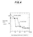
- Fig. 4 shows the molybdenum proportion dependence of the resistivity of tantalum-molybdenum alloy thin films, which were formed on the glass substrate by sputtering with biases of 0 and 500 W and an output of 1.0 kW in an argon gas atmosphere under a pressure of 1.7 mTorr.
- the resistivity of the tantalum-molybdenum alloy thin films that were manufactured without bias was sharply reduced to 40 to 50 [ ⁇ cm] as the molybdenum proportion was increased beyond 15 atomic %.
- the resistivity of the tantalum-molybdenum alloy thin films that were formed with the bias of 500 W was sharply reduced to 50 to 60 [ ⁇ cm] as the molybdenum proportion was incresed beyond 10 atomic %.
- the power output and argon gas atmosphere pressure noted above are by no means limitative; the power may be in a range of 0.1 to 5.0 kW, and the pressure may be in a range of 0.5 to 50 mTorr.
- the lower limits of these conditions of manufacture are prescribed by the conditions which allow stable generation and continuance of electric discharge during the sputtering.
- the upper limit of the pressure is prescribed by the quality of the tantalum-molydenum alloy thin film. The higher the pressure, the surface of the obtained thin film has the greater unevenness. When the pressure is excessive, a low density and porous thin film is formed, which is unsuitable as the electrode thin film.
- Figs. 5(a) to 5(c) show X-ray diffraction patterns of tantalum-molybdenum alloy thin films formed under bias-free condition.
- Fig. 5(a) shows the X-ray diffraction pattern of a tantalum-molybdenum thin film with a molybdenum proportion of 14.2 atomic %.
- Fig. 5(b) shows the X-ray diffraction pattern of a tantalum-molybdenum alloy thin film with a molybdenum proportion of 20.1 atomic %.
- Fig. 5(c) shows the X-ray diffraction pattern of a tantalum-molybdenum alloy thin film with a molybdenum proportion of 25.8 atomic %.
- Figs. 6(a) to 6(c) show X-ray diffraction patterns of tantalum-molybdenum alloy thin films formed with a bias of 500 W.
- Fig. 6(a) shows an X-ray diffraction pattern of a tantalum (Ta) thin flim.
- Fig. 6(b) shows an X-ray diffraction pattern of a tantalum-molybdenum alloy thin film with a molybdenum proportion of 9.2 atomic %.
- Fig. 6(c) shows an X-ray diffraction pattern of a tantalum-molybdenum alloy thin film with a molybdenum proportion of 10.8 atomic %.
- Diffraction peaks that appear near diffraction angles of 33 and 70 degrees correspond to the (0, 0, 2) and (5, 1, 3) planes, respectively, of the tetragonal crystal structure, and a diffraction peak appearing near 38 degrees corresponds to the (1, 1, 0) plane of the body centered cubid crystal structure.
- a high resistivity Ta thin film is of the tetragonal crystal structure
- a tantalum-molybdenum alloy thin film having a sufficiently reduced resistivity is of the body centered cubid crystal structure.
- Tantalum-molybdenum alloy thin films having molybdenum proportions around the value corresponding to sharp reduction of the resistivity are of mixed crystals in which the tetragonal crystal structure and body centered cubid crystal structure are compounded, as is seen from Fig. 5(b) and 6(b).
- the resistivity is not reduced, the X-ray diffraction peak of the thin film that represents a body centered cubid crystal structure with a diffraction angle around 38 degrees is small as is seen from Fig. 6(b).
- the resistivity is reduced, the corresponding X-ray diffraction peak is large.
- Fig. 7 shows the molybdenum proportion dependence of the corrosion potential and corrosion current density of tantalum-molybdenum alloy thin films formed without bias, as determined from anodic polarization characteristic measurements using 0.3 N sulfuric acid as electrolyte.
- the corrosion potential is high compared to the tantalum thin film, indicating that the former thin film is of a nobler metal than the latter thin film.
- the corrosion current density is low with the tantalum-molybdenum alloy thin film compared to the tantalum thin film, and it is increased with increasing molybdenum proportion.
- the structure of crystal is a predominating factor of influence on the magnitude of the corrosion potential, and it is understood that the transition of the tetragonal crystal structure obtained with the tantalum thin film formed by sputtering to the body centered cubid crystal structure obtained with the tantalum-molybdenum alloy thin film, has an effect of increasing the corrosion potential, thus improving the corrosion resistance of the tantalum-molybdenum alloy thin film.
- the corrosion current density is predominatingly dependent on the molybdenum proportion and increased monotonously with increasing molybdenum proportion. This fact supports that an electrochemical reaction that once takes place proceeds more quickly with a thin film having a greater molybdenum proportion. Similar results could be obtained from anodic polarization characteristic measurements.
- a tantalum-molybdenum alloy thin film which comprises a mixed crystal composed of a body centered cubic structure crystal having the same molybdenum proportion as of a tantalum-molybdenum alloy thin film obtained with a bias of 100 W or below and a body centered cubic/tetragonal mixed crystal with a mixed crystal ratio, i.e., a X-ray diffraction peak intensity ratio of the body centered cubid crystal structure (1, 1, 0) plane to the tetragonal crystal structure (0, 0, 2) plane, is 0.5 or below as well as being low in resistivity, less subject to corrosion, slow in electrochemical reaction and excellent in corrosion resistance.
- the molybdenum proportion range is as wide as 10 to 15 atomic % and also that the bias range is as wide as 100 to 500 W. These wide manufacture margins permit stable manufacture.
- a tantalum-molybdenum alloy thin film was formed with zero bias and a power output of 0.5 kW and in an argon gas atmosphere under a pressure of 1.7 mTorr.
- the thin film obtained had a tetragonal crystal structure, a molybdenum proportion of 13.7 atomic % and a resistivity of 170 [ ⁇ cm].
- using the same target a tantalum-molybdenum alloy thin film was formed under conditions of an applied bias of 300 W, power of 0.5 kW and an argon gas atmosphere under a pressure of 1.7 mTorr.
- the thin film obtained had a body centered cubid crystal structure, a molybdenum proportion of 12.2 atomic % and a resistivity of 60 [ ⁇ cm].
- the manufacturing conditions such as the molybdenum proportion of the tantalum-molybdenum alloy target are selected such that the molybdenum proportion of tantalum-molybdenum alloy thin films formed with bias ranging from 0 to 500 W is in a range of 10 to 15 atomic %
- the manufacturing conditions such as the molybdenum proportion of the tantalum-molybdenum alloy target are selected such that the molybdenum proportion of tantalum-molybdenum alloy thin films formed with bias ranging from 0 to 500 W is in a range of 10 to 15 atomic %
- FIG. 8 A second embodiment of the present invention will now be described with reference to Fig. 8.
- This embodiment is structurally the same as the preceding Figs. 1 to 2(a) to 2(c) embodiment except for that in this embodiment a non-magnetic spacer thin film 13 and electrode thin films 17 (17 1 and 17 2 ) are formed in lieu of the non-magnetic spacer thin film 3 and electrode thin films 7 (7 1 and 7 2 ) in the first embodiment.
- a non-magnetic spacer thin film 13 and electrode thin films 17 (17 1 and 17 2 ) are formed in lieu of the non-magnetic spacer thin film 3 and electrode thin films 7 (7 1 and 7 2 ) in the first embodiment.
- the difference of this embodiment will now be described.
- a tantalum-molybdenum alloy thin film with a thickness of 200 angstroms and a molybdenum proportion of 13.7 atomic % and having a tetragonal crystal structure is formed by sputtering using a tantalum-molybdenum target with a molybdenum proportion of 13.0 atomic %, without any applied bias, with a power output of 0.5 kW and in an argon gas atmosphere under a pressure of 1.7 mTorr.
- a tantalum-molybdenum alloy thin film with a thickness of 200 angstroms and a molybdenum proportion of 12.2 atomic % and having a tetragonal crystal structure is formed by sputtering using the same target as for the non-magnetic spacer thin film 13 as described above, with a bias of 300 W and a power output of 0.5 kW and in an argon gas atmosphere under a pressure of 1.7 mTorr.
- the other structures and manufacturing steps other than described above are the same as in the previous first embodiment.
- the resistances of the magnetoresistive effect heads were measured, and it was found that as small value as 15 ⁇ can be obtained stably. Heat generation also could be suppressed to a low level. Readback characteristics were further examined, and satisfactory readback waveforms with less noise due to heat could be obtained.
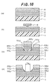
- FIG. 9 A third embodiment of the invention will now be described with reference to Figs. 9 and 10(a) to 10(d).
- This embodiment features that it has a first electrode which constitutes side walls of operative zone Tw and is inclined smoothly.
- this third embodiment has a soft magnetic thin film 2 of a cobalt-zirconium-molybdenum alloy having a thickness of 250 angstroms, a non-magnetic spacer thin film 3 constituted by a tantalum thin film having a thickness of 200 angstroms, and a magnetoresistive effect thin film 4 of a nickel-iron alloy having a thickness of 200 angstroms, these thin films being formed successively by sputtering on an Al 2 O 3 -TiC tye ceramic substrate 1.
- the photoresist 6 was formed to a thickness of 1.2 microns on the laminate, and it was exposed and developed under adequate conditions to form a stencil pattern.
- antiferromagnetic exchange bias thin films 5 (5 1 to 5 3 ) of an iron-manganese alloy having a thickness of 150 angstroms were formed.
- first electrode thin films 7 7 1 to 7 3
- second electrode thin films 8 (8 1 to 8 3 ).
- the material of the second electrode thin films 8 may be selected as desired so long as it has low resistivity and excellent corrosion resistance. Possibly, it may be substituted for by the tantaslum-molybdenum thin film as the first electrode thin films 7 by increasing the total thickness of the thin film to 1 micron.
- the photoresist 6 may be removed more perfectly and more quickly by using ultrasonic wave washing in combination.
- the resistance of the magnetoresistive effect head thus obtained was measured, and it was found that as small value as 15 ⁇ can be obtained stably. Heat generation also could be suppressed to a low level. Readback characteristics were further examined, and satisfactory readback waveforms with less noise due to heat could be obtained.
- FIG. 11 A fourth embodiment will now be described with reference to Fig. 11.
- This fourth embodiment, as shown in Fig. 11, is the same as the preceding Fig. 9 third embodiment except for that in this embodiment a non-magnetic spacer thin film 23 and electrode thin films 27 (27 1 and 27 2 ) are formed in lieu of the non-magnetic spacer thin film 3 and electrode thin films 7 (7 1 and 7 2 ) in the third embodiment.
- a non-magnetic spacer thin film 23 and electrode thin films 27 27 1 and 27 2
- the different part of this embodiment will now be described.
- a tantalum-molybdenum alloy thin film with a thickness of 200 angstroms and a molybdenum proportion of 13.7 atomic % and having a tetragonal crystal structure was formed by sputtering using a tantalum-molybdenum alloy target with a molybdenum proportion of 13.0 atomic %, with no bias and an output of 0.5 kW and in an argon gas atmosphere under a pressure of 1.7 mTorr.
- a tantalum-molybdenum alloy thin film with a thickness of 200 angstroms and a molybdenum proportion of 12.3 atomic % was formed by sputtering using the same target as for the non-mgnetic spacer thin film 23 with a bias of 300 W and an output of 0.5 kW and in an argon gas structure under a pressure of 1.7 mTorr.
- the other structures and manufacturing steps are the same as in the case of the above third embodiment.
- the resistance of the magnetoresistive effect head thus obtained was measured, and it was found that as small value as 15 ⁇ can be obtained stably. Heat generation also could be suppressed to a low level. Readback characteristics were further examined, and and it was found that satisfactory readback waveforms with less noise due to heat are obtainable.
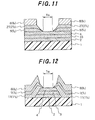
- FIG. 11 A fifth embodiment will now be described with reference to Figs. 11 to 14.
- This embodiment as shown in Fig. 12, features in that its soft magnetic thin film 2, non-magnetic spacer thin film 3 and magnetoresistive effect thin film 4 are tapered. This will now be described.
- soft magnetic thin film 2 of a cobalt-zirconium-molybdenum alloy with a thickness of 250 angstroms, non-magnetic spacer thin film 3 constituted by a tantalum thin film with a thickness of 200 angstroms and a magnetoresistive effect thin film 4 of nickel-iron alloy with a thickness of 200 angstroms, are laminated by sputtering successively on an Al 2 O 3 -TiC type ceramic substrate 1.
- photoresist 6 was coated to a thickness of 1 micron.
- the photoresist 6 was patterned to a width of 3.5 microns through exposure and development under appropriate conditions.
- the stencil shaft portion thin film 10 constituted by the gold thin film was patterned to a width of 1.5 microns through ion milling and etching using an etching solution containing iodine, potassium iodide and water in weight proportions of "1 : 2 : 200".
- the stencil that is formed from the photoresist 6 and stencil shaft portion thin film 10 as shown in Fig. 13(c) may also be formed by using the sole photoresist described before in connection with the previous third embodiment.
- Fig. 14(a) the soft magnetic thin film 2, non-magnetic spacer thin film 3 and magnetoresistive effect thin film 4 were tapered through ion milling with an inclination angle of 45 degrees.
- Fig. 14(b) a hard magnetic tranverse bias thin films 11 (11 1 to 11 3 ) constituted by a cobalt-chromium-platinum thin film with a thickness of 300 angstroms was formed.
- a tantalum-molybdenum alloy thin film with a thickness of 500 angstroms and a molybdenum proportion of 10.8 atomic % and having a body centered cubid crystal structure was sputtering formed as first electrode thin films 7 (7 1 to 7 3 ) on the thin films 11 (11 1 to 11 3 ) with a bias of 500 W and an output of 1.0 kW and in an argon gas atmophere under a pressure of 1.7 mTorr.
- a gold thin film with a thickness of 1 micron was laminated as second electrode thin films 8 (8 1 to 8 3 ) on the thin films 7 (7 1 to 7 3 ).
- the material of the second electrode thin films 8 (8 1 to 8 3 ) may be selected as desired so long as it has low resistivity and excellent corrosion resistance. It may also be substituted for by the tantalum-molybdenum alloy thin film as the first electrode thin films 7 (7 1 to 7 3 ) by increasing the total thickness of the thin film to about 1 micron.
- the photoresist 6 may be removed more perfectly and more quickly by using ultrasonic wave washing of the like in combination.
- the resistance of the magnetoresistive effect head thus obtained was measured, and it was found that as small value as 15 ⁇ can be obtained stably. As for readback characteristics, satisfactory readback waveforms with Less noise due to heat could be obtained.
- FIG. 15 A sixth embodiment will now be described with reference to fig. 15.
- This embodiment is structurally the same as the preceding Fig. 12 fifth embodiment except for that in this embodiment a non-magnetic spacer thin film 33 and electrode thin films 37 (37 1 and 37 2 ) were formed in lieu of the non-magnetic spacer thin film 3 and first electrode thin films 7 (7 1 and 7 2 ) in the fifth embodiment.
- the different part of this embodiment will now be described.
- a tantalum-molybdenum alloy thin film with a thickness of 200 angstroms and a molybdenum proportion of 13.7 atomic % and having a tetragonal crystal structure was formed by sputtering using a tantalum-molybdenum target with a molybdenum proportion of 13.0 atomic %, with no bias and an output of 0.5 kW and in an argon gas atmosphere under a pressure of 1.7 mTorr.
- a tantalum-molybdenum alloy thin film with a thickness of 200 angstroms and a molybdenum proportion of 12.2 artomic % was formed by sputtering using the same target as for the non-magnetic spacer thin film 3, with a bias of 300 W and an output of 0.5 kW and having a tetragonal crystal structure.
- the other structures and manufacturing steps are the same as in the case of the previous fifth embodiment.
- the resistance of the magnetoresistive effect head thus obtained was measured, and it was found that as small value as approximately 15 ⁇ can be obtained stably. Heat generation also could be suppressed to a low level. Readback characteristics were further examined, and it was found that satisfactory readback waveforms with less noise due to heat are obtainable.
- an electrode thin film with as low resistivity as about one-fourth of the resistivity of a tantalum thin film and excellent corrosion resistance is obtainable, thus permitting the provision of a magnetoresistive effect head, which can provide for low resistivity as a head element, generates less heat and noise, has satisfactory corrosion resistance and is highly reliable.
- a high resistivity non-magnetic sacer thin film and a low resistivity electrode thin film can be formed by using the same target, thus permitting stable provision of a high reliability magnetoresistive effect head at a low cost and with a reduced number of steps. It is thus possible to extremely improve the productivity.
Applications Claiming Priority (2)
| Application Number | Priority Date | Filing Date | Title |
|---|---|---|---|
| JP321919/94 | 1994-12-26 | ||
| JP6321919A JP2778494B2 (ja) | 1994-12-26 | 1994-12-26 | 電極薄膜およびその電極薄膜を用いた磁気抵抗効果型ヘッド |
Publications (2)
| Publication Number | Publication Date |
|---|---|
| EP0720154A2 true EP0720154A2 (fr) | 1996-07-03 |
| EP0720154A3 EP0720154A3 (fr) | 1996-09-18 |
Family
ID=18137882
Family Applications (1)
| Application Number | Title | Priority Date | Filing Date |
|---|---|---|---|
| EP95309423A Withdrawn EP0720154A3 (fr) | 1994-12-26 | 1995-12-22 | Electrode à couche mince pour tel qu'une tête à effet magnétorésistif et procédé de fabrication |
Country Status (2)
| Country | Link |
|---|---|
| EP (1) | EP0720154A3 (fr) |
| JP (1) | JP2778494B2 (fr) |
Citations (18)
| Publication number | Priority date | Publication date | Assignee | Title |
|---|---|---|---|---|
| JPS587864A (ja) * | 1981-07-06 | 1983-01-17 | Hitachi Ltd | 半導体装置及びその製造方法 |
| EP0144851A2 (fr) * | 1983-11-24 | 1985-06-19 | Siemens Aktiengesellschaft | Procédé de fabrication de couches de permalloy par pulvérisation |
| US4525262A (en) * | 1982-01-26 | 1985-06-25 | Materials Research Corporation | Magnetron reactive bias sputtering method and apparatus |
| US4622613A (en) * | 1983-10-07 | 1986-11-11 | Matsushita Electric Industrials Co., Ltd. | Thin film magnetic head |
| US4683043A (en) * | 1986-01-21 | 1987-07-28 | Battelle Development Corporation | Cubic boron nitride preparation |
| US4683012A (en) * | 1984-04-18 | 1987-07-28 | Sony Corporation | Magnetic thin film |
| JPS62205656A (ja) * | 1986-03-06 | 1987-09-10 | Toshiba Corp | 半導体装置 |
| EP0236629A2 (fr) * | 1986-03-06 | 1987-09-16 | Kabushiki Kaisha Toshiba | Circuit de commande d'un dispositif d'affichage à cristaux liquides |
| EP0288316A2 (fr) * | 1987-04-23 | 1988-10-26 | Matsushita Electric Industrial Co., Ltd. | Films d'un alliage nitruré de composition modulée et sa méthode de fabrication |
| EP0298840A2 (fr) * | 1987-07-09 | 1989-01-11 | Fujitsu Limited | Support d'enregistrement magnétique et sa méthode de fabrication |
| JPH02278879A (ja) * | 1989-04-20 | 1990-11-15 | Toshiba Corp | 薄膜トランジスタの製造方法 |
| DE4021376A1 (de) * | 1989-07-05 | 1991-01-17 | Toshiba Kawasaki Kk | Magnetkopf und verfahren zu seiner herstellung |
| EP0435325A2 (fr) * | 1989-12-29 | 1991-07-03 | Sony Corporation | Films minces magnétiquement doux à base de Fe-N et têtes magnétiques utilisant de tels films |
| US5140403A (en) * | 1990-02-27 | 1992-08-18 | Fuji Xerox Co., Ltd. | Thin-film semiconductor device having an α-tantalum first wiring member |
| EP0534425A2 (fr) * | 1991-09-25 | 1993-03-31 | Canon Kabushiki Kaisha | Dispositif photovoltaique |
| EP0552890A2 (fr) * | 1992-01-21 | 1993-07-28 | International Business Machines Corporation | Capteur magnétique |
| US5268806A (en) * | 1992-01-21 | 1993-12-07 | International Business Machines Corporation | Magnetoresistive transducer having tantalum lead conductors |
| US5290731A (en) * | 1991-03-07 | 1994-03-01 | Sony Corporation | Aluminum metallization method |
Family Cites Families (4)
| Publication number | Priority date | Publication date | Assignee | Title |
|---|---|---|---|---|
| JPS539198B2 (fr) * | 1972-10-31 | 1978-04-04 | ||
| JPH07105486B2 (ja) * | 1986-09-05 | 1995-11-13 | 株式会社東芝 | 電極配線材料 |
| JP2503688B2 (ja) * | 1989-11-10 | 1996-06-05 | 日本電気株式会社 | 薄膜トランジスタの製造方法 |
| JPH06267659A (ja) * | 1993-03-09 | 1994-09-22 | Oki Electric Ind Co Ltd | 薄膜elパネルのタングステン電極の形成方法 |
-
1994
- 1994-12-26 JP JP6321919A patent/JP2778494B2/ja not_active Expired - Fee Related
-
1995
- 1995-12-22 EP EP95309423A patent/EP0720154A3/fr not_active Withdrawn
Patent Citations (18)
| Publication number | Priority date | Publication date | Assignee | Title |
|---|---|---|---|---|
| JPS587864A (ja) * | 1981-07-06 | 1983-01-17 | Hitachi Ltd | 半導体装置及びその製造方法 |
| US4525262A (en) * | 1982-01-26 | 1985-06-25 | Materials Research Corporation | Magnetron reactive bias sputtering method and apparatus |
| US4622613A (en) * | 1983-10-07 | 1986-11-11 | Matsushita Electric Industrials Co., Ltd. | Thin film magnetic head |
| EP0144851A2 (fr) * | 1983-11-24 | 1985-06-19 | Siemens Aktiengesellschaft | Procédé de fabrication de couches de permalloy par pulvérisation |
| US4683012A (en) * | 1984-04-18 | 1987-07-28 | Sony Corporation | Magnetic thin film |
| US4683043A (en) * | 1986-01-21 | 1987-07-28 | Battelle Development Corporation | Cubic boron nitride preparation |
| JPS62205656A (ja) * | 1986-03-06 | 1987-09-10 | Toshiba Corp | 半導体装置 |
| EP0236629A2 (fr) * | 1986-03-06 | 1987-09-16 | Kabushiki Kaisha Toshiba | Circuit de commande d'un dispositif d'affichage à cristaux liquides |
| EP0288316A2 (fr) * | 1987-04-23 | 1988-10-26 | Matsushita Electric Industrial Co., Ltd. | Films d'un alliage nitruré de composition modulée et sa méthode de fabrication |
| EP0298840A2 (fr) * | 1987-07-09 | 1989-01-11 | Fujitsu Limited | Support d'enregistrement magnétique et sa méthode de fabrication |
| JPH02278879A (ja) * | 1989-04-20 | 1990-11-15 | Toshiba Corp | 薄膜トランジスタの製造方法 |
| DE4021376A1 (de) * | 1989-07-05 | 1991-01-17 | Toshiba Kawasaki Kk | Magnetkopf und verfahren zu seiner herstellung |
| EP0435325A2 (fr) * | 1989-12-29 | 1991-07-03 | Sony Corporation | Films minces magnétiquement doux à base de Fe-N et têtes magnétiques utilisant de tels films |
| US5140403A (en) * | 1990-02-27 | 1992-08-18 | Fuji Xerox Co., Ltd. | Thin-film semiconductor device having an α-tantalum first wiring member |
| US5290731A (en) * | 1991-03-07 | 1994-03-01 | Sony Corporation | Aluminum metallization method |
| EP0534425A2 (fr) * | 1991-09-25 | 1993-03-31 | Canon Kabushiki Kaisha | Dispositif photovoltaique |
| EP0552890A2 (fr) * | 1992-01-21 | 1993-07-28 | International Business Machines Corporation | Capteur magnétique |
| US5268806A (en) * | 1992-01-21 | 1993-12-07 | International Business Machines Corporation | Magnetoresistive transducer having tantalum lead conductors |
Non-Patent Citations (7)
| Title |
|---|
| DATABASE WPI Section Ch, Week 7444 Derwent Publications Ltd., London, GB; Class L02, AN 74-76580V XP002008335 & JP-A-49 069 597 (NIHON SHINKU GIJUTSU CO) , 5 July 1974 * |
| DATABASE WPI Section Ch, Week 9211 Derwent Publications Ltd., London, GB; Class L03, AN 92-086542 XP002008336 ANONYMOUS: "Improving soft-bias film properties in magnetoresistive sensor - comprises adding small amt. of nitrogen to argon sputtering gas during deposition of soft magnetic layer with transverse bias" & RESEARCH DISCLOSURE, vol. 334, no. 079, 10 February 1992, EMSWORTH, GB, * |
| JAPANESE JOURNAL OF APPLIED PHYSICS, vol. 33, no. 7A, 1 July 1994, pages 4086-4089, XP000565300 OSHIO S ET AL: "STRESS AND RESISTIVITY OF TA-MO AND TA-W SPUTTERED THIN FILMS" * |
| JOURNAL OF THE ELECTROCHEMICAL SOCIETY, JULY 1985, USA, vol. 132, no. 7, ISSN 0013-4651, pages 1689-1694, XP000567710 OHFUJI S ET AL: "Reduction of sodium ion density in molybdenum-gate MOS devices with the addition of tantalum to gate electrodes" * |
| PATENT ABSTRACTS OF JAPAN vol. 007, no. 080 (E-168), 2 April 1983 & JP-A-58 007864 (HITACHI SEISAKUSHO KK), 17 January 1983, * |
| PATENT ABSTRACTS OF JAPAN vol. 012, no. 063 (E-585), 25 February 1988 & JP-A-62 205656 (TOSHIBA CORP), 10 September 1987, * |
| PATENT ABSTRACTS OF JAPAN vol. 015, no. 046 (E-1029), 4 February 1991 & JP-A-02 278879 (TOSHIBA CORP), 15 November 1990, * |
Also Published As
| Publication number | Publication date |
|---|---|
| JPH08180335A (ja) | 1996-07-12 |
| JP2778494B2 (ja) | 1998-07-23 |
| EP0720154A3 (fr) | 1996-09-18 |
Similar Documents
| Publication | Publication Date | Title |
|---|---|---|
| CN102965719B (zh) | 薄膜金属和合金的低速率电化学蚀刻 | |
| EP0583889B1 (fr) | Procédé de décapage d'un motif dans des couches de Sendust et de chrome | |
| US6063512A (en) | Soft magnetic thin film having Co, Ni and Fe as main ingredients, method of manufacturing the same and magnetic head and magnetic storage unit using the soft magnetic thin film | |
| Neff et al. | Structural, optical, and electronic properties of magnetron‐sputtered platinum oxide films | |
| US4390404A (en) | Process for manufacture of thin-film magnetic bubble domain detection device | |
| US4208257A (en) | Method of forming an interconnection | |
| US4402801A (en) | Method for manufacturing thin film magnetic head | |
| US5680091A (en) | Magnetoresistive device and method of preparing the same | |
| EP0720154A2 (fr) | Electrode à couche mince pour tel qu'une tête à effet magnétorésistif et procédé de fabrication | |
| JPS6222247B2 (fr) | ||
| US6477006B1 (en) | Thin-film magnetic head for track width not more than 1 μm on recording medium and method for making the same | |
| US6692847B2 (en) | Magneto resistive sensor | |
| US5510941A (en) | Magneto-resistive type magnetic head with a shunt layer of molybdenum | |
| US8310788B2 (en) | Protective film forming method | |
| US6055135A (en) | Exchange coupling thin film and magnetoresistive element comprising the same | |
| EP0418127A1 (fr) | Procédé de réalisation des pièces polaires et de l'entrefer de têtes magnÀ©tiques en couches minces pour application informatique audio ou vidéo | |
| EP0016263A1 (fr) | Résistance en couche mince à coefficient de température élevé et procédé pour sa fabrication | |
| JP2001076314A (ja) | 薄膜磁気ヘッドの製造方法 | |
| US4699702A (en) | Process for preparing soft magnetic film of Permalloy | |
| JP2790109B2 (ja) | 裏面からの成分分析の試料作成方法 | |
| DE2456384B2 (de) | Verfahren zur Herstellung einer Dünnschichtelektrode in einem Fühlelement zur Bestimmung einer Abweichung vom Lot | |
| JPH01169367A (ja) | 微小電極抵抗測定用プローブ | |
| Kudo et al. | Electrochemical behaviour of Ni+ Al alloy as an alternative material for molten carbonate fuel cell cathodes | |
| JP3353281B2 (ja) | 誘電体光学材料の微細加工方法 | |
| JP2806317B2 (ja) | 永久磁石膜およびそれを用いた磁気抵抗効果ヘッド |
Legal Events
| Date | Code | Title | Description |
|---|---|---|---|
| PUAI | Public reference made under article 153(3) epc to a published international application that has entered the european phase |
Free format text: ORIGINAL CODE: 0009012 |
|
| AK | Designated contracting states |
Kind code of ref document: A2 Designated state(s): DE FR GB |
|
| PUAL | Search report despatched |
Free format text: ORIGINAL CODE: 0009013 |
|
| AK | Designated contracting states |
Kind code of ref document: A3 Designated state(s): DE FR GB |
|
| 17P | Request for examination filed |
Effective date: 19970218 |
|
| 17Q | First examination report despatched |
Effective date: 19990527 |
|
| STAA | Information on the status of an ep patent application or granted ep patent |
Free format text: STATUS: THE APPLICATION IS DEEMED TO BE WITHDRAWN |
|
| 18D | Application deemed to be withdrawn |
Effective date: 19991007 |