EP0718872A1 - Semiconductor substrate cleaning method - Google Patents
Semiconductor substrate cleaning method Download PDFInfo
- Publication number
- EP0718872A1 EP0718872A1 EP95305651A EP95305651A EP0718872A1 EP 0718872 A1 EP0718872 A1 EP 0718872A1 EP 95305651 A EP95305651 A EP 95305651A EP 95305651 A EP95305651 A EP 95305651A EP 0718872 A1 EP0718872 A1 EP 0718872A1
- Authority
- EP
- European Patent Office
- Prior art keywords
- semiconductor substrate
- pure water
- oxygen concentration
- cleaning method
- substrate cleaning
- Prior art date
- Legal status (The legal status is an assumption and is not a legal conclusion. Google has not performed a legal analysis and makes no representation as to the accuracy of the status listed.)
- Granted
Links
Images




Classifications
-
- H—ELECTRICITY
- H10—SEMICONDUCTOR DEVICES; ELECTRIC SOLID-STATE DEVICES NOT OTHERWISE PROVIDED FOR
- H10P—GENERIC PROCESSES OR APPARATUS FOR THE MANUFACTURE OR TREATMENT OF DEVICES COVERED BY CLASS H10
- H10P52/00—Grinding, lapping or polishing of wafers, substrates or parts of devices
-
- H—ELECTRICITY
- H10—SEMICONDUCTOR DEVICES; ELECTRIC SOLID-STATE DEVICES NOT OTHERWISE PROVIDED FOR
- H10P—GENERIC PROCESSES OR APPARATUS FOR THE MANUFACTURE OR TREATMENT OF DEVICES COVERED BY CLASS H10
- H10P70/00—Cleaning of wafers, substrates or parts of devices
- H10P70/10—Cleaning before device manufacture, i.e. Begin-Of-Line process
- H10P70/15—Cleaning before device manufacture, i.e. Begin-Of-Line process by wet cleaning only
-
- B—PERFORMING OPERATIONS; TRANSPORTING
- B08—CLEANING
- B08B—CLEANING IN GENERAL; PREVENTION OF FOULING IN GENERAL
- B08B3/00—Cleaning by methods involving the use or presence of liquid or steam
- B08B3/04—Cleaning involving contact with liquid
- B08B3/10—Cleaning involving contact with liquid with additional treatment of the liquid or of the object being cleaned, e.g. by heat, by electricity or by vibration
Definitions
- the present invention relates to a semiconductor substrate cleaning method for use in a fabrication process for a semiconductor device, and to a semiconductor device fabrication method using the cleaning method.
- An object of the present invention is to provide a semiconductor substrate cleaning method which can effectively remove contaminants and residual chemicals without increasing the number of chemical treatment steps and/or enable a semiconductor device of high quality to be fabricated after use of the semiconductor substrate cleaning method without lowering product yields.
- a semiconductor substrate cleaning method in which a semiconductor substrate is immersed in pure water having a lowered dissolved-oxygen concentration and a temperature above 60°C under an atmosphere which controls oxygen concentration to maintain such dissolved oxygen concentration in the pure water, whereby the semiconductor substrate is cleaned to remove oxide film on the surface thereof.
- the atmosphere under which it is carried out be shielded from the outside air so that the dissolved oxygen concentration in the pure water is maintained.
- the oxygen concentration in such atmosphere is adjusted so that the dissolved oxygen concentration in the pure water is maintained.
- the dissolved oxygen concentration in the pure water is, for its part, preferably below 200 ppb at room temperature.
- the semiconductor substrate is immersed in the pure water for at least 10 minutes.
- the pure water itself is preferably at a temperature of at least 80°C, more preferably at least 90°C.
- the above-described semiconductor substrate cleaning method is carried out with the temperature of the pure water and the time during which the semiconductor substrate is immersed in the pure water such that, after cleaning, the semiconductor substrates form a contact angle of above 70°.
- the above-described semiconductor substrate cleaning method is particularly applicable to removal of oxide film on the surface of the semiconductor substrate which results from immersing the semiconductor substrate in a chemical solution.
- a chemical solution used in association with the semiconductor substrate cleaning method is preferably a mixture of ammonium hydroxide, hydrogen peroxide and pure water and may be a cause of such oxide film.
- the method of this invention may be applied to removal of oxide films on the surface of the semiconductor substrate which is native oxide films formed as a result of exposure of the semiconductor substrate to the oxygen-containing atmosphere, or resulting from immersing the semiconductor substrate in pure water having a higher dissolved oxygen concentration than said pure water.
- the above-described method may be utilised in a semiconductor device fabrication method including a step of cleaning surfaces of semiconductor substrates.
- semiconductor substrates are immersed in pure water having a low dissolved oxygen concentration and heated to a temperature above 60°C, under an atmosphere such that the dissolved oxygen concentration in the pure water is maintained to cause oxide films on the surfaces of the semiconductor substrates to be removed therefrom.
- contaminants and residual chemicals can be effectively removed without adding any chemical treating step.
- the cleaning can be effective without increasing the number of chemicals, and improved throughputs can be obtained in the cleaning step.
- a semiconductor substrate cleaning method embodying the present invention, and semiconductor substrate cleaning equipment in which it is to be used, will be explained with reference to FIGs. 1 to 14. First the structure of the cleaning equipment used in the present embodiment will be explained.
- FIG. 1 is a diagrammatic view of semiconductor substrate cleaning equipment to be used in carrying out the method of the present invention.
- the cleaning equipment is enclosed by a housing 10 so that the inside of the cleaning equipment is shielded from the outside air.
- a pure water bath 12 for cleaning semiconductor substrates, and a heater 14 which heats a cleaning liquid to be fed into the pure water bath 12.
- the pure water bath 12 has a pure water feed pipe 16 which supplies pure water thereto.
- the pure water feed pipe 16 is connected to a DO (dissolved oxygen) meter which detects dissolved oxygen concentration in the pure water to be supplied to the pure water bath 12.
- DO dissolved oxygen
- a differential pressure gauge 28 which measures pressure differences between the outside of the housing and the inside of the housing 10, a nitrogen feed pipe 20 and an oxygen feed pipe 22, so that the conditions in the inside of the housing can be controlled.
- oxygen concentrations in the housing 10 are monitored by an oxygen concentration meter 24 and are controlled to be below 25 ppm at 25°C.
- the inside of the cleaning equipment is thus shielded from the outside to enable the conditions in the equipment to be controlled since, otherwise, when pure water having a low dissolved oxygen content is left exposed to the external atmosphere, oxygen in the atmospheric air dissolves in the pure water and the dissolved oxygen concentration cannot be kept low.
- the housing 10 has an external chamber 26 which prevents the external atmosphere from coming into the housing 10 when semiconductor substrates are being loaded into the housing 10.
- semiconductor substrates When semiconductor substrates are loaded into the housing 10, they are first temporarily supplied to the chamber 26, and the atmosphere in the chamber 26 is replaced by an inert gas atmosphere, e.g., nitrogen. Only then are the semiconductor substrates loaded into the housing 10.
- an inert gas atmosphere e.g., nitrogen. Only then are the semiconductor substrates loaded into the housing 10.
- FIG. 2 shows the dependency of the amount of residual metallic contamination on the dissolved oxygen content of pure water.
- FIG. 3 shows the dependency of the amount of residual metallic contamination on the treatment temperature.
- FIG.4 shows the dependency of the amount of residual metallic contamination on the treatment time.
- FIG. 2 shows the relationship between dissolved oxygen concentration and the cleaning effect measured when semiconductor substrates were immersed in pure water having a temperature of 100°C for 30 minutes.
- metallic contaminants were applied to the surfaces of the semiconductor substrates before the cleaning in a pretreatment step in which p-type and n-type (100)-oriented silicon substrates having a resistivity about 10 ⁇ -cm were first treated with hydrogen fluoride to remove oxide films on the surfaces of the semiconductor substrates, and then immersed in an SC-1 solution added to an atomic absorption spectrometry standard solution containing Al, Cd, Co, Cr, Cu, Fe, Mg, Mn and Ni to achieve the chemical treatment of the substrates.
- FIG. 3 shows the relationship between pure water temperature and the cleaning effect measured when dissolved oxygen concentration in the pure water was 1 ppb and the treatment time was 30 minutes.
- the metallic contaminant removing effect does not change much with treatment temperature.
- the treatment temperature is above 60°C, the effect on metallic contaminant removal was improved for all metals except Cu.
- the contaminant removing effect sharply increased when the treatment temperature rose to above 80°C.
- the treatment temperature was raised above 90°C, the contaminant removing effect improved further and the amount of Al contaminant, whose removal had not increased much previously, decreased to below 1/10 of initial amount.
- the adsorption amounts of metallic contaminants except Cu steadily decreased in the first 10 minutes of the treatment and decreased further with further increases in the immersion time. However, after 30 minutes, the adsorption amounts of contaminants did not decrease further and thereafter no substantial changes took place in the adsorbed amounts. Thus, the removal of metallic contaminants by the use of low dissolved-oxygen pure water is considered to reach equilibrium.
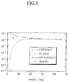
- FIG. 5 shows the depth profile of the contaminant Al on semiconductor substrates processed in accordance with the method of this invention as measured by XPS (X-ray photoelectron spectroscopy).
- FIG. 6A shows the result of TRXF (total reflection X-ray fluorescence analysis) observation on the contaminated semiconductor substrates.
- FIG. 6B assists in explaining FIG. 6A.
- FIG. 7 is a graph showing the relationship between the contact angle of the cleaned semiconductor substrate and treatment temperatures.
- FIG. 8 shows the change in the FT-IR RAS spectra after immersion in pure water having a lower dissolved oxygen concentration.
- FIG. 9 is a graph showing the relationship between contact angles of the cleaned semiconductor substrates and treatment temperatures.
- FIG. 10 shows the change in the FT-IR RAS spectra after immersion in pure water having a lower dissolved oxygen concentration.
- FIG. 11 is a graph showing amounts of residual sulfuric acid ions on the cleaned semiconductor substrates.
- measured depth profile values for metallic contaminants in the contaminated samples prepared by the present embodiment will be considered.
- FIG. 5 shows the depth profile of the contaminant Al measured by XPS, at the surface of semiconductor substrates immediately after contamination.
- the dotted line indicates interfaces between oxide films and the semiconductor substrates
- the dot chain line indicates the surfaces of the oxide films.
- Al is present as metallic contaminant in the oxide films and near the surface of the semiconductor substrate.
- FIG. 6A shows the result of TRXF observation on the surfaces of the semiconductor substrate immediately after contamination.
- FIG. 6B shows how metallic contamination has different peak positions depending on particle contamination or molecular surface contamination. All the metallic contaminants have increasing intensities with increases of incident angles of X-rays, the metallic contaminants being present in molecular states.
- FIG. 7 shows the relationship between treatment temperature and contact angle at the wafer surfaces for a dissolved oxygen concentration in the pure water set at 1 ppb and with treatment time set at 30 minutes.
- the surfaces of the semiconductor substrates are hydrophilic because of grown oxide films, i.e., they have small contact angles (indicated by ⁇ in FIG. 7).
- contact angles gradually increased with higher treatment temperatures. The changes were small at temperatures below 90°C and the semiconductor substrate surfaces remained hydrophilic.
- contact angles greatly increased and the semiconductor substrate surfaces became hydrophobic.
- the surface state of the semiconductor substrates at this time were estimated by FT-IR. As shown in FIG. 8, it was found that peak amounts of Si-O bonds observed at treatment temperatures below 70°C disappeared at a 100°C treatment temperature, and oxide films were removed.
- the dissolved oxygen concentration in the pure water was set to 1 ppb, and the treatment time was set at 30 minutes, the amounts of metals absorbed on the semiconductor substrate surfaces were greatly decreased.
- the change in the semiconductor substrate surfaces from hydrophilic to hydrophobic is considered to be due to the oxide films on the semiconductor substrate surfaces being removed.
- the metallic contaminants absorbed on the semiconductor substrate surfaces were removed.
- the equilibrium stage in the removal of contaminants as seen FIG. 4 is considered to be due to the oxide films having all been removed.
- FIG. 11 shows the amount of residual sulfuric acid ions after the semiconductor substrates have been immersed in a mixture of hydrogen peroxide and sulfuric acid and then cleaned with various kinds of pure water.
- Treatment A is a treatment with 8 ppb dissolved-oxygen concentration in 25°C pure water after a chemical treatment.
- Treatment B is a treatment with 1 ppb dissolved-oxygen concentration in 25°C pure water.
- Treatment C is a treatment with 1 ppb dissolved-oxygen concentration in 100°C pure water after a chemical treatment.
- a reference wafer was treated with a mixed liquid of ammonium hydroxide and hydrogen peroxide, and next treated with nitric acid.
- Treatment C can be seen to reduce the residual sulfuric acid ion density down to about 1/10 that achieved in treatments A and B.
- the sulfuric acid density was reduced substantially to the level of the residual sulfuric acid ion density of the reference wafer.
- the method according to the present embodiment can be applied to cleaning of chemicals from the surfaces of semiconductor substrates by the use of pure water of a low dissolved-oxygen concentration. Accordingly, both contaminants and residual chemicals can be effectively removed without the need to employ chemical treatment steps.
- the cleaning of semiconductor substrates by the use of pure water of low dissolved-oxygen concentration does not require chemicals of high viscosity.
- the surfaces of semiconductor substrates can be cleaned to remove completely residual chemicals.
- Water cleaning with the above-described low dissolved-oxygen concentration pure water following a chemical treatment can effectively reduce residual chemicals in comparison with water cleaning with pure water having a dissolved oxygen concentration not controlled or in comparison with dissolved oxygen pure water at below 60°C.
- the cleaning method can remove contaminants without residual chemicals, and semiconductor devices of high quality can be produced without lowering product yields.
- cleaning of so-called chemical oxide films formed by SC-1 treatment from semiconductor substrates has been explained.
- Cleaning of oxide films on the surfaces of semiconductor substrates may be carried out with low dissolved-oxygen pure water to remove native oxide films formed by leaving semiconductor substrates in an atmosphere containing oxygen or immersing the semiconductor substrates in pure water with a higher dissolved-oxygen amount.
- cleaning is conducted with low dissolved-oxygen pure water for cleaning of the surfaces of semiconductor substrates concurrent with removal of native oxide films.
- contaminants adhered to the surfaces of semiconductor substrates can be removed by immersing the substrates for more than 10 minutes in pure water having a below 200 ppb dissolved oxygen concentration and which has been heated to above 60°C. It is preferred that the precise conditions employed are optimized in accordance with equipment used.
- the temperature of the pure water and the period of time during which semiconductor substrates are immersed are set so that the contact angle formed between the pure water and the semiconductor substrates, more particularly between pure water and a silicon substrate, with no oxide film formed thereon, all oxide film having been removed, is above 70° after cleaning the semiconductor substrate.
- the contact angle formed between the pure water and the semiconductor substrates, more particularly between pure water and a silicon substrate, with no oxide film formed thereon, all oxide film having been removed is above 70° after cleaning the semiconductor substrate.
- semiconductor substrate cleaning equipment is constituted by a chemical bath 30 and a pure water bath 12, the latter being provided in the closed interior of a housing 10 or the like disposed in a usual draft chamber.
- Semiconductor substrates 32 are subjected to a chemical treatment in the chemical bath 30, then loaded into the closed unit in which an atmosphere of adjusted oxygen concentration is established, and are subjected to water cleaning by low dissolved-oxygen pure water in the pure water bath 12.
- a chamber 26 is provided between the closed unit and the outside atmosphere as shown in FIG. 1. In this way, the cleaning can be conducted without disturbing the gas atmosphere in the closed unit.
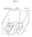
- the chemical bath 30 and the pure water bath 12 be disposed in the same closed unit under an atmosphere having an adjusted oxygen concentration.
- the atmosphere in the housing 10 was controlled so that the oxygen concentration was below 25 ppm at 25°C and atmospheric pressure. It is preferred, however, to control the oxygen concentration in the atmosphere used so that the oxygen concentration in the closed unit can maintain dissolved oxygen concentration in the pure water at a desired low level. Thus, the oxygen concentration in the atmosphere is controlled so as to satisfy Henry's law.
- the pure water bath is provided in the closed unit to prevent outside oxygen from dissolving in the low dissolved-oxygen pure water used for obtaining a high cleaning effect. It is not essential to have the pure water bath within the closed unit as long as the cleaning equipment is such that the low dissolved-oxygen pure water is kept out of contact with outside oxygen.
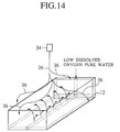
- an inert gas injection port 34 (there may be more than one) is provided above the pure water bath 12, so that inert gas streams are generated which cover the surface of the pure water bath 12 with the inert gas are generated. Outside air does not dissolve in the low dissolved-oxygen pure water, and semiconductor substrates can be cleaned with the dissolved oxygen concentration kept low.
- inert gas injection ports are provided in the walls of the pure water bath, or near the pure water bath and above the surface of the pure water, and inert gas exhaust ports are provided opposed to the injection ports across the pure water bath, so that the inert gas is caused to flow horizontally.
- the low dissolved-oxygen pure water is heated by the heater 14 provided in the pure water bath 12.
- pure water may be heated on passage through heating means 38 before being fed into the cleaning equipment. In this case, overflow rinse, etc. with the low dissolved oxygen pure water is possible. This ensures that removed contaminants do not remain in the pure water bath 12 and may enhance the contaminant removing effect.
Landscapes
- Cleaning Or Drying Semiconductors (AREA)
Abstract
Description
- The present invention relates to a semiconductor substrate cleaning method for use in a fabrication process for a semiconductor device, and to a semiconductor device fabrication method using the cleaning method.
- Increasingly, the semiconductor device fabrication industry has come to need to produce semiconductor integrated circuits of high quality both efficiently and without lowering throughputs and yields. To this end, more effective semiconductor substrate cleaning methods are being developed.
- In the conventional generally used semiconductor substrate cleaning method, chemical cleaning by immersion in many kinds of chemicals and water cleaning are repeated so as to remove contaminants, such as particles, metallic contaminants, organic substances, etc.
- In the usual conventional semiconductor substrate cleaning methods, the more the chemical treatment steps the greater the cleaning time. This results in lower throughputs and has been a problem.
- Moreover, when using a cleaning chemical of high viscosity, the usual water cleaning carried out subsequently cannot fully remove the treatment chemical. This, too, lowers product yields and has been also a problem.
- An object of the present invention is to provide a semiconductor substrate cleaning method which can effectively remove contaminants and residual chemicals without increasing the number of chemical treatment steps and/or enable a semiconductor device of high quality to be fabricated after use of the semiconductor substrate cleaning method without lowering product yields.
- According to the present invention, there is provided a semiconductor substrate cleaning method in which a semiconductor substrate is immersed in pure water having a lowered dissolved-oxygen concentration and a temperature above 60°C under an atmosphere which controls oxygen concentration to maintain such dissolved oxygen concentration in the pure water, whereby the semiconductor substrate is cleaned to remove oxide film on the surface thereof.
- In the above-described semiconductor substrate cleaning method, it is preferable that the atmosphere under which it is carried out be shielded from the outside air so that the dissolved oxygen concentration in the pure water is maintained. Indeed, it is preferable that the oxygen concentration in such atmosphere is adjusted so that the dissolved oxygen concentration in the pure water is maintained.
- The dissolved oxygen concentration in the pure water is, for its part, preferably below 200 ppb at room temperature.
- When carrying out the above-described semiconductor substrate cleaning method, it is preferable that the semiconductor substrate is immersed in the pure water for at least 10 minutes. The pure water itself is preferably at a temperature of at least 80°C, more preferably at least 90°C.
- In a preferred embodiment of the invention the above-described semiconductor substrate cleaning method is carried out with the temperature of the pure water and the time during which the semiconductor substrate is immersed in the pure water such that, after cleaning, the semiconductor substrates form a contact angle of above 70°.
- The above-described semiconductor substrate cleaning method is particularly applicable to removal of oxide film on the surface of the semiconductor substrate which results from immersing the semiconductor substrate in a chemical solution. A chemical solution used in association with the semiconductor substrate cleaning method is preferably a mixture of ammonium hydroxide, hydrogen peroxide and pure water and may be a cause of such oxide film. Alternatively, the method of this invention may be applied to removal of oxide films on the surface of the semiconductor substrate which is native oxide films formed as a result of exposure of the semiconductor substrate to the oxygen-containing atmosphere, or resulting from immersing the semiconductor substrate in pure water having a higher dissolved oxygen concentration than said pure water.
- The above-described method may be utilised in a semiconductor device fabrication method including a step of cleaning surfaces of semiconductor substrates.
- In summary, thus, in the practice of this invention, semiconductor substrates are immersed in pure water having a low dissolved oxygen concentration and heated to a temperature above 60°C, under an atmosphere such that the dissolved oxygen concentration in the pure water is maintained to cause oxide films on the surfaces of the semiconductor substrates to be removed therefrom. As a result, contaminants and residual chemicals can be effectively removed without adding any chemical treating step. The cleaning can be effective without increasing the number of chemicals, and improved throughputs can be obtained in the cleaning step.
- For a better understanding of the invention, and to show how the same can be carried into effect, reference will now be made, by way of example only, to the accompanying drawings, wherein:-
- FIG. 1 shows a diagrammatic view of semiconductor substrate cleaning equipment for use in a method embodying the present invention;
- FIG. 2 set out graphs of relationships between the amount of adsorbed metal on semiconductor substrates cleaned by a semiconductor substrate cleaning method embodying the present invention, and dissolved oxygen concentration;
- FIG. 3 sets out graphs of relationships between amounts of adsorbed metal on semiconductor substrates cleaned by a semiconductor substrate cleaning method embodying the present invention, and treatment temperatures;
- FIG. 4 sets out graphs of relationships between amounts of adsorbed metal on semiconductor substrates cleaned by a semiconductor substrate cleaning method embodying the present invention, and treatment time;
- FIG. 5 sets out a graph indicating the depth profile of the contaminant Al of a semiconductor substrate prepared by a method embodying the present invention, the depth profile values being measured by XPS;
- FIG. 6A sets out a graph indicating the result of TRXF measurements carried out on contaminated semiconductor substrates prepared in a method embodying the present invention;
- FIG. 6B is a graph to be considered in achieving an understanding of the significance of FIG. 6A;
- FIG. 7 is a graph showing the relationship between contact angle with the semiconductor substrates cleaned by a semiconductor substrate cleaning method embodying the present invention, and treatment temperatures;
- FIG. 8 shows FT-IR RAS spectra measured on a semiconductor substrate cleaned by a semiconductor substrate cleaning method embodying the present invention, before and after immersion in pure water having a lower dissolved oxygen concentration;
- FIG. 9 is a graph showing the relationship between contact angles with the semiconductor substrates cleaned by a semiconductor substrate cleaning method embodying the present invention, and treatment time;
- FIG. 10 shows FT-IR RAS spectra measured on a semiconductor substrate cleaned by a semiconductor substrate cleaning method embodying the present invention, before and after immersion in pure water having a lower dissolved oxygen concentration;
- FIG. 11 is a graph showing residual sulfuric acid ion amounts on semiconductor substrates cleaned by a semiconductor substrate cleaning method embodying the present invention;
- FIG. 12 is a schematic view of a first form of semiconductor substrate cleaning equipment for use when carrying out the method of the present invention;
- FIG. 13 is a schematic view of a second form of semiconductor substrate cleaning equipment for use when carrying out the method of the present invention; and
- FIG. 14 shows a schematic view of a third form of semiconductor substrate cleaning equipment for use when carrying out the method of the present invention.
- A semiconductor substrate cleaning method embodying the present invention, and semiconductor substrate cleaning equipment in which it is to be used, will be explained with reference to FIGs. 1 to 14. First the structure of the cleaning equipment used in the present embodiment will be explained.
- FIG. 1 is a diagrammatic view of semiconductor substrate cleaning equipment to be used in carrying out the method of the present invention. The cleaning equipment is enclosed by a
housing 10 so that the inside of the cleaning equipment is shielded from the outside air. In thebox 10 there are provided apure water bath 12 for cleaning semiconductor substrates, and aheater 14 which heats a cleaning liquid to be fed into thepure water bath 12. Thepure water bath 12 has a purewater feed pipe 16 which supplies pure water thereto. The purewater feed pipe 16 is connected to a DO (dissolved oxygen) meter which detects dissolved oxygen concentration in the pure water to be supplied to thepure water bath 12. - Outside the
box 10, there are provided adifferential pressure gauge 28 which measures pressure differences between the outside of the housing and the inside of thehousing 10, anitrogen feed pipe 20 and an oxygen feed pipe 22, so that the conditions in the inside of the housing can be controlled. In the illustrated arrangement, oxygen concentrations in thehousing 10 are monitored by anoxygen concentration meter 24 and are controlled to be below 25 ppm at 25°C. - The inside of the cleaning equipment is thus shielded from the outside to enable the conditions in the equipment to be controlled since, otherwise, when pure water having a low dissolved oxygen content is left exposed to the external atmosphere, oxygen in the atmospheric air dissolves in the pure water and the dissolved oxygen concentration cannot be kept low.
- The
housing 10 has anexternal chamber 26 which prevents the external atmosphere from coming into thehousing 10 when semiconductor substrates are being loaded into thehousing 10. When semiconductor substrates are loaded into thehousing 10, they are first temporarily supplied to thechamber 26, and the atmosphere in thechamber 26 is replaced by an inert gas atmosphere, e.g., nitrogen. Only then are the semiconductor substrates loaded into thehousing 10. - The method of cleaning semiconductor substrates using the semiconductor substrate cleaning equipment will now be explained.
- FIG. 2 shows the dependency of the amount of residual metallic contamination on the dissolved oxygen content of pure water. FIG. 3 shows the dependency of the amount of residual metallic contamination on the treatment temperature. FIG.4 shows the dependency of the amount of residual metallic contamination on the treatment time.
- More specifically, FIG. 2 shows the relationship between dissolved oxygen concentration and the cleaning effect measured when semiconductor substrates were immersed in pure water having a temperature of 100°C for 30 minutes.
- To confirm the effect of the cleaning on removal of metallic contaminants from the surfaces of semiconductor substrates, metallic contaminants were applied to the surfaces of the semiconductor substrates before the cleaning in a pretreatment step in which p-type and n-type (100)-oriented silicon substrates having a resistivity about 10 Ω-cm were first treated with hydrogen fluoride to remove oxide films on the surfaces of the semiconductor substrates, and then immersed in an SC-1 solution added to an atomic absorption spectrometry standard solution containing Al, Cd, Co, Cr, Cu, Fe, Mg, Mn and Ni to achieve the chemical treatment of the substrates.
- As shown in Figure 2, metallic contaminant amounts adsorbed on the surfaces of the semiconductor substrate were decreased by the cleaning of the semiconductor substrate with the pure water. The contaminant removal effect increased as the dissolved oxygen concentration in the pure water was decreased to 200 ppb and then to 1 ppb. Especially when the dissolved oxygen concentration was decreased to 1 ppb, the effect was marked for all contaminants except Cu.
- FIG. 3 shows the relationship between pure water temperature and the cleaning effect measured when dissolved oxygen concentration in the pure water was 1 ppb and the treatment time was 30 minutes.
- As shown, when the treatment temperature is below about 60°C, the metallic contaminant removing effect does not change much with treatment temperature. However, when the treatment temperature is above 60°C, the effect on metallic contaminant removal was improved for all metals except Cu. The contaminant removing effect sharply increased when the treatment temperature rose to above 80°C. When the treatment temperature was raised above 90°C, the contaminant removing effect improved further and the amount of Al contaminant, whose removal had not increased much previously, decreased to below 1/10 of initial amount.
- The relationship between treatment time and cleaning effect with a dissolved oxygen concentration in the pure water set at 1 ppb and a treatment temperature set at 100°C is shown in FIG. 4.
- Here, the adsorption amounts of metallic contaminants except Cu steadily decreased in the first 10 minutes of the treatment and decreased further with further increases in the immersion time. However, after 30 minutes, the adsorption amounts of contaminants did not decrease further and thereafter no substantial changes took place in the adsorbed amounts. Thus, the removal of metallic contaminants by the use of low dissolved-oxygen pure water is considered to reach equilibrium.
- From the foregoing, it can be seen that metallic contaminants can be removed by the use of low dissolved-oxygen pure water. The mechanism of this phenomenon will be explained below.
- FIG. 5 shows the depth profile of the contaminant Al on semiconductor substrates processed in accordance with the method of this invention as measured by XPS (X-ray photoelectron spectroscopy). FIG. 6A shows the result of TRXF (total reflection X-ray fluorescence analysis) observation on the contaminated semiconductor substrates. FIG. 6B assists in explaining FIG. 6A. FIG. 7 is a graph showing the relationship between the contact angle of the cleaned semiconductor substrate and treatment temperatures. FIG. 8 shows the change in the FT-IR RAS spectra after immersion in pure water having a lower dissolved oxygen concentration. FIG. 9 is a graph showing the relationship between contact angles of the cleaned semiconductor substrates and treatment temperatures. FIG. 10 shows the change in the FT-IR RAS spectra after immersion in pure water having a lower dissolved oxygen concentration. FIG. 11 is a graph showing amounts of residual sulfuric acid ions on the cleaned semiconductor substrates.
- Firstly, measured depth profile values for metallic contaminants in the contaminated samples prepared by the present embodiment will be considered.
- FIG. 5 shows the depth profile of the contaminant Al measured by XPS, at the surface of semiconductor substrates immediately after contamination. In FIG. 5, the dotted line indicates interfaces between oxide films and the semiconductor substrates, and the dot chain line indicates the surfaces of the oxide films. As shown, it is found that Al is present as metallic contaminant in the oxide films and near the surface of the semiconductor substrate.
- FIG. 6A shows the result of TRXF observation on the surfaces of the semiconductor substrate immediately after contamination. FIG. 6B shows how metallic contamination has different peak positions depending on particle contamination or molecular surface contamination. All the metallic contaminants have increasing intensities with increases of incident angles of X-rays, the metallic contaminants being present in molecular states.
- Based on this result, it has been found that metallic contaminants on semiconductor substrates are not present as metal particles. Rather, the metals were in the oxide films or were adhered to the surfaces of the oxide films. Hence, when the metallic contaminants are removed by the use of low dissolved-oxygen pure water, chemical state and surface morphology of the semiconductor substrates may be affected.
- FIG. 7 shows the relationship between treatment temperature and contact angle at the wafer surfaces for a dissolved oxygen concentration in the pure water set at 1 ppb and with treatment time set at 30 minutes.
- As can be seen, before the treatment with the low dissolved oxygen pure water, the surfaces of the semiconductor substrates are hydrophilic because of grown oxide films, i.e., they have small contact angles (indicated by ● in FIG. 7). On treatment with the low dissolved-oxygen pure water, contact angles gradually increased with higher treatment temperatures. The changes were small at temperatures below 90°C and the semiconductor substrate surfaces remained hydrophilic. However, when the treatment temperature was above 100°C, contact angles greatly increased and the semiconductor substrate surfaces became hydrophobic.
- The surface state of the semiconductor substrates at this time were estimated by FT-IR. As shown in FIG. 8, it was found that peak amounts of Si-O bonds observed at treatment temperatures below 70°C disappeared at a 100°C treatment temperature, and oxide films were removed.
- With a dissolved oxygen concentration in the pure water set to 1 ppb and with a treatment temperature set at 100°C (FIG. 9), the value of the contact angle dramatically increases on immersion for more than 30 minutes, and the semiconductor substrate surfaces became hydrophobic. The amounts of Si-O bonds were detected by FT-IR, and it was found that peaks were eliminated in the 30 minute-treatment and oxide films were removed (FIG. 10).
- As described above, when the dissolved oxygen concentration in the pure water was set to 1 ppb, and the treatment time was set at 30 minutes, the amounts of metals absorbed on the semiconductor substrate surfaces were greatly decreased. Based on these facts, the change in the semiconductor substrate surfaces from hydrophilic to hydrophobic is considered to be due to the oxide films on the semiconductor substrate surfaces being removed. At the same time, the metallic contaminants absorbed on the semiconductor substrate surfaces were removed. The equilibrium stage in the removal of contaminants as seen FIG. 4 is considered to be due to the oxide films having all been removed.
- Hitherto herein, only the effect of removing metallic contaminants has been evaluated. However, organic impurities, fine particles, etc. adhered to oxide films can generally be removed by techniques employable for the oxide films. The effect of removing residual chemical after chemical treatment as aforesaid will now be explained.
- FIG. 11 shows the amount of residual sulfuric acid ions after the semiconductor substrates have been immersed in a mixture of hydrogen peroxide and sulfuric acid and then cleaned with various kinds of pure water. In FIG. 11, Treatment A is a treatment with 8 ppb dissolved-oxygen concentration in 25°C pure water after a chemical treatment. Treatment B is a treatment with 1 ppb dissolved-oxygen concentration in 25°C pure water. Treatment C is a treatment with 1 ppb dissolved-oxygen concentration in 100°C pure water after a chemical treatment. A reference wafer was treated with a mixed liquid of ammonium hydroxide and hydrogen peroxide, and next treated with nitric acid.
- Treatment C can be seen to reduce the residual sulfuric acid ion density down to about 1/10 that achieved in treatments A and B. The sulfuric acid density was reduced substantially to the level of the residual sulfuric acid ion density of the reference wafer.
- Just as described above in connection with removal of metal contaminants, when the semiconductor substrates are immersed in pure water heated to a temperature above 60°C in an atmosphere which allows the dissolved-oxygen concentration in the pure water to be maintained thereby to remove oxide films formed on the surfaces of the semiconductor, the method according to the present embodiment can be applied to cleaning of chemicals from the surfaces of semiconductor substrates by the use of pure water of a low dissolved-oxygen concentration. Accordingly, both contaminants and residual chemicals can be effectively removed without the need to employ chemical treatment steps.
- The cleaning of semiconductor substrates by the use of pure water of low dissolved-oxygen concentration does not require chemicals of high viscosity. The surfaces of semiconductor substrates can be cleaned to remove completely residual chemicals.
- Water cleaning with the above-described low dissolved-oxygen concentration pure water following a chemical treatment can effectively reduce residual chemicals in comparison with water cleaning with pure water having a dissolved oxygen concentration not controlled or in comparison with dissolved oxygen pure water at below 60°C.
- The cleaning method can remove contaminants without residual chemicals, and semiconductor devices of high quality can be produced without lowering product yields.
- In the above-described embodiment, cleaning of so-called chemical oxide films formed by SC-1 treatment from semiconductor substrates has been explained. Cleaning of oxide films on the surfaces of semiconductor substrates may be carried out with low dissolved-oxygen pure water to remove native oxide films formed by leaving semiconductor substrates in an atmosphere containing oxygen or immersing the semiconductor substrates in pure water with a higher dissolved-oxygen amount. For example, in pretreatments for forming films of electrode materials, cleaning is conducted with low dissolved-oxygen pure water for cleaning of the surfaces of semiconductor substrates concurrent with removal of native oxide films.
- As described above, contaminants adhered to the surfaces of semiconductor substrates can be removed by immersing the substrates for more than 10 minutes in pure water having a below 200 ppb dissolved oxygen concentration and which has been heated to above 60°C. It is preferred that the precise conditions employed are optimized in accordance with equipment used.
- For example, the temperature of the pure water and the period of time during which semiconductor substrates are immersed are set so that the contact angle formed between the pure water and the semiconductor substrates, more particularly between pure water and a silicon substrate, with no oxide film formed thereon, all oxide film having been removed, is above 70° after cleaning the semiconductor substrate. Thus, contaminants on the surfaces of semiconductor substrates can be effectively removed.
- Next, three variants of the method according to the present invention will now be explained with reference to FIGs. 12, 13 and 14.
- In the fabrication of a semiconductor device, usually chemical treatments and water cleaning are repeated to remove fine particles, metallic contaminants, organic substances, etc. To this end, a chemical bath for treatments with chemicals and a pure water bath for the water cleaning are needed. As shown in FIG. 12, semiconductor substrate cleaning equipment is constituted by a
chemical bath 30 and apure water bath 12, the latter being provided in the closed interior of ahousing 10 or the like disposed in a usual draft chamber.Semiconductor substrates 32 are subjected to a chemical treatment in thechemical bath 30, then loaded into the closed unit in which an atmosphere of adjusted oxygen concentration is established, and are subjected to water cleaning by low dissolved-oxygen pure water in thepure water bath 12. - When the chemically treated semiconductor substrates are loaded into the closed unit, it is preferred to sustain a gas atmosphere in the closed unit. To this end a
chamber 26 is provided between the closed unit and the outside atmosphere as shown in FIG. 1. In this way, the cleaning can be conducted without disturbing the gas atmosphere in the closed unit. - As shown in FIG. 13, it is possible that the
chemical bath 30 and thepure water bath 12 be disposed in the same closed unit under an atmosphere having an adjusted oxygen concentration. - In such arrangement the atmosphere in the
housing 10 was controlled so that the oxygen concentration was below 25 ppm at 25°C and atmospheric pressure. It is preferred, however, to control the oxygen concentration in the atmosphere used so that the oxygen concentration in the closed unit can maintain dissolved oxygen concentration in the pure water at a desired low level. Thus, the oxygen concentration in the atmosphere is controlled so as to satisfy Henry's law. - The pure water bath is provided in the closed unit to prevent outside oxygen from dissolving in the low dissolved-oxygen pure water used for obtaining a high cleaning effect. It is not essential to have the pure water bath within the closed unit as long as the cleaning equipment is such that the low dissolved-oxygen pure water is kept out of contact with outside oxygen.
- As can be seen in FIG. 14, an inert gas injection port 34 (there may be more than one) is provided above the
pure water bath 12, so that inert gas streams are generated which cover the surface of thepure water bath 12 with the inert gas are generated. Outside air does not dissolve in the low dissolved-oxygen pure water, and semiconductor substrates can be cleaned with the dissolved oxygen concentration kept low. - Otherwise, for example, inert gas injection ports are provided in the walls of the pure water bath, or near the pure water bath and above the surface of the pure water, and inert gas exhaust ports are provided opposed to the injection ports across the pure water bath, so that the inert gas is caused to flow horizontally.
- In the above-described arrangement of Figure 1, the low dissolved-oxygen pure water is heated by the
heater 14 provided in thepure water bath 12. As shown in FIGs. 12 and 13, pure water may be heated on passage through heating means 38 before being fed into the cleaning equipment. In this case, overflow rinse, etc. with the low dissolved oxygen pure water is possible. This ensures that removed contaminants do not remain in thepure water bath 12 and may enhance the contaminant removing effect.
Claims (11)
- A semiconductor substrate cleaning method in which a semiconductor substrate is immersed in pure water having a lowered dissolved-oxygen concentration and a temperature above 60°C under an atmosphere which controls oxygen concentration to maintain such dissolved oxygen concentration in the pure water, whereby the semiconductor substrate is cleaned to remove oxide films on the surface thereof.
- A semiconductor substrate cleaning method according to claim 1, wherein the atmosphere under which the method is carried out is shielded from the outside air so that the dissolved oxygen concentration in the pure water is maintained.
- A semiconductor substrate cleaning method according to claim 2, wherein the oxygen concentration in said atmosphere is adjusted so that the dissolved oxygen concentration in the pure water is maintained.
- A semiconductor substrate cleaning method according to any preceding claim, wherein the dissolved oxygen concentration in the pure water is below 200 ppb at room temperature.
- A semiconductor substrate cleaning method according to any preceding claim, wherein the semiconductor substrate is immersed in the pure water for at least 10 minutes.
- A semiconductor substrate cleaning method according to any preceding claim, wherein the pure water is at a temperature at least 80°C, preferably at least.
- A semiconductor substrate cleaning method according to any preceding claim, wherein the semiconductor substrate is cleaned so that the semiconductor substrate forms, after cleaning, a contact angle of above 70°.
- A semiconductor substrate cleaning method according to any preceding claim, wherein the oxide film on the surface of the semiconductor substrate is chemical oxide film formed by immersing the semiconductor substrate in a chemical solution.
- A semiconductor substrate cleaning method according to claim 8, wherein the chemical solution is a mixture of ammonium hydroxide, hydrogen peroxide and pure water.
- A semiconductor substrate cleaning method according to any preceding claim, wherein oxide film on the surface of the semiconductor substrate is native oxide film formed as a result of exposure of semiconductor substrate to an oxygen-containing atmosphere, or resulting from immersing the semiconductor substrate in pure water having a higher dissolved oxygen concentration than said pure water.
- A semiconductor device fabrication method including a step of cleaning surfaces of semiconductor substrates by a semiconductor substrate cleaning method according to any preceding claim.
Applications Claiming Priority (2)
| Application Number | Priority Date | Filing Date | Title |
|---|---|---|---|
| JP6314392A JPH08172068A (en) | 1994-12-19 | 1994-12-19 | Semiconductor substrate cleaning method and semiconductor device manufacturing method |
| JP314392/94 | 1994-12-19 |
Publications (2)
| Publication Number | Publication Date |
|---|---|
| EP0718872A1 true EP0718872A1 (en) | 1996-06-26 |
| EP0718872B1 EP0718872B1 (en) | 1999-01-20 |
Family
ID=18052798
Family Applications (1)
| Application Number | Title | Priority Date | Filing Date |
|---|---|---|---|
| EP95305651A Expired - Lifetime EP0718872B1 (en) | 1994-12-19 | 1995-08-14 | Semiconductor substrate cleaning method |
Country Status (6)
| Country | Link |
|---|---|
| US (1) | US5795494A (en) |
| EP (1) | EP0718872B1 (en) |
| JP (1) | JPH08172068A (en) |
| KR (1) | KR0185463B1 (en) |
| CN (1) | CN1079579C (en) |
| DE (1) | DE69507445T2 (en) |
Cited By (2)
| Publication number | Priority date | Publication date | Assignee | Title |
|---|---|---|---|---|
| EP1310988A4 (en) * | 2000-06-23 | 2007-04-18 | Fujitsu Ltd | SEMICONDUCTOR DEVICE AND METHOD OF MANUFACTURING THE SAME |
| WO2014088690A1 (en) * | 2012-12-04 | 2014-06-12 | The Boeing Company | Surface materials for decontamination with decontaminants |
Families Citing this family (15)
| Publication number | Priority date | Publication date | Assignee | Title |
|---|---|---|---|---|
| JP3662111B2 (en) * | 1997-06-24 | 2005-06-22 | アルプス電気株式会社 | Cleaning liquid manufacturing method and apparatus therefor |
| US6007406A (en) | 1997-12-04 | 1999-12-28 | Micron Technology, Inc. | Polishing systems, methods of polishing substrates, and method of preparing liquids for semiconductor fabrication process |
| JP4602540B2 (en) * | 2000-12-12 | 2010-12-22 | オメガセミコン電子株式会社 | Substrate processing equipment |
| US8084406B2 (en) * | 2007-12-14 | 2011-12-27 | Lam Research Corporation | Apparatus for particle removal by single-phase and two-phase media |
| US8956463B2 (en) | 2008-10-08 | 2015-02-17 | Shin-Etsu Chemical Co., Ltd. | Method for cleaning photomask-related substrate, cleaning method, and cleaning fluid supplying apparatus |
| JP2010117412A (en) * | 2008-11-11 | 2010-05-27 | Shin-Etsu Chemical Co Ltd | Method for cleaning photomask-related substrate |
| JP2010117403A (en) * | 2008-11-11 | 2010-05-27 | Shin-Etsu Chemical Co Ltd | Method for cleaning photomask-related substrate |
| JP5871652B2 (en) * | 2012-02-23 | 2016-03-01 | オルガノ株式会社 | Method for removing dissolved oxygen in alcohol, alcohol supply device and cleaning liquid supply device |
| CN102728577B (en) * | 2012-06-21 | 2014-11-19 | 信义汽车部件(芜湖)有限公司 | Method for improving surface tension of glass plastic accessory |
| US10190227B2 (en) * | 2013-03-14 | 2019-01-29 | Xtalic Corporation | Articles comprising an electrodeposited aluminum alloys |
| JP2016164977A (en) * | 2015-02-27 | 2016-09-08 | キヤノン株式会社 | Liquid material for nanoimprint, method for producing liquid material for nanoimprint, method for producing cured product pattern, method for producing optical component, method for producing circuit board, and method for producing electronic component |
| JP6993885B2 (en) | 2018-01-15 | 2022-01-14 | 株式会社Screenホールディングス | Board processing method and board processing equipment |
| CN111599730A (en) * | 2020-06-22 | 2020-08-28 | 上海华力微电子有限公司 | Etching liquid supply device and method |
| WO2022034712A1 (en) * | 2020-08-12 | 2022-02-17 | 栗田工業株式会社 | Ph/redox potential-adjusted water production apparatus |
| CN116435418B (en) * | 2023-06-13 | 2023-08-25 | 南昌凯捷半导体科技有限公司 | 590nm reversed-polarity LED epitaxial wafer and preparation method thereof |
Citations (5)
| Publication number | Priority date | Publication date | Assignee | Title |
|---|---|---|---|---|
| SU843029A1 (en) * | 1979-04-16 | 1981-06-30 | Предприятие П/Я А-3560 | Device for cleaning semiconductor plate surface |
| JPH02164035A (en) * | 1988-12-19 | 1990-06-25 | Nec Corp | Cleaning of semiconductor substrate |
| JPH04151835A (en) * | 1990-05-25 | 1992-05-25 | Shimada Phys & Chem Ind Co Ltd | Washing drying method |
| JPH0653201A (en) * | 1992-07-27 | 1994-02-25 | Nippon Telegr & Teleph Corp <Ntt> | Surface formation method of compound semiconductor substrate |
| DE4340589A1 (en) * | 1992-12-24 | 1994-06-30 | Gold Star Electronics | Process for cleaning semiconductor components |
Family Cites Families (8)
| Publication number | Priority date | Publication date | Assignee | Title |
|---|---|---|---|---|
| US4722752A (en) * | 1986-06-16 | 1988-02-02 | Robert F. Orr | Apparatus and method for rinsing and drying silicon wafers |
| JPH071761B2 (en) * | 1987-12-07 | 1995-01-11 | 松下電器産業株式会社 | Semiconductor substrate processing method |
| JPH03157927A (en) * | 1989-11-15 | 1991-07-05 | Mitsubishi Electric Corp | Drying process of semiconductor wafer |
| JPH0440270A (en) * | 1990-06-01 | 1992-02-10 | Miura Co Ltd | Cleaning method for electronic component |
| JPH04107922A (en) * | 1990-08-29 | 1992-04-09 | Fujitsu Ltd | Semiconductor cleaning liquid and cleaning method therewith |
| JPH04124825A (en) * | 1990-09-14 | 1992-04-24 | Sharp Corp | Washing method of semiconductor wafer |
| DE4316096C1 (en) * | 1993-05-13 | 1994-11-10 | Wacker Chemitronic | Process for the wet chemical treatment of disk-shaped workpieces |
| US5464480A (en) * | 1993-07-16 | 1995-11-07 | Legacy Systems, Inc. | Process and apparatus for the treatment of semiconductor wafers in a fluid |
-
1994
- 1994-12-19 JP JP6314392A patent/JPH08172068A/en active Pending
-
1995
- 1995-07-15 KR KR1019950020893A patent/KR0185463B1/en not_active Expired - Fee Related
- 1995-08-10 US US08/513,748 patent/US5795494A/en not_active Expired - Fee Related
- 1995-08-14 EP EP95305651A patent/EP0718872B1/en not_active Expired - Lifetime
- 1995-08-14 DE DE69507445T patent/DE69507445T2/en not_active Expired - Fee Related
- 1995-08-18 CN CN95115566A patent/CN1079579C/en not_active Expired - Fee Related
Patent Citations (5)
| Publication number | Priority date | Publication date | Assignee | Title |
|---|---|---|---|---|
| SU843029A1 (en) * | 1979-04-16 | 1981-06-30 | Предприятие П/Я А-3560 | Device for cleaning semiconductor plate surface |
| JPH02164035A (en) * | 1988-12-19 | 1990-06-25 | Nec Corp | Cleaning of semiconductor substrate |
| JPH04151835A (en) * | 1990-05-25 | 1992-05-25 | Shimada Phys & Chem Ind Co Ltd | Washing drying method |
| JPH0653201A (en) * | 1992-07-27 | 1994-02-25 | Nippon Telegr & Teleph Corp <Ntt> | Surface formation method of compound semiconductor substrate |
| DE4340589A1 (en) * | 1992-12-24 | 1994-06-30 | Gold Star Electronics | Process for cleaning semiconductor components |
Non-Patent Citations (4)
| Title |
|---|
| PATENT ABSTRACTS OF JAPAN, unexamined applications, E section, vol. 14, no. 425, September 13, 1990 THE PATENT OFFICE JAPANESE GOVERNMENT page 77 E 977; & JP-A-02 164 035 (NEC) * |
| PATENT ABSTRACTS OF JAPAN, unexamined applications, E section, vol. 16, no. 435, September 10, 1992 THE PATENT OFFICE JAPANESE GOVERNMENT page 20 E 1263; & JP-A-04 151 835 (SHIMADA) * |
| SOVIET INVENTIONS ILLUSTRATED Section EL Week E15, 26 May 1982 Derwent World Patents Index; * |
| T. OHMI ET AL.: "Native Oxide Growth and Organic Impurity Removal on Si Surface with Ozone-Injected Ultrapure Water", JOURNAL OF THE ELECTRO- CHEMICAL SOCIETY, vol. 140, no. 3, March 1993 (1993-03-01), pages 804 - 810, XP000942571 * |
Cited By (7)
| Publication number | Priority date | Publication date | Assignee | Title |
|---|---|---|---|---|
| EP1310988A4 (en) * | 2000-06-23 | 2007-04-18 | Fujitsu Ltd | SEMICONDUCTOR DEVICE AND METHOD OF MANUFACTURING THE SAME |
| WO2014088690A1 (en) * | 2012-12-04 | 2014-06-12 | The Boeing Company | Surface materials for decontamination with decontaminants |
| US9339853B2 (en) | 2012-12-04 | 2016-05-17 | The Boeing Company | Surface materials for decontamination with decontaminants |
| US9579698B2 (en) | 2012-12-04 | 2017-02-28 | The Boeing Company | Method for decontamination with decontaminants |
| US10286430B2 (en) | 2012-12-04 | 2019-05-14 | The Boeing Company | Surface materials for decontamination with decontaminants |
| EP3549686A1 (en) * | 2012-12-04 | 2019-10-09 | The Boeing Company | Surface materials for decontamination with decontaminants |
| US10625315B2 (en) | 2012-12-04 | 2020-04-21 | The Boeing Company | Surface materials for decontamination with decontaminants |
Also Published As
| Publication number | Publication date |
|---|---|
| JPH08172068A (en) | 1996-07-02 |
| DE69507445D1 (en) | 1999-03-04 |
| US5795494A (en) | 1998-08-18 |
| KR960026331A (en) | 1996-07-22 |
| KR0185463B1 (en) | 1999-04-15 |
| EP0718872B1 (en) | 1999-01-20 |
| DE69507445T2 (en) | 1999-06-02 |
| CN1127424A (en) | 1996-07-24 |
| CN1079579C (en) | 2002-02-20 |
Similar Documents
| Publication | Publication Date | Title |
|---|---|---|
| EP0718872B1 (en) | Semiconductor substrate cleaning method | |
| JP3154814B2 (en) | Semiconductor wafer cleaning method and cleaning apparatus | |
| US6132522A (en) | Wet processing methods for the manufacture of electronic components using sequential chemical processing | |
| US6491763B2 (en) | Processes for treating electronic components | |
| US20040194812A1 (en) | Substrate treatment process and apparatus | |
| JPH08250460A (en) | Surface treatment liquid for semiconductor substrate, surface treatment method and surface treatment apparatus using this treatment liquid | |
| WO1998050947A1 (en) | Methods for cleaning semiconductor surfaces | |
| US5332444A (en) | Gas phase cleaning agents for removing metal containing contaminants from integrated circuit assemblies and a process for using the same | |
| WO2002099394A1 (en) | Methods and systems for monitoring process fluids | |
| US20020066717A1 (en) | Apparatus for providing ozonated process fluid and methods for using same | |
| US5092937A (en) | Process for treating semiconductors | |
| EP0019915A1 (en) | Method for preventing the corrosion of Al and Al alloys | |
| EP0690484B1 (en) | Method of manufacturing semiconductor device and methods of processing, analyzing and manufacturing its substrate | |
| JP2002100634A (en) | Method of manufacturing annealed wafer and annealed wafer | |
| KR19980047233A (en) | How to dry wafers directly from chemical containers without rinsing with extremely clean water | |
| US20030011774A1 (en) | Methods and systems for monitoring process fluids | |
| KR101668494B1 (en) | Method for manufacturing semiconductor device and method for cleaning semiconductor substrate | |
| JP3957268B2 (en) | Semiconductor substrate cleaning method | |
| JP3445765B2 (en) | Substrate surface treatment method for semiconductor element formation | |
| US5695569A (en) | Removal of metal contamination | |
| US20060042654A1 (en) | Semiconductor wafer treatment method and apparatus therefor | |
| KR20010032446A (en) | Wet Processing Methods for the Manufacture of Electronic Components | |
| Murarka et al. | Contamination of silicon and oxidized silicon wafers during plasma etching | |
| EP0502356A2 (en) | Photo-stimulated removal of trace metals | |
| JP3329902B2 (en) | Surface treatment method and surface treatment device |
Legal Events
| Date | Code | Title | Description |
|---|---|---|---|
| PUAI | Public reference made under article 153(3) epc to a published international application that has entered the european phase |
Free format text: ORIGINAL CODE: 0009012 |
|
| AK | Designated contracting states |
Kind code of ref document: A1 Designated state(s): DE FR GB IT |
|
| 17P | Request for examination filed |
Effective date: 19960828 |
|
| 17Q | First examination report despatched |
Effective date: 19970411 |
|
| GRAG | Despatch of communication of intention to grant |
Free format text: ORIGINAL CODE: EPIDOS AGRA |
|
| GRAG | Despatch of communication of intention to grant |
Free format text: ORIGINAL CODE: EPIDOS AGRA |
|
| GRAH | Despatch of communication of intention to grant a patent |
Free format text: ORIGINAL CODE: EPIDOS IGRA |
|
| GRAH | Despatch of communication of intention to grant a patent |
Free format text: ORIGINAL CODE: EPIDOS IGRA |
|
| GRAA | (expected) grant |
Free format text: ORIGINAL CODE: 0009210 |
|
| AK | Designated contracting states |
Kind code of ref document: B1 Designated state(s): DE FR GB IT |
|
| PG25 | Lapsed in a contracting state [announced via postgrant information from national office to epo] |
Ref country code: IT Free format text: LAPSE BECAUSE OF FAILURE TO SUBMIT A TRANSLATION OF THE DESCRIPTION OR TO PAY THE FEE WITHIN THE PRE;WARNING: LAPSES OF ITALIAN PATENTS WITH EFFECTIVE DATE BEFORE 2007 MAY HAVE OCCURRED AT ANY TIME BEFORE 2007. THE CORRECT EFFECTIVE DATE MAY BE DIFFERENT FROM THE ONE RECORDED.SCRIBED TIME-LIMIT Effective date: 19990120 |
|
| REF | Corresponds to: |
Ref document number: 69507445 Country of ref document: DE Date of ref document: 19990304 |
|
| PG25 | Lapsed in a contracting state [announced via postgrant information from national office to epo] |
Ref country code: DE Free format text: LAPSE BECAUSE OF FAILURE TO SUBMIT A TRANSLATION OF THE DESCRIPTION OR TO PAY THE FEE WITHIN THE PRESCRIBED TIME-LIMIT Effective date: 19990421 |
|
| ET | Fr: translation filed | ||
| PLBE | No opposition filed within time limit |
Free format text: ORIGINAL CODE: 0009261 |
|
| STAA | Information on the status of an ep patent application or granted ep patent |
Free format text: STATUS: NO OPPOSITION FILED WITHIN TIME LIMIT |
|
| 26N | No opposition filed | ||
| REG | Reference to a national code |
Ref country code: GB Ref legal event code: IF02 |
|
| PGFP | Annual fee paid to national office [announced via postgrant information from national office to epo] |
Ref country code: FR Payment date: 20040810 Year of fee payment: 10 |
|
| PGFP | Annual fee paid to national office [announced via postgrant information from national office to epo] |
Ref country code: GB Payment date: 20040811 Year of fee payment: 10 |
|
| PGFP | Annual fee paid to national office [announced via postgrant information from national office to epo] |
Ref country code: DE Payment date: 20040826 Year of fee payment: 10 |
|
| PG25 | Lapsed in a contracting state [announced via postgrant information from national office to epo] |
Ref country code: GB Free format text: LAPSE BECAUSE OF NON-PAYMENT OF DUE FEES Effective date: 20050814 |
|
| GBPC | Gb: european patent ceased through non-payment of renewal fee |
Effective date: 20050814 |
|
| PG25 | Lapsed in a contracting state [announced via postgrant information from national office to epo] |
Ref country code: FR Free format text: LAPSE BECAUSE OF NON-PAYMENT OF DUE FEES Effective date: 20060428 |
|
| REG | Reference to a national code |
Ref country code: FR Ref legal event code: ST Effective date: 20060428 |