EP0717340B1 - Einrichtung und Verfahren zur Frequenzerzeugung - Google Patents
Einrichtung und Verfahren zur Frequenzerzeugung Download PDFInfo
- Publication number
- EP0717340B1 EP0717340B1 EP95850215A EP95850215A EP0717340B1 EP 0717340 B1 EP0717340 B1 EP 0717340B1 EP 95850215 A EP95850215 A EP 95850215A EP 95850215 A EP95850215 A EP 95850215A EP 0717340 B1 EP0717340 B1 EP 0717340B1
- Authority
- EP
- European Patent Office
- Prior art keywords
- code
- supplied
- memory unit
- frequency
- signal
- Prior art date
- Legal status (The legal status is an assumption and is not a legal conclusion. Google has not performed a legal analysis and makes no representation as to the accuracy of the status listed.)
- Expired - Lifetime
Links
Images


Classifications
-
- G—PHYSICS
- G06—COMPUTING OR CALCULATING; COUNTING
- G06F—ELECTRIC DIGITAL DATA PROCESSING
- G06F1/00—Details not covered by groups G06F3/00 - G06F13/00 and G06F21/00
- G06F1/02—Digital function generators
- G06F1/03—Digital function generators working, at least partly, by table look-up
- G06F1/0321—Waveform generators, i.e. devices for generating periodical functions of time, e.g. direct digital synthesizers
- G06F1/0328—Waveform generators, i.e. devices for generating periodical functions of time, e.g. direct digital synthesizers in which the phase increment is adjustable, e.g. by using an adder-accumulator
-
- G—PHYSICS
- G06—COMPUTING OR CALCULATING; COUNTING
- G06F—ELECTRIC DIGITAL DATA PROCESSING
- G06F2211/00—Indexing scheme relating to details of data-processing equipment not covered by groups G06F3/00 - G06F13/00
- G06F2211/902—Spectral purity improvement for digital function generators by adding a dither signal, e.g. noise
Definitions
- the present invention relates to a device for frequency generation in accordance with the preamble of claim 1.
- the invention also relates to a method in accordance with the preamble of claim 6.
- the invention can be applied in frequency generation for radio communication in which a so-called direct digital synthesizer is utilized.
- the invention is intended to be used for reducing unwanted frequency components, so-called spurious components.
- DDS direct digital synthesizer
- a DDS has a very high frequency resolution and can change the frequency of the signal in a manner which is continuous with respect to the phase, as opposed to frequency generators which for example use a so-called phase-locked loop, which have to wait for phase transients in order to lock during switching of the frequency.
- a DDS is based on digital technology and may be of insignificant size, weight and power consumption.
- a DDS may comprise a counter which addresses a digital reference table containing samples of a desired wave shape.
- the output signal from the reference table is supplied to a digital/analog converter which generates the desired wave shape in an analog form.
- this method is inflexible due to the fact that the only way to change the frequency of the wave shape is to change the clock frequency to the counter.
- a so-called phase accumulator can be used in a DDS to generate the address to the reference table.
- the input parameters to such a DDS are a frequency control word, which can be generated by a digital processor, and the clock frequency of the system.
- a phase accumulator comprises a register and a digital adder with a hold-circuit on its output.
- the hold circuit addresses the reference table and is connected back to one of the inputs of the adder.
- the frequency control word of the device is supplied to the other input of the adder.
- the phase accumulator rotates a vector around a phase circle in discrete steps with a constant clock rate.
- the frequency control word determines the size of the step by which the sum of the phase accumulator is increased.
- both the frequency resolution and the phase resolution are determined by the word length in the phase accumulator. If a high resolution is desired, many bits are required in the phase accumulator. For example, a phase accumulator with a resolution of 8 bits provides 256 discrete phase steps.
- the spectrum comprises three general sources of distortion.
- the first source, ⁇ P originates from the truncation of the bits of the phase accumulator before the reference table is addressed.
- the second source of distorsion, ⁇ T is due to the finite word length of the wave shape which is stored in the reference table.
- the third source of distortion, ⁇ DA is due to noise in the digital/analog conversion.
- the first error source, ⁇ P is the most serious one, since it is an exponential function of the address length of the reference table.
- the output signal consists of a sine signal having the desired frequency and a cosine signal which is modulated with an error sequence ⁇ P (n) which depends on the above-mentioned error source ⁇ P .
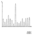
- This error sequence has a repeating progression, which implies that the spectrum of the output signal comprises the desired frequency as well as unwanted frequency components, so-called spuriuos components, which appear at distinct frequencies.
- a diagram of the spectrum (i.e. the relation between the frequency and the output power) of the output signal from such a DDS is illustrated in Fig. 1, from which it is apparent that the spurious components occur at distinct frequencies in the spectrum.
- a device for reducing unwanted spurious components in a DDS is previously known from US 5014231.
- random numbers are generated and added to the word in a reference table. In this manner, the spurious components are distributed randomly over the entire frequency spectrum.
- a device for reducing spurious components by introducing an "offset" in the frequency word supplied to an accumulator is previously known from US 4951237.
- a main object of the present invention is to provide an improved method and device in connection with a so-called direct digital synthesizer (DDS) in order to eliminate unwanted frequency components in the form of spurious components at distinct frequencies.
- DDS direct digital synthesizer
- the invention is based on the principle that a pseudo-random code is generated.
- the input code which corresponds to a desired frequency can be modulated.
- a code corresponding to said input code is regenerated in a calculation unit. The regeneration of the input code is carried out in a manner so that the pseudo-random code does not influence the desired frequency.
- the error sequence which is present in the output signal will not be of a periodical but instead of a random nature. In this manner, unwanted frequency components will be greatly reduced.
- Fig. 2 shows, in the form of a block diagram, a device according to the present invention.
- the device comprises a code generator 1 for generating a pseudo-random code P.
- the pseudocode P is subtracted from the frequency word F in a subtractor 3.
- the output signal F r1 from the adder 2 is supplied to the input of a first phase accumulator 4, whereas the output signal F r2 from the subtractor 3 is supplied to the input of a second phase accumulator 5.
- the output signal from the first phase accumulator 4 is supplied to a first reference table 6, i.e. a memory, which comprises a cosine wave as well as a sine wave, i.e. the cosine wave phase shifted 90°. These two curves can be regarded as the real part and the imaginary part, respectively, of the cosine wave.
- the output signals from the first reference table 6 are constituted by a real part cos 1 and an imaginary part sin 1 .
- the output signal from the second phase accumulator 5 is supplied to a second reference table 7 of a type which corresponds to the first reference table 6.
- the output signals from the second reference table 7 are constituted by a real part cos 2 and an imaginary part sin 2 .
- the desired frequency is obtained from a suitable selection of F.
- the output signal from the complex multiplying unit is supplied to a digital/analog converter 9 for generating an output analog wave shape.
- the pseudocode P does not influence the output frequency. Instead, it provides a random contribution to the frequency word F in the form of the words F r1 and F r2 .
- Fig. 3 shows a diagram of a spectrum (the output power as a function of the frequency) of the output signal according to the present invention.
- a problem is present in that the phase accumulator is repeatedly supplied with the same input data, which implies that the output signal is modulated with a periodical error sequence.
- the input data to the phase accumulators 4, 5 is changed each clock pulse due to the fact that the pseudo-random code P is used.
- the error sequence of the output signal is not periodical but instead has a random character, which is illustrated in Fig. 3.
- a noise component in the form of an equally distributed random number S can be inserted in the reference table 6.
Landscapes
- Engineering & Computer Science (AREA)
- Theoretical Computer Science (AREA)
- Physics & Mathematics (AREA)
- General Engineering & Computer Science (AREA)
- General Physics & Mathematics (AREA)
- Digital Transmission Methods That Use Modulated Carrier Waves (AREA)
- Amplitude Modulation (AREA)
Claims (5)
- Vorrichtung zum Reduzieren von unerwünschten Frequenzkomponenten bei einer digitalen Frequenzerzeugung, umfassend eine Akkumulatorvorrichtung (4, 5) zum Erzeugen von Ausgangssignalen in Abhängigkeit von einem Eingabecode (F) entsprechend einer erwünschten Frequenz, wobei die Akkumulatorvorrichtung (4, 5) mit mindestens einer Speichereinheit (6, 7) verbunden ist, die Codes in Entsprechung zu Wellenformen umfasst, und weiter einen Generator (1) zum Erzeugen eines Zufallscodes (P) umfassend,
dadurch gekennzeichnet, dass
diese eine Modulationseinheit (2, 3) umfasst, zum Erzeugen eines ersten modulierten Signals (Fr1), das die Summe des Eingabecodes (F) und des Zufallscodes (P) darstellt, und zum Erzeugen eines zweiten modulierten Signals (Fr2), das die Differenz zwischen dem Eingabecode (F) und dem Zufallscode (P) darstellt, wobei die Akkumulatorvorrichtung (4, 5) einen ersten Phasenakkumulator (4) umfasst, an den das erste modulierte Signal (Fr1) angelegt wird, und einen zweiten Phasenakkumulator (5), an den das zweite modulierte Signal (Fr2) angelegt wird, und eine Berechnungseinheit (8) zum regenerieren eines Codes entsprechend dem Eingabecode (F), durch Verknüpfen von Signalen bezüglich des ersten modulierten Signals (Fr1) und des zweiten modulierten Signals (Fr2), wobei die zu verknüpfenden Signale von der mindestens einen Speichereinheit (6,7) erhalten werden, auf eine Weise, so dass der Zufallscode (P) nicht die erwünschte Frequenz beeinflusst. - Vorrichtung nach Anspruch 1,
dadurch gekennzeichnet, dass
die Speichereinheit (6, 7) eine Cosinustabelle und eine Sinustabelle umfasst. - Vorrichtung nach einem der vorhergehenden Ansprüche,
dadurch gekennzeichnet, dass
die Berechnungseinheit (8) eine Einheit zur komplexen Multiplikation (8) umfasst, die nach der Speichereinheit (6, 7) angeordnet ist. - Verfahren zum Reduzieren von ungewollten Frequenzkomponenten bei einer digitalen Frequenzerzeugung, wobei ein Eingabecode (F) entsprechend einer gewünschten Frequenz erzeugt wird, und an eine Akkumulatorvorrichung (4, 5) geliefert wird, und ein Ausgabecode von der Akkumulatorvorrichtung (4, 5) an eine Speichereinheit (6, 7) geliefert wird, die Wellenformen entsprechende Codes,enthält, und wobei ein Zufallscode (P) erzeugt wird,
dadurch gekennzeichnet, dass
ein erstes Signal (Fr1), das die Summe des Eingabecodes (F) und des Zufallscodes (P) darstellt, und ein zweites Signal (Fr2), das die Differenz zwischen dem Eingabecode (F) und dem Zufallscode (P) darstellt, erzeugt wird, dass das erste und zweite Signal (Fr1, Fr2) an einen ersten Phasenakkumulator (4) bzw. einen zweiten Phasenakkumulator (5) geliefert werden, die einen Teil der Akkumulatorvorrichtung (4, 5) bilden, und dass der Eingabecode (F) aus dem Signal regeneriert wird, das von der Speichereinheit (6, 7) geliefert wird, indem Signale in Zusammenhang mit dem ersten Signal (Fr1) und dem zweiten Signal (Fr2) verknüpft werden, wobei die zu verknüpfenden Signale von der mindestens einen Speichereinheit (6, 7) auf solche Weise erhalten werden, dass der Zufallscode (P) nicht die erwünschte Frequenz beeinflusst. - Verfahren nach Anspruch 4,
dadurch gekennzeichnet, dass
der Eingabecode (F) mittels einer komplexen Multiplikation von Signalen regeneriert wird, die von der Speichereinheit (6, 7) geliefert werden.
Applications Claiming Priority (2)
| Application Number | Priority Date | Filing Date | Title |
|---|---|---|---|
| SE9404311 | 1994-12-12 | ||
| SE9404311A SE506694C2 (sv) | 1994-12-12 | 1994-12-12 | Anordning och förfarande för reducering av oönskade frekvenskomponenter vid digital frekvensgenerering |
Publications (2)
| Publication Number | Publication Date |
|---|---|
| EP0717340A1 EP0717340A1 (de) | 1996-06-19 |
| EP0717340B1 true EP0717340B1 (de) | 2002-03-20 |
Family
ID=20396297
Family Applications (1)
| Application Number | Title | Priority Date | Filing Date |
|---|---|---|---|
| EP95850215A Expired - Lifetime EP0717340B1 (de) | 1994-12-12 | 1995-12-05 | Einrichtung und Verfahren zur Frequenzerzeugung |
Country Status (4)
| Country | Link |
|---|---|
| US (1) | US5761101A (de) |
| EP (1) | EP0717340B1 (de) |
| DE (1) | DE69525909T2 (de) |
| SE (1) | SE506694C2 (de) |
Families Citing this family (5)
| Publication number | Priority date | Publication date | Assignee | Title |
|---|---|---|---|---|
| US6748408B1 (en) * | 1999-10-21 | 2004-06-08 | International Buisness Machines Corporation | Programmable non-integer fractional divider |
| US6587863B1 (en) * | 2000-06-27 | 2003-07-01 | Analog Devices, Inc. | Multiphase, interleaved direct digital synthesis methods and structures |
| US6779849B1 (en) * | 2001-04-24 | 2004-08-24 | The Lane Company, Inc. | Multi-channel sling seat frame |
| GB2449461A (en) * | 2007-05-23 | 2008-11-26 | Agilent Technologies Inc | Noise reduction in direct digital synthesis signal mixer by injecting then cancelling a pseudo noise component in the carrier wave |
| US20100194444A1 (en) * | 2009-01-30 | 2010-08-05 | Agilent Technolgies, Inc | Reduction of spurious frequency components in direct digital synthesis |
Family Cites Families (6)
| Publication number | Priority date | Publication date | Assignee | Title |
|---|---|---|---|---|
| US4890248A (en) * | 1987-06-01 | 1989-12-26 | Hughes Aircraft Company | Method and apparatus for reducing aliasing in signal processing |
| US5014231A (en) * | 1987-11-23 | 1991-05-07 | Hughes Aircraft Company | Randomized digital/analog converter direct digital synthesizer |
| US4901265A (en) * | 1987-12-14 | 1990-02-13 | Qualcomm, Inc. | Pseudorandom dither for frequency synthesis noise |
| US4951237A (en) * | 1988-04-22 | 1990-08-21 | Hughes Aircraft Company | Direct digital synthesizer with selectably randomized accumulator |
| JPH0763124B2 (ja) * | 1993-02-24 | 1995-07-05 | 日本電気株式会社 | 直接デジタル周波数シンセサイザ |
| US5291428A (en) * | 1993-03-02 | 1994-03-01 | Harris Corporation | Apparatus for reducing spurious frequency components in the output signal of a direct digital synthesizer |
-
1994
- 1994-12-12 SE SE9404311A patent/SE506694C2/sv not_active IP Right Cessation
-
1995
- 1995-12-05 EP EP95850215A patent/EP0717340B1/de not_active Expired - Lifetime
- 1995-12-05 DE DE69525909T patent/DE69525909T2/de not_active Expired - Lifetime
- 1995-12-11 US US08/570,513 patent/US5761101A/en not_active Expired - Lifetime
Also Published As
| Publication number | Publication date |
|---|---|
| US5761101A (en) | 1998-06-02 |
| SE9404311L (sv) | 1996-06-13 |
| SE9404311D0 (sv) | 1994-12-12 |
| EP0717340A1 (de) | 1996-06-19 |
| DE69525909D1 (de) | 2002-04-25 |
| DE69525909T2 (de) | 2002-11-07 |
| SE506694C2 (sv) | 1998-02-02 |
Similar Documents
| Publication | Publication Date | Title |
|---|---|---|
| US5563535A (en) | Direct digital frequency synthesizer using sigma-delta techniques | |
| JP2823913B2 (ja) | 周波数合成雑音に対する疑似ランダム振動 | |
| KR0130471B1 (ko) | Ssb 신호 발생기 | |
| JP2659022B2 (ja) | 選択可能なランダム化したアキュムレータを有する直接デジタルシンセサイザ | |
| JP3410355B2 (ja) | 変調器及び変調方法 | |
| EP0935339B1 (de) | Vielseitiger Signalgenerator | |
| WO2004092935A1 (en) | Direct digital frequency synthesizer for cellular wireless communication systems based on fast frequency-hopped spread spectrum technology | |
| US6281823B1 (en) | Direct digital synthesis using a sine weighted DAC | |
| US5986483A (en) | Direct digital frequency systhesizer | |
| US20020150169A1 (en) | Apparatus and method for measuring propagation delay in an NB-TDD CDMA mobile communication system | |
| US6347325B1 (en) | Direct-digital synthesizers | |
| WO1995006990A1 (en) | Direct digital frequency synthesizer | |
| EP1103125B1 (de) | Digital gesteuerter Oszillator mit einer größenreduzierten Nachschlagetabelle und dazugehöriges Verfahren | |
| US5761101A (en) | Device and method for frequency generation | |
| US5864492A (en) | Randomized digital waveshape samples from a look up table | |
| WO2001007992A1 (en) | Method and system for generating a trigonometric function | |
| US5424664A (en) | Direct digital synthesizer with adjustable clock frequency | |
| US5382924A (en) | Continuous phase frequency shift keying modulator | |
| KR960706710A (ko) | 협대역 임의적 hf 변조 및 노이즈 발생기(narrow band, arbitrary hf modulation and noise generator) | |
| JPS6387808A (ja) | チヤ−プ信号発生回路 | |
| JP3888154B2 (ja) | 変調信号発生装置 | |
| JP2905503B2 (ja) | ディジタル式クロック発生装置 | |
| US7583638B2 (en) | Device and method for processing a digital data signal in a CDMA radio transmitter | |
| Schnoll | Direct Digital Synthesis Techniques to Improve Oscillator Phase Noise and Spurious Content | |
| KR100295099B1 (ko) | 삼각함수계산을이용한직접디지털주파수합성장치 |
Legal Events
| Date | Code | Title | Description |
|---|---|---|---|
| PUAI | Public reference made under article 153(3) epc to a published international application that has entered the european phase |
Free format text: ORIGINAL CODE: 0009012 |
|
| AK | Designated contracting states |
Kind code of ref document: A1 Designated state(s): DE FR GB NL |
|
| 17P | Request for examination filed |
Effective date: 19961205 |
|
| 17Q | First examination report despatched |
Effective date: 19991216 |
|
| GRAG | Despatch of communication of intention to grant |
Free format text: ORIGINAL CODE: EPIDOS AGRA |
|
| GRAG | Despatch of communication of intention to grant |
Free format text: ORIGINAL CODE: EPIDOS AGRA |
|
| GRAH | Despatch of communication of intention to grant a patent |
Free format text: ORIGINAL CODE: EPIDOS IGRA |
|
| GRAH | Despatch of communication of intention to grant a patent |
Free format text: ORIGINAL CODE: EPIDOS IGRA |
|
| REG | Reference to a national code |
Ref country code: GB Ref legal event code: IF02 |
|
| GRAA | (expected) grant |
Free format text: ORIGINAL CODE: 0009210 |
|
| AK | Designated contracting states |
Kind code of ref document: B1 Designated state(s): DE FR GB NL |
|
| REF | Corresponds to: |
Ref document number: 69525909 Country of ref document: DE Date of ref document: 20020425 |
|
| ET | Fr: translation filed | ||
| ET | Fr: translation filed | ||
| PLBE | No opposition filed within time limit |
Free format text: ORIGINAL CODE: 0009261 |
|
| STAA | Information on the status of an ep patent application or granted ep patent |
Free format text: STATUS: NO OPPOSITION FILED WITHIN TIME LIMIT |
|
| 26N | No opposition filed |
Effective date: 20021223 |
|
| PGFP | Annual fee paid to national office [announced via postgrant information from national office to epo] |
Ref country code: GB Payment date: 20141229 Year of fee payment: 20 |
|
| PGFP | Annual fee paid to national office [announced via postgrant information from national office to epo] |
Ref country code: NL Payment date: 20141226 Year of fee payment: 20 Ref country code: FR Payment date: 20141217 Year of fee payment: 20 |
|
| PGFP | Annual fee paid to national office [announced via postgrant information from national office to epo] |
Ref country code: DE Payment date: 20141230 Year of fee payment: 20 |
|
| REG | Reference to a national code |
Ref country code: DE Ref legal event code: R071 Ref document number: 69525909 Country of ref document: DE |
|
| REG | Reference to a national code |
Ref country code: NL Ref legal event code: MK Effective date: 20151204 |
|
| REG | Reference to a national code |
Ref country code: GB Ref legal event code: PE20 Expiry date: 20151204 |
|
| PG25 | Lapsed in a contracting state [announced via postgrant information from national office to epo] |
Ref country code: GB Free format text: LAPSE BECAUSE OF EXPIRATION OF PROTECTION Effective date: 20151204 |