EP0706208A2 - Halbleiterpackung integral mit Halbleiterchip und Herstellungsverfahren dafür - Google Patents
Halbleiterpackung integral mit Halbleiterchip und Herstellungsverfahren dafür Download PDFInfo
- Publication number
- EP0706208A2 EP0706208A2 EP95115550A EP95115550A EP0706208A2 EP 0706208 A2 EP0706208 A2 EP 0706208A2 EP 95115550 A EP95115550 A EP 95115550A EP 95115550 A EP95115550 A EP 95115550A EP 0706208 A2 EP0706208 A2 EP 0706208A2
- Authority
- EP
- European Patent Office
- Prior art keywords
- passivating film
- semiconductor
- semiconductor package
- contacts
- holes
- Prior art date
- Legal status (The legal status is an assumption and is not a legal conclusion. Google has not performed a legal analysis and makes no representation as to the accuracy of the status listed.)
- Granted
Links
Images


Classifications
-
- H—ELECTRICITY
- H01—ELECTRIC ELEMENTS
- H01L—SEMICONDUCTOR DEVICES NOT COVERED BY CLASS H10
- H01L24/00—Arrangements for connecting or disconnecting semiconductor or solid-state bodies; Methods or apparatus related thereto
- H01L24/80—Methods for connecting semiconductor or other solid state bodies using means for bonding being attached to, or being formed on, the surface to be connected
- H01L24/81—Methods for connecting semiconductor or other solid state bodies using means for bonding being attached to, or being formed on, the surface to be connected using a bump connector
-
- H—ELECTRICITY
- H01—ELECTRIC ELEMENTS
- H01L—SEMICONDUCTOR DEVICES NOT COVERED BY CLASS H10
- H01L23/00—Details of semiconductor or other solid state devices
- H01L23/02—Containers; Seals
- H01L23/04—Containers; Seals characterised by the shape of the container or parts, e.g. caps, walls
-
- H—ELECTRICITY
- H01—ELECTRIC ELEMENTS
- H01L—SEMICONDUCTOR DEVICES NOT COVERED BY CLASS H10
- H01L23/00—Details of semiconductor or other solid state devices
- H01L23/28—Encapsulations, e.g. encapsulating layers, coatings, e.g. for protection
- H01L23/31—Encapsulations, e.g. encapsulating layers, coatings, e.g. for protection characterised by the arrangement or shape
- H01L23/3157—Partial encapsulation or coating
- H01L23/3171—Partial encapsulation or coating the coating being directly applied to the semiconductor body, e.g. passivation layer
-
- H—ELECTRICITY
- H01—ELECTRIC ELEMENTS
- H01L—SEMICONDUCTOR DEVICES NOT COVERED BY CLASS H10
- H01L23/00—Details of semiconductor or other solid state devices
- H01L23/52—Arrangements for conducting electric current within the device in operation from one component to another, i.e. interconnections, e.g. wires, lead frames
- H01L23/522—Arrangements for conducting electric current within the device in operation from one component to another, i.e. interconnections, e.g. wires, lead frames including external interconnections consisting of a multilayer structure of conductive and insulating layers inseparably formed on the semiconductor body
- H01L23/525—Arrangements for conducting electric current within the device in operation from one component to another, i.e. interconnections, e.g. wires, lead frames including external interconnections consisting of a multilayer structure of conductive and insulating layers inseparably formed on the semiconductor body with adaptable interconnections
-
- H—ELECTRICITY
- H01—ELECTRIC ELEMENTS
- H01L—SEMICONDUCTOR DEVICES NOT COVERED BY CLASS H10
- H01L23/00—Details of semiconductor or other solid state devices
- H01L23/52—Arrangements for conducting electric current within the device in operation from one component to another, i.e. interconnections, e.g. wires, lead frames
- H01L23/522—Arrangements for conducting electric current within the device in operation from one component to another, i.e. interconnections, e.g. wires, lead frames including external interconnections consisting of a multilayer structure of conductive and insulating layers inseparably formed on the semiconductor body
- H01L23/528—Geometry or layout of the interconnection structure
- H01L23/5283—Cross-sectional geometry
-
- H—ELECTRICITY
- H01—ELECTRIC ELEMENTS
- H01L—SEMICONDUCTOR DEVICES NOT COVERED BY CLASS H10
- H01L24/00—Arrangements for connecting or disconnecting semiconductor or solid-state bodies; Methods or apparatus related thereto
- H01L24/01—Means for bonding being attached to, or being formed on, the surface to be connected, e.g. chip-to-package, die-attach, "first-level" interconnects; Manufacturing methods related thereto
- H01L24/02—Bonding areas ; Manufacturing methods related thereto
- H01L24/04—Structure, shape, material or disposition of the bonding areas prior to the connecting process
- H01L24/05—Structure, shape, material or disposition of the bonding areas prior to the connecting process of an individual bonding area
-
- H—ELECTRICITY
- H01—ELECTRIC ELEMENTS
- H01L—SEMICONDUCTOR DEVICES NOT COVERED BY CLASS H10
- H01L2224/00—Indexing scheme for arrangements for connecting or disconnecting semiconductor or solid-state bodies and methods related thereto as covered by H01L24/00
- H01L2224/01—Means for bonding being attached to, or being formed on, the surface to be connected, e.g. chip-to-package, die-attach, "first-level" interconnects; Manufacturing methods related thereto
- H01L2224/02—Bonding areas; Manufacturing methods related thereto
- H01L2224/023—Redistribution layers [RDL] for bonding areas
- H01L2224/0237—Disposition of the redistribution layers
- H01L2224/02377—Fan-in arrangement
-
- H—ELECTRICITY
- H01—ELECTRIC ELEMENTS
- H01L—SEMICONDUCTOR DEVICES NOT COVERED BY CLASS H10
- H01L2224/00—Indexing scheme for arrangements for connecting or disconnecting semiconductor or solid-state bodies and methods related thereto as covered by H01L24/00
- H01L2224/01—Means for bonding being attached to, or being formed on, the surface to be connected, e.g. chip-to-package, die-attach, "first-level" interconnects; Manufacturing methods related thereto
- H01L2224/02—Bonding areas; Manufacturing methods related thereto
- H01L2224/04—Structure, shape, material or disposition of the bonding areas prior to the connecting process
- H01L2224/0401—Bonding areas specifically adapted for bump connectors, e.g. under bump metallisation [UBM]
-
- H—ELECTRICITY
- H01—ELECTRIC ELEMENTS
- H01L—SEMICONDUCTOR DEVICES NOT COVERED BY CLASS H10
- H01L2224/00—Indexing scheme for arrangements for connecting or disconnecting semiconductor or solid-state bodies and methods related thereto as covered by H01L24/00
- H01L2224/01—Means for bonding being attached to, or being formed on, the surface to be connected, e.g. chip-to-package, die-attach, "first-level" interconnects; Manufacturing methods related thereto
- H01L2224/02—Bonding areas; Manufacturing methods related thereto
- H01L2224/04—Structure, shape, material or disposition of the bonding areas prior to the connecting process
- H01L2224/04105—Bonding areas formed on an encapsulation of the semiconductor or solid-state body, e.g. bonding areas on chip-scale packages
-
- H—ELECTRICITY
- H01—ELECTRIC ELEMENTS
- H01L—SEMICONDUCTOR DEVICES NOT COVERED BY CLASS H10
- H01L2224/00—Indexing scheme for arrangements for connecting or disconnecting semiconductor or solid-state bodies and methods related thereto as covered by H01L24/00
- H01L2224/01—Means for bonding being attached to, or being formed on, the surface to be connected, e.g. chip-to-package, die-attach, "first-level" interconnects; Manufacturing methods related thereto
- H01L2224/02—Bonding areas; Manufacturing methods related thereto
- H01L2224/04—Structure, shape, material or disposition of the bonding areas prior to the connecting process
- H01L2224/05—Structure, shape, material or disposition of the bonding areas prior to the connecting process of an individual bonding area
- H01L2224/05001—Internal layers
- H01L2224/05099—Material
- H01L2224/051—Material with a principal constituent of the material being a metal or a metalloid, e.g. boron [B], silicon [Si], germanium [Ge], arsenic [As], antimony [Sb], tellurium [Te] and polonium [Po], and alloys thereof
- H01L2224/05117—Material with a principal constituent of the material being a metal or a metalloid, e.g. boron [B], silicon [Si], germanium [Ge], arsenic [As], antimony [Sb], tellurium [Te] and polonium [Po], and alloys thereof the principal constituent melting at a temperature of greater than or equal to 400°C and less than 950°C
- H01L2224/05124—Aluminium [Al] as principal constituent
-
- H—ELECTRICITY
- H01—ELECTRIC ELEMENTS
- H01L—SEMICONDUCTOR DEVICES NOT COVERED BY CLASS H10
- H01L2224/00—Indexing scheme for arrangements for connecting or disconnecting semiconductor or solid-state bodies and methods related thereto as covered by H01L24/00
- H01L2224/01—Means for bonding being attached to, or being formed on, the surface to be connected, e.g. chip-to-package, die-attach, "first-level" interconnects; Manufacturing methods related thereto
- H01L2224/02—Bonding areas; Manufacturing methods related thereto
- H01L2224/04—Structure, shape, material or disposition of the bonding areas prior to the connecting process
- H01L2224/05—Structure, shape, material or disposition of the bonding areas prior to the connecting process of an individual bonding area
- H01L2224/05001—Internal layers
- H01L2224/05099—Material
- H01L2224/051—Material with a principal constituent of the material being a metal or a metalloid, e.g. boron [B], silicon [Si], germanium [Ge], arsenic [As], antimony [Sb], tellurium [Te] and polonium [Po], and alloys thereof
- H01L2224/05138—Material with a principal constituent of the material being a metal or a metalloid, e.g. boron [B], silicon [Si], germanium [Ge], arsenic [As], antimony [Sb], tellurium [Te] and polonium [Po], and alloys thereof the principal constituent melting at a temperature of greater than or equal to 950°C and less than 1550°C
- H01L2224/05147—Copper [Cu] as principal constituent
-
- H—ELECTRICITY
- H01—ELECTRIC ELEMENTS
- H01L—SEMICONDUCTOR DEVICES NOT COVERED BY CLASS H10
- H01L2224/00—Indexing scheme for arrangements for connecting or disconnecting semiconductor or solid-state bodies and methods related thereto as covered by H01L24/00
- H01L2224/01—Means for bonding being attached to, or being formed on, the surface to be connected, e.g. chip-to-package, die-attach, "first-level" interconnects; Manufacturing methods related thereto
- H01L2224/02—Bonding areas; Manufacturing methods related thereto
- H01L2224/04—Structure, shape, material or disposition of the bonding areas prior to the connecting process
- H01L2224/05—Structure, shape, material or disposition of the bonding areas prior to the connecting process of an individual bonding area
- H01L2224/05001—Internal layers
- H01L2224/05099—Material
- H01L2224/051—Material with a principal constituent of the material being a metal or a metalloid, e.g. boron [B], silicon [Si], germanium [Ge], arsenic [As], antimony [Sb], tellurium [Te] and polonium [Po], and alloys thereof
- H01L2224/05138—Material with a principal constituent of the material being a metal or a metalloid, e.g. boron [B], silicon [Si], germanium [Ge], arsenic [As], antimony [Sb], tellurium [Te] and polonium [Po], and alloys thereof the principal constituent melting at a temperature of greater than or equal to 950°C and less than 1550°C
- H01L2224/05155—Nickel [Ni] as principal constituent
-
- H—ELECTRICITY
- H01—ELECTRIC ELEMENTS
- H01L—SEMICONDUCTOR DEVICES NOT COVERED BY CLASS H10
- H01L2224/00—Indexing scheme for arrangements for connecting or disconnecting semiconductor or solid-state bodies and methods related thereto as covered by H01L24/00
- H01L2224/01—Means for bonding being attached to, or being formed on, the surface to be connected, e.g. chip-to-package, die-attach, "first-level" interconnects; Manufacturing methods related thereto
- H01L2224/02—Bonding areas; Manufacturing methods related thereto
- H01L2224/04—Structure, shape, material or disposition of the bonding areas prior to the connecting process
- H01L2224/05—Structure, shape, material or disposition of the bonding areas prior to the connecting process of an individual bonding area
- H01L2224/05001—Internal layers
- H01L2224/05099—Material
- H01L2224/051—Material with a principal constituent of the material being a metal or a metalloid, e.g. boron [B], silicon [Si], germanium [Ge], arsenic [As], antimony [Sb], tellurium [Te] and polonium [Po], and alloys thereof
- H01L2224/05163—Material with a principal constituent of the material being a metal or a metalloid, e.g. boron [B], silicon [Si], germanium [Ge], arsenic [As], antimony [Sb], tellurium [Te] and polonium [Po], and alloys thereof the principal constituent melting at a temperature of greater than 1550°C
- H01L2224/05164—Palladium [Pd] as principal constituent
-
- H—ELECTRICITY
- H01—ELECTRIC ELEMENTS
- H01L—SEMICONDUCTOR DEVICES NOT COVERED BY CLASS H10
- H01L2224/00—Indexing scheme for arrangements for connecting or disconnecting semiconductor or solid-state bodies and methods related thereto as covered by H01L24/00
- H01L2224/01—Means for bonding being attached to, or being formed on, the surface to be connected, e.g. chip-to-package, die-attach, "first-level" interconnects; Manufacturing methods related thereto
- H01L2224/02—Bonding areas; Manufacturing methods related thereto
- H01L2224/04—Structure, shape, material or disposition of the bonding areas prior to the connecting process
- H01L2224/05—Structure, shape, material or disposition of the bonding areas prior to the connecting process of an individual bonding area
- H01L2224/05001—Internal layers
- H01L2224/05099—Material
- H01L2224/051—Material with a principal constituent of the material being a metal or a metalloid, e.g. boron [B], silicon [Si], germanium [Ge], arsenic [As], antimony [Sb], tellurium [Te] and polonium [Po], and alloys thereof
- H01L2224/05163—Material with a principal constituent of the material being a metal or a metalloid, e.g. boron [B], silicon [Si], germanium [Ge], arsenic [As], antimony [Sb], tellurium [Te] and polonium [Po], and alloys thereof the principal constituent melting at a temperature of greater than 1550°C
- H01L2224/05166—Titanium [Ti] as principal constituent
-
- H—ELECTRICITY
- H01—ELECTRIC ELEMENTS
- H01L—SEMICONDUCTOR DEVICES NOT COVERED BY CLASS H10
- H01L2224/00—Indexing scheme for arrangements for connecting or disconnecting semiconductor or solid-state bodies and methods related thereto as covered by H01L24/00
- H01L2224/01—Means for bonding being attached to, or being formed on, the surface to be connected, e.g. chip-to-package, die-attach, "first-level" interconnects; Manufacturing methods related thereto
- H01L2224/02—Bonding areas; Manufacturing methods related thereto
- H01L2224/04—Structure, shape, material or disposition of the bonding areas prior to the connecting process
- H01L2224/05—Structure, shape, material or disposition of the bonding areas prior to the connecting process of an individual bonding area
- H01L2224/0554—External layer
- H01L2224/0555—Shape
- H01L2224/05552—Shape in top view
- H01L2224/05554—Shape in top view being square
-
- H—ELECTRICITY
- H01—ELECTRIC ELEMENTS
- H01L—SEMICONDUCTOR DEVICES NOT COVERED BY CLASS H10
- H01L2224/00—Indexing scheme for arrangements for connecting or disconnecting semiconductor or solid-state bodies and methods related thereto as covered by H01L24/00
- H01L2224/01—Means for bonding being attached to, or being formed on, the surface to be connected, e.g. chip-to-package, die-attach, "first-level" interconnects; Manufacturing methods related thereto
- H01L2224/02—Bonding areas; Manufacturing methods related thereto
- H01L2224/04—Structure, shape, material or disposition of the bonding areas prior to the connecting process
- H01L2224/05—Structure, shape, material or disposition of the bonding areas prior to the connecting process of an individual bonding area
- H01L2224/0554—External layer
- H01L2224/0555—Shape
- H01L2224/05556—Shape in side view
- H01L2224/05559—Shape in side view non conformal layer on a patterned surface
-
- H—ELECTRICITY
- H01—ELECTRIC ELEMENTS
- H01L—SEMICONDUCTOR DEVICES NOT COVERED BY CLASS H10
- H01L2224/00—Indexing scheme for arrangements for connecting or disconnecting semiconductor or solid-state bodies and methods related thereto as covered by H01L24/00
- H01L2224/01—Means for bonding being attached to, or being formed on, the surface to be connected, e.g. chip-to-package, die-attach, "first-level" interconnects; Manufacturing methods related thereto
- H01L2224/02—Bonding areas; Manufacturing methods related thereto
- H01L2224/04—Structure, shape, material or disposition of the bonding areas prior to the connecting process
- H01L2224/05—Structure, shape, material or disposition of the bonding areas prior to the connecting process of an individual bonding area
- H01L2224/0554—External layer
- H01L2224/0556—Disposition
- H01L2224/05571—Disposition the external layer being disposed in a recess of the surface
- H01L2224/05572—Disposition the external layer being disposed in a recess of the surface the external layer extending out of an opening
-
- H—ELECTRICITY
- H01—ELECTRIC ELEMENTS
- H01L—SEMICONDUCTOR DEVICES NOT COVERED BY CLASS H10
- H01L2224/00—Indexing scheme for arrangements for connecting or disconnecting semiconductor or solid-state bodies and methods related thereto as covered by H01L24/00
- H01L2224/01—Means for bonding being attached to, or being formed on, the surface to be connected, e.g. chip-to-package, die-attach, "first-level" interconnects; Manufacturing methods related thereto
- H01L2224/02—Bonding areas; Manufacturing methods related thereto
- H01L2224/04—Structure, shape, material or disposition of the bonding areas prior to the connecting process
- H01L2224/05—Structure, shape, material or disposition of the bonding areas prior to the connecting process of an individual bonding area
- H01L2224/0554—External layer
- H01L2224/05599—Material
- H01L2224/056—Material with a principal constituent of the material being a metal or a metalloid, e.g. boron [B], silicon [Si], germanium [Ge], arsenic [As], antimony [Sb], tellurium [Te] and polonium [Po], and alloys thereof
- H01L2224/05638—Material with a principal constituent of the material being a metal or a metalloid, e.g. boron [B], silicon [Si], germanium [Ge], arsenic [As], antimony [Sb], tellurium [Te] and polonium [Po], and alloys thereof the principal constituent melting at a temperature of greater than or equal to 950°C and less than 1550°C
- H01L2224/05644—Gold [Au] as principal constituent
-
- H—ELECTRICITY
- H01—ELECTRIC ELEMENTS
- H01L—SEMICONDUCTOR DEVICES NOT COVERED BY CLASS H10
- H01L2224/00—Indexing scheme for arrangements for connecting or disconnecting semiconductor or solid-state bodies and methods related thereto as covered by H01L24/00
- H01L2224/01—Means for bonding being attached to, or being formed on, the surface to be connected, e.g. chip-to-package, die-attach, "first-level" interconnects; Manufacturing methods related thereto
- H01L2224/02—Bonding areas; Manufacturing methods related thereto
- H01L2224/04—Structure, shape, material or disposition of the bonding areas prior to the connecting process
- H01L2224/05—Structure, shape, material or disposition of the bonding areas prior to the connecting process of an individual bonding area
- H01L2224/0554—External layer
- H01L2224/05599—Material
- H01L2224/056—Material with a principal constituent of the material being a metal or a metalloid, e.g. boron [B], silicon [Si], germanium [Ge], arsenic [As], antimony [Sb], tellurium [Te] and polonium [Po], and alloys thereof
- H01L2224/05638—Material with a principal constituent of the material being a metal or a metalloid, e.g. boron [B], silicon [Si], germanium [Ge], arsenic [As], antimony [Sb], tellurium [Te] and polonium [Po], and alloys thereof the principal constituent melting at a temperature of greater than or equal to 950°C and less than 1550°C
- H01L2224/05647—Copper [Cu] as principal constituent
-
- H—ELECTRICITY
- H01—ELECTRIC ELEMENTS
- H01L—SEMICONDUCTOR DEVICES NOT COVERED BY CLASS H10
- H01L2224/00—Indexing scheme for arrangements for connecting or disconnecting semiconductor or solid-state bodies and methods related thereto as covered by H01L24/00
- H01L2224/01—Means for bonding being attached to, or being formed on, the surface to be connected, e.g. chip-to-package, die-attach, "first-level" interconnects; Manufacturing methods related thereto
- H01L2224/02—Bonding areas; Manufacturing methods related thereto
- H01L2224/04—Structure, shape, material or disposition of the bonding areas prior to the connecting process
- H01L2224/05—Structure, shape, material or disposition of the bonding areas prior to the connecting process of an individual bonding area
- H01L2224/0554—External layer
- H01L2224/05599—Material
- H01L2224/056—Material with a principal constituent of the material being a metal or a metalloid, e.g. boron [B], silicon [Si], germanium [Ge], arsenic [As], antimony [Sb], tellurium [Te] and polonium [Po], and alloys thereof
- H01L2224/05638—Material with a principal constituent of the material being a metal or a metalloid, e.g. boron [B], silicon [Si], germanium [Ge], arsenic [As], antimony [Sb], tellurium [Te] and polonium [Po], and alloys thereof the principal constituent melting at a temperature of greater than or equal to 950°C and less than 1550°C
- H01L2224/05655—Nickel [Ni] as principal constituent
-
- H—ELECTRICITY
- H01—ELECTRIC ELEMENTS
- H01L—SEMICONDUCTOR DEVICES NOT COVERED BY CLASS H10
- H01L2224/00—Indexing scheme for arrangements for connecting or disconnecting semiconductor or solid-state bodies and methods related thereto as covered by H01L24/00
- H01L2224/01—Means for bonding being attached to, or being formed on, the surface to be connected, e.g. chip-to-package, die-attach, "first-level" interconnects; Manufacturing methods related thereto
- H01L2224/02—Bonding areas; Manufacturing methods related thereto
- H01L2224/04—Structure, shape, material or disposition of the bonding areas prior to the connecting process
- H01L2224/06—Structure, shape, material or disposition of the bonding areas prior to the connecting process of a plurality of bonding areas
- H01L2224/061—Disposition
- H01L2224/0612—Layout
- H01L2224/0613—Square or rectangular array
- H01L2224/06131—Square or rectangular array being uniform, i.e. having a uniform pitch across the array
-
- H—ELECTRICITY
- H01—ELECTRIC ELEMENTS
- H01L—SEMICONDUCTOR DEVICES NOT COVERED BY CLASS H10
- H01L2224/00—Indexing scheme for arrangements for connecting or disconnecting semiconductor or solid-state bodies and methods related thereto as covered by H01L24/00
- H01L2224/01—Means for bonding being attached to, or being formed on, the surface to be connected, e.g. chip-to-package, die-attach, "first-level" interconnects; Manufacturing methods related thereto
- H01L2224/10—Bump connectors; Manufacturing methods related thereto
- H01L2224/11—Manufacturing methods
- H01L2224/1147—Manufacturing methods using a lift-off mask
-
- H—ELECTRICITY
- H01—ELECTRIC ELEMENTS
- H01L—SEMICONDUCTOR DEVICES NOT COVERED BY CLASS H10
- H01L2224/00—Indexing scheme for arrangements for connecting or disconnecting semiconductor or solid-state bodies and methods related thereto as covered by H01L24/00
- H01L2224/01—Means for bonding being attached to, or being formed on, the surface to be connected, e.g. chip-to-package, die-attach, "first-level" interconnects; Manufacturing methods related thereto
- H01L2224/10—Bump connectors; Manufacturing methods related thereto
- H01L2224/12—Structure, shape, material or disposition of the bump connectors prior to the connecting process
- H01L2224/12105—Bump connectors formed on an encapsulation of the semiconductor or solid-state body, e.g. bumps on chip-scale packages
-
- H—ELECTRICITY
- H01—ELECTRIC ELEMENTS
- H01L—SEMICONDUCTOR DEVICES NOT COVERED BY CLASS H10
- H01L2224/00—Indexing scheme for arrangements for connecting or disconnecting semiconductor or solid-state bodies and methods related thereto as covered by H01L24/00
- H01L2224/01—Means for bonding being attached to, or being formed on, the surface to be connected, e.g. chip-to-package, die-attach, "first-level" interconnects; Manufacturing methods related thereto
- H01L2224/10—Bump connectors; Manufacturing methods related thereto
- H01L2224/12—Structure, shape, material or disposition of the bump connectors prior to the connecting process
- H01L2224/13—Structure, shape, material or disposition of the bump connectors prior to the connecting process of an individual bump connector
- H01L2224/13001—Core members of the bump connector
- H01L2224/13005—Structure
- H01L2224/13007—Bump connector smaller than the underlying bonding area, e.g. than the under bump metallisation [UBM]
-
- H—ELECTRICITY
- H01—ELECTRIC ELEMENTS
- H01L—SEMICONDUCTOR DEVICES NOT COVERED BY CLASS H10
- H01L2224/00—Indexing scheme for arrangements for connecting or disconnecting semiconductor or solid-state bodies and methods related thereto as covered by H01L24/00
- H01L2224/01—Means for bonding being attached to, or being formed on, the surface to be connected, e.g. chip-to-package, die-attach, "first-level" interconnects; Manufacturing methods related thereto
- H01L2224/10—Bump connectors; Manufacturing methods related thereto
- H01L2224/12—Structure, shape, material or disposition of the bump connectors prior to the connecting process
- H01L2224/13—Structure, shape, material or disposition of the bump connectors prior to the connecting process of an individual bump connector
- H01L2224/13001—Core members of the bump connector
- H01L2224/1302—Disposition
- H01L2224/13023—Disposition the whole bump connector protruding from the surface
-
- H—ELECTRICITY
- H01—ELECTRIC ELEMENTS
- H01L—SEMICONDUCTOR DEVICES NOT COVERED BY CLASS H10
- H01L2224/00—Indexing scheme for arrangements for connecting or disconnecting semiconductor or solid-state bodies and methods related thereto as covered by H01L24/00
- H01L2224/01—Means for bonding being attached to, or being formed on, the surface to be connected, e.g. chip-to-package, die-attach, "first-level" interconnects; Manufacturing methods related thereto
- H01L2224/10—Bump connectors; Manufacturing methods related thereto
- H01L2224/12—Structure, shape, material or disposition of the bump connectors prior to the connecting process
- H01L2224/13—Structure, shape, material or disposition of the bump connectors prior to the connecting process of an individual bump connector
- H01L2224/13001—Core members of the bump connector
- H01L2224/13099—Material
-
- H—ELECTRICITY
- H01—ELECTRIC ELEMENTS
- H01L—SEMICONDUCTOR DEVICES NOT COVERED BY CLASS H10
- H01L2224/00—Indexing scheme for arrangements for connecting or disconnecting semiconductor or solid-state bodies and methods related thereto as covered by H01L24/00
- H01L2224/01—Means for bonding being attached to, or being formed on, the surface to be connected, e.g. chip-to-package, die-attach, "first-level" interconnects; Manufacturing methods related thereto
- H01L2224/10—Bump connectors; Manufacturing methods related thereto
- H01L2224/12—Structure, shape, material or disposition of the bump connectors prior to the connecting process
- H01L2224/14—Structure, shape, material or disposition of the bump connectors prior to the connecting process of a plurality of bump connectors
- H01L2224/141—Disposition
- H01L2224/1412—Layout
- H01L2224/1413—Square or rectangular array
- H01L2224/14134—Square or rectangular array covering only portions of the surface to be connected
-
- H—ELECTRICITY
- H01—ELECTRIC ELEMENTS
- H01L—SEMICONDUCTOR DEVICES NOT COVERED BY CLASS H10
- H01L2224/00—Indexing scheme for arrangements for connecting or disconnecting semiconductor or solid-state bodies and methods related thereto as covered by H01L24/00
- H01L2224/80—Methods for connecting semiconductor or other solid state bodies using means for bonding being attached to, or being formed on, the surface to be connected
- H01L2224/81—Methods for connecting semiconductor or other solid state bodies using means for bonding being attached to, or being formed on, the surface to be connected using a bump connector
- H01L2224/818—Bonding techniques
- H01L2224/81801—Soldering or alloying
-
- H—ELECTRICITY
- H01—ELECTRIC ELEMENTS
- H01L—SEMICONDUCTOR DEVICES NOT COVERED BY CLASS H10
- H01L2224/00—Indexing scheme for arrangements for connecting or disconnecting semiconductor or solid-state bodies and methods related thereto as covered by H01L24/00
- H01L2224/93—Batch processes
- H01L2224/94—Batch processes at wafer-level, i.e. with connecting carried out on a wafer comprising a plurality of undiced individual devices
-
- H—ELECTRICITY
- H01—ELECTRIC ELEMENTS
- H01L—SEMICONDUCTOR DEVICES NOT COVERED BY CLASS H10
- H01L24/00—Arrangements for connecting or disconnecting semiconductor or solid-state bodies; Methods or apparatus related thereto
- H01L24/01—Means for bonding being attached to, or being formed on, the surface to be connected, e.g. chip-to-package, die-attach, "first-level" interconnects; Manufacturing methods related thereto
- H01L24/02—Bonding areas ; Manufacturing methods related thereto
- H01L24/03—Manufacturing methods
-
- H—ELECTRICITY
- H01—ELECTRIC ELEMENTS
- H01L—SEMICONDUCTOR DEVICES NOT COVERED BY CLASS H10
- H01L24/00—Arrangements for connecting or disconnecting semiconductor or solid-state bodies; Methods or apparatus related thereto
- H01L24/01—Means for bonding being attached to, or being formed on, the surface to be connected, e.g. chip-to-package, die-attach, "first-level" interconnects; Manufacturing methods related thereto
- H01L24/10—Bump connectors ; Manufacturing methods related thereto
- H01L24/11—Manufacturing methods
-
- H—ELECTRICITY
- H01—ELECTRIC ELEMENTS
- H01L—SEMICONDUCTOR DEVICES NOT COVERED BY CLASS H10
- H01L24/00—Arrangements for connecting or disconnecting semiconductor or solid-state bodies; Methods or apparatus related thereto
- H01L24/01—Means for bonding being attached to, or being formed on, the surface to be connected, e.g. chip-to-package, die-attach, "first-level" interconnects; Manufacturing methods related thereto
- H01L24/10—Bump connectors ; Manufacturing methods related thereto
- H01L24/12—Structure, shape, material or disposition of the bump connectors prior to the connecting process
- H01L24/13—Structure, shape, material or disposition of the bump connectors prior to the connecting process of an individual bump connector
-
- H—ELECTRICITY
- H01—ELECTRIC ELEMENTS
- H01L—SEMICONDUCTOR DEVICES NOT COVERED BY CLASS H10
- H01L2924/00—Indexing scheme for arrangements or methods for connecting or disconnecting semiconductor or solid-state bodies as covered by H01L24/00
- H01L2924/0001—Technical content checked by a classifier
- H01L2924/0002—Not covered by any one of groups H01L24/00, H01L24/00 and H01L2224/00
-
- H—ELECTRICITY
- H01—ELECTRIC ELEMENTS
- H01L—SEMICONDUCTOR DEVICES NOT COVERED BY CLASS H10
- H01L2924/00—Indexing scheme for arrangements or methods for connecting or disconnecting semiconductor or solid-state bodies as covered by H01L24/00
- H01L2924/01—Chemical elements
- H01L2924/01005—Boron [B]
-
- H—ELECTRICITY
- H01—ELECTRIC ELEMENTS
- H01L—SEMICONDUCTOR DEVICES NOT COVERED BY CLASS H10
- H01L2924/00—Indexing scheme for arrangements or methods for connecting or disconnecting semiconductor or solid-state bodies as covered by H01L24/00
- H01L2924/01—Chemical elements
- H01L2924/01006—Carbon [C]
-
- H—ELECTRICITY
- H01—ELECTRIC ELEMENTS
- H01L—SEMICONDUCTOR DEVICES NOT COVERED BY CLASS H10
- H01L2924/00—Indexing scheme for arrangements or methods for connecting or disconnecting semiconductor or solid-state bodies as covered by H01L24/00
- H01L2924/01—Chemical elements
- H01L2924/01013—Aluminum [Al]
-
- H—ELECTRICITY
- H01—ELECTRIC ELEMENTS
- H01L—SEMICONDUCTOR DEVICES NOT COVERED BY CLASS H10
- H01L2924/00—Indexing scheme for arrangements or methods for connecting or disconnecting semiconductor or solid-state bodies as covered by H01L24/00
- H01L2924/01—Chemical elements
- H01L2924/01015—Phosphorus [P]
-
- H—ELECTRICITY
- H01—ELECTRIC ELEMENTS
- H01L—SEMICONDUCTOR DEVICES NOT COVERED BY CLASS H10
- H01L2924/00—Indexing scheme for arrangements or methods for connecting or disconnecting semiconductor or solid-state bodies as covered by H01L24/00
- H01L2924/01—Chemical elements
- H01L2924/01022—Titanium [Ti]
-
- H—ELECTRICITY
- H01—ELECTRIC ELEMENTS
- H01L—SEMICONDUCTOR DEVICES NOT COVERED BY CLASS H10
- H01L2924/00—Indexing scheme for arrangements or methods for connecting or disconnecting semiconductor or solid-state bodies as covered by H01L24/00
- H01L2924/01—Chemical elements
- H01L2924/01023—Vanadium [V]
-
- H—ELECTRICITY
- H01—ELECTRIC ELEMENTS
- H01L—SEMICONDUCTOR DEVICES NOT COVERED BY CLASS H10
- H01L2924/00—Indexing scheme for arrangements or methods for connecting or disconnecting semiconductor or solid-state bodies as covered by H01L24/00
- H01L2924/01—Chemical elements
- H01L2924/01029—Copper [Cu]
-
- H—ELECTRICITY
- H01—ELECTRIC ELEMENTS
- H01L—SEMICONDUCTOR DEVICES NOT COVERED BY CLASS H10
- H01L2924/00—Indexing scheme for arrangements or methods for connecting or disconnecting semiconductor or solid-state bodies as covered by H01L24/00
- H01L2924/01—Chemical elements
- H01L2924/01033—Arsenic [As]
-
- H—ELECTRICITY
- H01—ELECTRIC ELEMENTS
- H01L—SEMICONDUCTOR DEVICES NOT COVERED BY CLASS H10
- H01L2924/00—Indexing scheme for arrangements or methods for connecting or disconnecting semiconductor or solid-state bodies as covered by H01L24/00
- H01L2924/01—Chemical elements
- H01L2924/01039—Yttrium [Y]
-
- H—ELECTRICITY
- H01—ELECTRIC ELEMENTS
- H01L—SEMICONDUCTOR DEVICES NOT COVERED BY CLASS H10
- H01L2924/00—Indexing scheme for arrangements or methods for connecting or disconnecting semiconductor or solid-state bodies as covered by H01L24/00
- H01L2924/01—Chemical elements
- H01L2924/01046—Palladium [Pd]
-
- H—ELECTRICITY
- H01—ELECTRIC ELEMENTS
- H01L—SEMICONDUCTOR DEVICES NOT COVERED BY CLASS H10
- H01L2924/00—Indexing scheme for arrangements or methods for connecting or disconnecting semiconductor or solid-state bodies as covered by H01L24/00
- H01L2924/01—Chemical elements
- H01L2924/01078—Platinum [Pt]
-
- H—ELECTRICITY
- H01—ELECTRIC ELEMENTS
- H01L—SEMICONDUCTOR DEVICES NOT COVERED BY CLASS H10
- H01L2924/00—Indexing scheme for arrangements or methods for connecting or disconnecting semiconductor or solid-state bodies as covered by H01L24/00
- H01L2924/01—Chemical elements
- H01L2924/01079—Gold [Au]
-
- H—ELECTRICITY
- H01—ELECTRIC ELEMENTS
- H01L—SEMICONDUCTOR DEVICES NOT COVERED BY CLASS H10
- H01L2924/00—Indexing scheme for arrangements or methods for connecting or disconnecting semiconductor or solid-state bodies as covered by H01L24/00
- H01L2924/01—Chemical elements
- H01L2924/01082—Lead [Pb]
-
- H—ELECTRICITY
- H01—ELECTRIC ELEMENTS
- H01L—SEMICONDUCTOR DEVICES NOT COVERED BY CLASS H10
- H01L2924/00—Indexing scheme for arrangements or methods for connecting or disconnecting semiconductor or solid-state bodies as covered by H01L24/00
- H01L2924/013—Alloys
- H01L2924/014—Solder alloys
-
- H—ELECTRICITY
- H01—ELECTRIC ELEMENTS
- H01L—SEMICONDUCTOR DEVICES NOT COVERED BY CLASS H10
- H01L2924/00—Indexing scheme for arrangements or methods for connecting or disconnecting semiconductor or solid-state bodies as covered by H01L24/00
- H01L2924/10—Details of semiconductor or other solid state devices to be connected
- H01L2924/11—Device type
- H01L2924/14—Integrated circuits
Definitions
- the present invention relates to semiconductor chip packaging techniques.
- semiconductor products undergo such various manufacturing processes as shown in FIG. 74 for their completion.
- the assembly process of incorporating a semiconductor chip into a semiconductor package is essential as one of manufacturing processes for completing semiconductor products.
- the object of the assembly process is to facilitate signal communications between components formed in a semiconductor chip and components or devices external to the semiconductor chip, protect the semiconductor chip from humidity and external force, etc.
- a semiconductor chip into a semiconductor package such as a thin small outline package (TSOP), a tape carrier package (TCP), or the like.
- TSOP thin small outline package
- TCP tape carrier package
- the semiconductor package itself has no function.
- the cost required for the assembly process causes an increase in the cost of semiconductor products.
- the size of semiconductor products depend on the size of semiconductor packages, which imposes limitations on reductions in the size of semiconductor products.
- Another object of the present invention is to reduce the cost of semiconductor products by excluding the conventional assembly process.
- Still another object of the present invention is to reduce the size of semiconductor products by making semiconductor products equal to the semiconductor chip size.
- a semiconductor package includes a semiconductor chip, a plurality of interconnection lines, a second passivating film, and a plurality of contacts for connection to external leads.
- the semiconductor chip comprises a semiconductor substrate, a plurality of pads formed above the semiconductor substrate, and a first passivating film formed over the entire surface of the semiconductor substrate and having openings each formed over a respective one of the pads.
- the surface of the first passivating film is made flat.
- the interconnection lines are formed on the surface of the first passivating film. Each of the interconnection lines is connected to a respective one of the pads.
- the second passivating film is formed over the entire surface of the first passivating film and has through holes above the respective interconnection lines.
- the through holes are arranged in the form of an array.
- the surface of the second passivating film is made flat.
- the contacts for connection to external leads are formed within and above the respective through holes.
- the contacts are arranged in the form of an array.
- a semiconductor package of the present invention includes a semiconductor chip, a plurality of interconnection lines, a second passivating film, and a plurality of contacts for connection to external leads.
- the semiconductor chip comprises a semiconductor substrate, a plurality of pads formed above the semiconductor substrate, and a first passivating film formed over the entire surface of the semiconductor substrate and having openings each formed over a respective one of the pads.
- the surface of the first passivating film is made flat. When viewed from above the semiconductor substrate, the edges of the first passivating film exist inside the edges of the semiconductor substrate.
- the interconnection lines are formed on the surface of the first passivating film. Each of the interconnection lines is connected to a respective one of the pads.
- the second passivating film is formed to overlie the edges of the semiconductor substrate and the surface and sides of the first passivating film and has through holes above the respective interconnection lines.
- the through holes are arranged in the form of an array.
- the surface of the second passivating film is made flat.
- the contacts for connection to external leads are formed within and above the respective through holes.
- the contacts are arranged in the form of an array.
- Another semiconductor package of the present invention includes a semiconductor chip, a plurality of interconnection lines, a second passivating film, and a plurality of contacts for connection to external leads.
- the semiconductor chip comprises a semiconductor substrate, a plurality of pads formed above the semiconductor substrate, and a first passivating film formed over the entire surface of the semiconductor substrate and having openings each formed over a respective one of the pads.
- the surface of the first passivating film is made flat. When viewed from above the semiconductor substrate, the edges of the first passivating film exist inside the edges of the semiconductor substrate.
- a groove is formed in portions of the semiconductor substrate which are located between the edges of the first passivating film and the edges of the semiconductor substrate.
- the interconnection lines are formed on the surface of the first passivating film. Each of the interconnection lines is connected to a respective one of the pads.
- the second passivating film is formed to overlie the edge portions of the semiconductor substrate and the surface and sides of the first passivating film and has through holes above the respective interconnection lines.
- the through holes are arranged in the form of an array.
- the surface of the second passivating film is made flat.
- the contacts for connection to external leads are formed within and above the respective through holes.
- the contacts are arranged in the form of an array.
- Still another semiconductor package of the present invention includes a semiconductor chip, a plurality of interconnection lines, a second passivating film, a metal layer, and a plated layer.
- the semiconductor chip comprises a semiconductor substrate, a plurality of pads formed above the semiconductor substrate, and a first passivating film formed over the entire surface of the semiconductor substrate and having openings each formed over a respective one of the pads.
- the surface of the first passivating film is made flat.
- the interconnection lines are formed on the surface of the first passivating film. Each of the interconnection lines is connected to a respective one of the pads.
- the second passivating film is formed over the entire surface of the first passivating film and has through holes above the respective interconnection lines.
- the through holes are arranged in the form of an array.
- the surface of the second passivating film is made flat.
- the metal layer is formed on the bottom and sides of each of the through holes.
- the plated layer is formed within and above each of the through holes.
- the plated layer forms contacts for connection to external leads over the respective through holes, which are arranged in the form of an array.
- a semiconductor package manufacturing method of the present invention comprises the steps of forming a plurality of pads on each of semiconductor chip areas of a wafer, forming a first passivating film to overlie the pads, forming openings in portions of the first passivating film which are located above the pads, forming a plurality of interconnection lines on the first passivating film, forming a second passivating film functioning as a package on the first passivating film, forming through holes in portions of the second passivating film which are located above the respective interconnection lines and arranged in the form of an array, forming a conductive layer within and above the through holes and on the second passivating film, patterning the conductive layer to form contacts for connection to external leads over the respective through holes, and cutting the wafer into the semiconductor chip areas to thereby form semiconductor packages the size of the semiconductor chip areas.
- Another semiconductor package manufacturing method of the present invention comprises the steps of forming a plurality of pads on each of semiconductor chip areas of a wafer, forming a first passivating film to overlie the pads, forming openings in portions of the first passivating film which are located above the respective pads, etching the first passivating film to leave it only within the semiconductor chip area, forming a plurality of interconnection lines on the first passivating film, forming a second passivating film functioning as a package over the entire surface of the semiconductor chip area to overlie the surface and sides of the first passivating film, forming through holes in portions of the second passivating film which are located above the respective interconnection lines and arranged in the form of an array, forming a conductive layer within and above the through holes and on the second passivating film, patterning the conductive layer to form contacts for connection to external leads over the respective through holes, and cutting the wafer into the semiconductor chip areas to thereby form semiconductor packages the size of the semiconductor chip areas.
- Still another semiconductor package manufacturing method of the present invention comprises the steps of forming a plurality of pads on each of semiconductor chip areas of a wafer, forming a first passivating film to overlie the pads, forming first openings in portions of the first passivating film which are located above the respective pads, etching the first passivating film to leave it only within the semiconductor chip area, forming a plurality of interconnection lines on the first passivating film, forming a second passivating film functioning as a package over the entire surface of the semiconductor chip area to overlie the surface and sides of the first passivating film, forming through holes in portions of the second passivating film which are located above the respective interconnection lines and arranged in the form of an array, forming a metal layer at the bottom and on sides of the through holes and on the second passivating film, forming a resist layer on the metal layer, removing the resist layer over the through holes to form second openings, forming a plated layer within the through holes and the second openings by means of electroplating using the metal
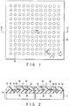
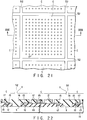
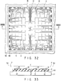
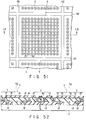
- FIG. 1 shows a semiconductor package according to a first embodiment of the present invention
- FIG. 2 is a sectional diagram taken along line II - II of FIG. 1.
- a semiconductor chip 10 has a square shape and measures 13.5 mm on a side.
- Semiconductor components having specific functions are formed on a semiconductor substrate 11.
- a plurality of pads (input and output terminals) 12 is formed on the substrate 11.
- the pads 12 are connected to the substrate 11, impurity regions within the substrate, and semiconductor components.
- these pads are mainly formed on peripheral portions of a semiconductor substrate.
- the pads 12 may be placed uniformly over the substrate by the use of a novel wafer process.
- a passivating film 13 is formed on the semiconductor substrate 11.
- This passivating film is the same as that for use with the conventional wafer processing and consists of an insulating material such as silicon oxide or silicon nitride.
- the passivating film 13 has openings 14 above the pads 12. The surface of the passivating film 13 is made flat.
- a plurality of interconnection lines 15 is formed on the passivating film 13, which constitutes one of features of the present invention.
- the interconnection lines 15 are connected to the pads 12 immediately below the openings 14 in the passivating film 13.
- Each interconnection line consists of a conductor such as aluminum or copper.
- a passivating film 16 is formed over the passivating film 13, which constitutes one of features of the present invention.
- This passivating film which has not been used with any conventional wafer process, covers the pads 12 completely. That is, the passivating film 16 will serve as a package.
- the passivating film 16 is set to have a thickness in the range from 0.05 to 0.2 mm so that it can fully serve as a package.
- the surface of the passivating film 16 is made flat so that electrodes may be formed thereon easily.
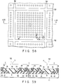
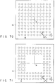
- the passivating film 16 has through holes 17 above the metal lines 15. When seen from above the semiconductor substrate 11, the through holes 17 are arranged in a grid form or array form. The through holes 17 are arranged symmetrically with respect to the central point ⁇ of the surface of the passivation insulating film 16.
- An electrically conductive layer 18 is formed within the through holes 17 in the passivating film 16 and on portions of the passivating film 16 adjacent to the through holes.
- the conductive layer 18 consists of copper, gold, nickel, or a two-layered structure of nickel and gold.
- the conductive layer 18 constitutes on the surface of the passivating film 16 contacts (electrodes) 19 for connection to external leads.
- a total of 144 metal contacts is formed in a 12 ⁇ 12 array at a pitch P of about 1mm with each contact having a circular shape of a diameter L of about 0.5 mm.
- the back and sides of the semiconductor substrate 11 are used as part of the package and the passivating film 16 formed over the font of the semiconductor substrate is used as part of the package.
- the semiconductor package can be formed in the wafer process, permitting the assembly process to be excluded as shown in FIG. 73.
- the semiconductor package of the present invention permits the cost of semiconductor products (finished products) to be lowered in comparison with conventional semiconductor packages requiring the assembly process.
- the semiconductor device test processing such as functional test, burn-in, etc., shown in FIG. 73 can be performed readily by connecting a socket to the contacts 19, providing test signals to semiconductor components and taking the test results from the semiconductor components.
- the size of the semiconductor products becomes equal to that of the semiconductor substrate 11. That is, the size of the semiconductor products can be decreased because the semiconductor package is integral with the semiconductor chip.
- the front of the semiconductor substrate 11 is completely coated with the passivating film 16, whereby the semiconductor package of the present invention is made resistant to humidity and external force.
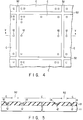
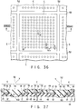
- an LSI structure (including semiconductor components) is formed within each of semiconductor chip regions C of a wafer 51 by means of the standard wafer processing.
- FIGS. 4 and 5 which are enlarged views of the portion A of FIG. 4, a plurality of pads 12 is formed on each semiconductor chip region C.
- these pads are formed mainly in peripheral portions of the semiconductor substrate 11.
- the pads may be formed evenly over the entire surface of the semiconductor substrate by means of a novel wafer process.
- Each semiconductor chip region C for example, has a square shape and measures about 13.5 mm on a side.
- a dicing line 52 is placed between semiconductor chip regions C.
- the passivating film 13 is formed on the semiconductor substrate 11 by means of CVD by way of example to thereby overlie semiconductor components.
- This passivating film 13 is the same as that used in the conventional wafer processing and consists of an insulating material such silicon oxide, silicon nitride or the like.
- the passivating film 13 After the surface of the passivating film 13 has been made flat by means of chemical mechanical polishing (CMP) by way of example, the passivating film is partly etched using a photoetching process (PEP). As a result, openings 14 are formed in the passivating film 13 each of which reaches the respective individual pads 12.
- CMP chemical mechanical polishing
- PEP photoetching process
- a conductive layer is formed over the entire surface of the passivating film 13.
- the conductive layer is patterned to create a plurality of interconnection lines 15 on the passivating film 13.
- Each interconnection line is connected to one of the pads 12 in the passivating film 13 that are located immediately below the openings 14.
- the interconnection line consists of an electrical conductor made of aluminum, copper, or the like.
- the passivating film 16 is formed over the passivating film 13 at a thickness in the range 0.05 to 0.2 mm by means of CVD by way of example.
- the surface of the passivating film 16 is flattened so that electrodes can be formed easily.
- the passivating film 16 is then etched partly by means of the PEP method to form through holes 17 in the passivating film 16 over the interconnection lines 15.
- the through holes 17 are arranged in the form of a grid or array.
- the holes 17 are arranged in a symmetrical relation with respect to the center of the surface of the insulating protection film 16.
- the conductive layer 18 is formed over the entire surface of the passivating film 16 by using the sputtering techniques.
- the conductive film 18 is then patterned to create, on the passivating film, the contacts (electrodes) 19 for connection to external leads.
- the contacts 19 are connected to the interconnection lines 15 immediately below the through-holes 17 in the passivating film 16.
- the contact 19 is made of copper, gold, nickel, or a two-layered structure of nickel and gold.
- the wafer is cut along its dicing lines denoted at 52 in FIG. 10 using a dicing apparatus, whereby a plurality of semiconductor chips 10 are obtained. At this point, semiconductor packages are also completed simultaneously.
- the semiconductor chip 10 may be subjected to heat treatment.
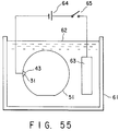
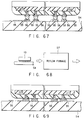
- solder balls 53 are formed on the respective contacts 19 for connection to external leads of the semiconductor package (corresponding to a fifth embodiment of the present invention). These solder balls are provided for easier mounting of the semiconductor package onto a printed-circuit board. Thus, the solder balls are not necessarily needed.
- the semiconductor package is placed on a printed-circuit board 54 so that the solder balls 53 may be brought into contact with predetermined portions of leads 55 on the printed-circuit board 54.
- the predetermined portions of the leads 55 of the printed-circuit board 54 are printed with solder 56.
- the semiconductor package (semiconductor chip) 10 and the printed-circuit board 54 are placed in a reflow furnace 57, then heated under predetermined conditions.
- FIG. 16 is a sectional diagram taken along line XVI - XVI of FIG. 15.
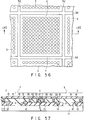
- a semiconductor chip 10 has a square shape and measures 13. 5 mm on a side.
- Semiconductor components with specific functions are formed within a semiconductor substrate 11.
- a plurality of pads (input and output terminals) are formed on the semiconductor substrate 11. Each pad is connected to the semiconductor substrate 11, an impurity region within the substrate, or a semiconductor component.
- these pads are formed mainly on peripheral portions of the semiconductor substrate 11.
- the pads 12 may be placed evenly over the entire surface of the semiconductor substrate 11 using a novel wafer process.
- a passivating film 13 is formed on the semiconductor substrate 11.
- This passivating film is the same as that used in the conventional wafer processing and consists of an insulating material such as silicon oxide, silicon nitride, or the like.
- the passivating film 13 has openings 14 over the pads 12.
- the surface of the passivating film is made flat.
- edges of the passivating film 13 do not reach the edges of the semiconductor substrate 11. That is, when viewed from above the substrate, the edges X of the passivating film 13 exist inside the edges Y of the semiconductor substrate.
- a plurality of interconnection lines 15 is formed on the passivating film 13, which constitutes one of features of the present invention. Each line 15 is connected to a respective one of the pads 12 immediately under the openings 14.
- the interconnection line is made of a conductor such as aluminum, copper or the like.
- a passivating film 16 is formed on the semiconductor substrate 11 and the passivating film 13, which constitutes one of the features of the present invention.
- the passivating film 16 is set to have a thickness sufficient to function as a package, i.e., a thickness in the range 0.05 to 0.2 mm.
- the surface of the passivating film 16 is made flat so that electrodes can be easily formed thereon.
- the passivating film 16 completely covers the edges of the passivating film 13. That is, the passivating film 13 is not exposed to outside. In comparison with the semiconductor package of FIGS. 1 and 2, therefore, the semiconductor package of the second embodiment is improved in moisture resistance because it is made difficult for moisture to penetrate into the interior of the semiconductor chip.
- the passivating film 16 has through holes 17 above the metal lines 15. When seen from above the semiconductor substrate 11, the through holes 17 are arranged in a grid form or array form. The through holes 17 are arranged symmetrically with respect to the central point ⁇ of the surface of the passivation insulating film 16.
- An electrically conductive layer 18 is formed within the through holes 17 in the passivating film 16 and on portions of the passivating film 16 adjacent to the through holes.
- the conductive layer 18 is made of copper, gold, nickel, or a two-layered structure of nickel and gold.
- the conductive layer 18 constitutes on the surface of the passivating film 16 contacts (electrodes) 19 for connection to external leads.
- a total of 144 metal contacts is formed in a 12 ⁇ 12 array at a pitch P of about 1mm with each contact having a circular shape of a diameter L of about 0.5 mm.
- the back and sides of the semiconductor substrate 11 are used as part of the package and the passivating film 16 formed over the upper surface of the semiconductor substrate is used as part of the package.
- the semiconductor package can be formed in the wafer processing, permitting the assembly process to be excluded as shown in FIG. 73.
- the semiconductor package of the present invention permits the cost of semiconductor products (finished products) to be lowered in comparison with the conventional semiconductor packages requiring the assembly process.
- the semiconductor device test processing such as functional test, burn-in, etc., shown in FIG. 73 can be performed readily by connecting a socket to the metal contacts 19, providing test signals to semiconductor components and taking the test results from the semiconductor components.
- the semiconductor products are made equal to the size of the semiconductor substrate 11. That is, the size of the semiconductor products can be decreased because the semiconductor package is integral with the semiconductor chip.
- the passivating film 16 covers completely the edges X of the passivating film 13 and contacts the edges Y of the semiconductor substrate 11. Thus, only the interface between the semiconductor substrate 11 and the passivating film 16 is exposed to outside, allowing the semiconductor package to be very resistant to humidity and external force.
- an LSI structure (including semiconductor components) is formed within each of semiconductor chip regions C of a wafer 51 by means of the standard wafer processing.
- FIG. 17 which is an enlarged view of A of FIG. 3 and FIG. 18 which is a sectional view taken along line XVIII - XVIII of FIG. 17, a plurality of pads 12 is formed on each semiconductor chip region C.
- these pads are formed mainly in peripheral portions of the semiconductor substrate 11.
- the pads may be formed evenly over the entire surface of the semiconductor substrate by means of a novel wafer process.
- Each semiconductor chip region C for example, has a square shape and measures about 13.5 mm on a side.
- a dicing line 52 is placed between semiconductor chip regions C.
- the passivating film 13 is formed on the semiconductor substrate 11 by means of CVD by way of example to thereby cover semiconductor components.
- This passivating film 13 is the same as that used in the conventional wafer process and consists of an insulating material such silicon oxide, silicon nitride or the like.
- the passivating film 13 After the surface of the passivating film 13 has been made flat by means of CMP by way of example, the passivating film is partly etched using PEP. As a result, openings 14 are formed in the passivating film 13 each of which reaches the respective individual pads 12.
- the passivating film 13 is partly etched away to remove the passivating film 13 in areas including the area immediately under the dicing lines 52.
- the edges X of the passivating film 13 are placed inside the semiconductor chip region C (its edges Y finally become the edges of the semiconductor substrate 11).
- a conductive layer is formed over the entire surface of the passivating film 13.
- the conductive layer is patterned to create a plurality of interconnection lines 15 on the passivating film 13.
- Each interconnection line is connected to one of the pads 12 in the passivating film 13 that are located immediately below the openings 14.
- the interconnection line consists of an electrical conductor made of aluminum, copper, or the like.
- the passivating film 16 is formed over the passivating film 13 at a thickness in the range 0.05 to 0.2 mm by means of CVD by way of example.
- the surface of the passivating film 16 is flattened so that electrodes can be easily formed thereon.
- the passivating film 16 is then etched partly by means of the PEP method to form through holes 17 in the passivating film 16 over the interconnection lines 15.
- the through holes 17 are arranged in the form of a grid or array.
- the holes 17 are arranged in a symmetrical relation with respect to the center ⁇ of the surface of the insulating protection film 16.
- the conductive layer 18 is formed over the entire surface of the passivating film 16 by using the sputtering method.
- the conductive film 18 is then patterned to create, on the passivating film, the contacts (electrodes) 19 for connection to external leads.
- the contacts 19 are connected to the interconnection lines 15 immediately below the through holes 17 in the passivating film 16.
- the contact 19 is made of copper, gold, nickel, or a two-layered structure of nickel and gold.
- the wafer is cut along its dicing lines denoted at 52 in FIG. 23 using a dicing apparatus, whereby a plurality of semiconductor chips 10 are obtained. At this point, semiconductor packages are also completed simultaneously.
- the semiconductor chip 10 may be subjected to heat treatment.
- solder balls 53 are formed on the contacts 19 for connection to external leads of the semiconductor package (corresponding to a sixth embodiment of the present invention). These solder balls are provided for easier mounting of the semiconductor package onto a printed-circuit board. Thus, the solder balls are not necessarily needed.
- the semiconductor package is placed on a printed-circuit board 54 so that the solder balls 53 may be brought into contact with predetermined portions of leads 55 on the printed-circuit board 54.
- the predetermined portions of the leads 55 of the printed-circuit board 54 are printed with solder 56.
- the semiconductor package (semiconductor chip) 10 and the printed-circuit board 54 are placed in a reflow furnace 57, then heated under predetermined conditions.
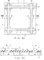
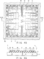
- FIG. 29 is a sectional diagram taken along line XXIX - XXIX of FIG. 28.
- a semiconductor chip 10 has a square shape and measures 13.5 mm on a side.
- Semiconductor components with specific functions are formed within a semiconductor substrate 11.
- a plurality of pads (input and output terminals) are formed on the semiconductor substrate 11. Each pad is connected to the semiconductor substrate 11, an impurity region within the substrate, or a semiconductor component.
- these pads are formed mainly on peripheral portions of the semiconductor substrate 11.
- the pads 12 may be placed evenly over the entire surface of the semiconductor substrate 11 using a novel wafer process.
- a passivating film 13 is formed on the semiconductor substrate 11.
- This passivating film is the same as that used in conventional wafer processing and consists of an insulating material such as silicon oxide, silicon nitride, or the like.
- the passivating film 13 has openings 14 over the pads 12.
- the surface of the passivating film is made flat.
- edges of the passivating film 13 do not reach the edges of the semiconductor substrate 11. That is, when viewed from above the substrate, the edges X of the passivating film 13 exist inside the edges Y of the semiconductor substrate. Between the edges X of the passivating film 13 and the edges Y of the semiconductor substrate 11 is formed a groove 60 along the edges of the semiconductor substrate.
- a plurality of interconnection lines 15 is formed on the passivating film 13, which constitutes one of features of the present invention. Each line 15 is connected to a respective one of the pads 12 immediately under the openings 14.
- the interconnection line is made of a conductor such as aluminum, copper or the like.
- a passivating film 16 is formed on the semiconductor substrate 11 and the passivating film 13, which constitutes one of the features of the present invention.
- the passivating film 16 is set to have a thickness sufficient to function as a package, i.e., a thickness in the range 0.05 to 0.2 mm.
- the surface of the passivating film 16 is made flat so that electrodes can be easily formed thereon.
- the passivating film 16 completely covers the edges X of the passivating film 13. That is, the passivating film 13 is not exposed to outside. In comparison with the semiconductor package of FIGS. 1 and 2, therefore, the semiconductor package of the third embodiment is improved in moisture resistance because it is made difficult for moisture to penetrate into the interior of the semiconductor chip.
- the passivating film 16 has through holes 17 above the metal lines 15. When seen from above the semiconductor substrate 11, the through holes 17 are arranged in a grid form or array form. The through holes 17 are arranged symmetrically with respect to the central point ⁇ of the surface of the passivation insulating film 16.
- An electrically conductive layer 18 is formed within the through holes 17 in the passivating film 16 and on portions of the passivating film 16 adjacent to the through holes.
- the conductive layer 18 is made of copper, gold, nickel, or a two-layered structure of nickel and gold.
- the conductive layer 18 constitutes on the surface of the passivating film 16 metal contacts (electrodes) 19 for connection to external leads.
- a total of 144 metal contacts is formed in a 12 ⁇ 12 array at a pitch P of about 1 mm with each metal contact having a circular shape of a diameter L of about 0.5 mm.
- the back and sides of the semiconductor substrate 11 are used as part of the package and the passivating film 16 formed over the front of the semiconductor substrate is used as part of the package.
- the semiconductor package can be formed in the wafer process, permitting the assembly process to be excluded as shown in FIG. 73.
- the semiconductor package of the present invention permits the cost of semiconductor products (finished products) to be lowered in comparison with the conventional semiconductor package requiring the assembly process.
- the semiconductor device test process such as functional test, burn-in, etc., shown in FIG. 73 can be performed readily by connecting a socket to the metal contacts 19, providing test signals to semiconductor components and taking the test results from the semiconductor components.
- the semiconductor products are made equal to the size of the semiconductor substrate 11. That is, the size of the semiconductor products can be decreased because the semiconductor package is integral with the semiconductor chip.
- the passivating film 16 covers completely the edges X of the passivating film 13 and contacts the edges Y of the semiconductor substrate 11. Thus, only the interface between the semiconductor substrate 11 and the passivating film 16 is exposed to outside, allowing the semiconductor package to be very resistant to humidity and external force.
- an LSI structure (including semiconductor components) is formed within each of semiconductor chip regions C of a wafer 51 by means of the standard wafer process.
- FIG. 30 which is an enlarged view of A of FIG. 3 and FIG. 31 which is a sectional view taken along line XXXI - XXXI of FIG. 30, a plurality of pads 12 is formed on each semiconductor chip region C.
- these pads are formed mainly in peripheral portions of the semiconductor substrate 11.
- the pads may be formed evenly over the entire surface of the semiconductor substrate by means of a novel wafer process.
- Each semiconductor chip region C for example, has a square shape and measures about 13.5 mm on a side.
- a dicing line 52 is placed between semiconductor chip regions C.
- the passivating film 13 is formed on the semiconductor substrate 11 by means of CVD by way of example to thereby cover semiconductor components.
- This passivating film 13 is the same as that used in the conventional wafer process and consists of an insulating material such silicon oxide, silicon nitride or the like.
- the passivating film 13 After the surface of the passivating film 13 has been made flat by means of CMP by way of example, the passivating film is partly etched using PEP. As a result, openings 14 are formed in the passivating film 13 each of which reaches the respective individual pads 12.
- the passivating film 13 is partly etched away to remove the passivating film 13 and the semiconductor substrate in areas including the area immediately under the dicing lines 52.
- the edges X of the passivating film 13 are placed inside the semiconductor chip region C (its edges Y finally become the edges of the semiconductor substrate 11).
- the groove 60 is formed which extends along the dicing lines 52 and has a width greater than the width of the dicing lines. The groove is formed by overetching the semiconductor substrate 11 for the purpose of completely removing the passivating film 13 immediately under the dicing lines 52.
- a conductive layer is formed over the entire surface of the passivating film 13.
- the conductive layer is patterned to create a plurality of interconnection lines 15 on the passivating film 13.
- Each interconnection line is connected to one of the pads 12 in the passivating film 13 that are located immediately below the openings 14.
- the interconnection line consists of an electrical conductor made of aluminum, copper, or the like.
- the passivating film 16 is foamed over the passivating film 13 at a thickness in the range 0.05 to 0.2 mm by means of CVD by way of example.
- the surface of the passivating film 16 is flattened so that electrodes can be easily formed thereon.
- the passivating film 16 is then etched partly by means of the PEP method to form through holes 17 in the passivating film 16 over the interconnection lines 15.
- the through holes 17 are arranged in the form of a grid or array.
- the holes 17 are arranged in a symmetrical relation with respect to the center ⁇ of the surface of the insulating protection film 16.
- the conductive layer 18 is formed over the entire surface of the passivating film 16 by using the sputtering method.
- the conductive film 18 is then patterned to create, on the passivating film, the contacts (electrodes) 19 for connection to external leads.
- the contacts 19 are connected to the interconnection lines 15 immediately below the through holes 17 in the passivating film 16.
- the contact 19 is made of copper, gold, nickel, or a two-layered structure of nickel and gold.
- the wafer is cut along its dicing lines denoted at 52 in FIG. 36 using a dicing apparatus, whereby a plurality of semiconductor chips 10 are obtained. At this point, semiconductor packages are also completed simultaneously.
- the semiconductor chip 10 may be subjected to heat treatment.
- solder balls 53 are formed on the contacts 19 for connection to external leads of the semiconductor package (corresponding to a seventh embodiment of the present invention). These solder balls are provided for easier mounting of the semiconductor package onto a printed-circuit board. Thus, the solder balls are not necessarily needed.
- the semiconductor package is placed on a printed-circuit board 54 so that the solder balls 53 may be brought into contact with predetermined portions of leads 55 on the printed-circuit board 54.
- the predetermined portions of the leads 55 of the printed-circuit board 54 are printed with solder 56.
- the semiconductor package (semiconductor chip) 10 and the printed-circuit board 54 are placed in a reflow furnace 57, then heated under predetermined conditions.
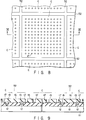
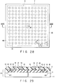
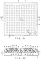
- FIG. 41 there is shown a semiconductor package according to a fourth embodiment of the present invention.
- FIG. 42 is a sectional diagram taken along line XLII - XLII of FIG. 41.
- a semiconductor chip 10 has a square shape and measures 13.5 mm on a side.
- Semiconductor components with specific functions are formed within a semiconductor substrate 11.
- a plurality of pads (input and output terminals) is formed on the semiconductor substrate 11. Each pad is connected to the semiconductor substrate 11, an impurity region within the substrate, or a semiconductor component.
- these pads are formed mainly on peripheral portions of the semiconductor substrate 11.
- the pads 12 may be placed evenly over the entire surface of the semiconductor substrate 11 using a novel wafer process.
- a passivating film 13 is formed on the semiconductor substrate 11.
- This passivating film is the same as that used in the conventional wafer process and consists of an insulating material such as silicon oxide, silicon nitride, or the like.
- the passivating film 13 has openings 14 over the pads 12.
- the surface of the passivating film is made flat.
- edges of the passivating film 13 do not reach the edges of the semiconductor substrate 11. That is, when viewed from above the substrate, the edges X of the passivating film 13 exist inside the edges Y of the semiconductor substrate. Between the edges X of the passivating film 13 and the edges Y of the semiconductor substrate 11 is formed a groove 60 along the edges of the semiconductor substrate 11.
- a plurality of interconnection lines 15 is formed on the passivating film 13, which constitutes one of features of the present invention. Each line 15 is connected to a respective one of the pads 12 immediately under the openings 14.
- the interconnection line is made of a conductor such as aluminum, copper or the like.
- a passivating film 16 is formed on the semiconductor substrate 11 and the passivating film 13, which constitutes one of the features of the present invention.
- the passivating film 16 is set to have a thickness sufficient to function as a package, i.e., a thickness in the range 0.05 to 0.2 mm.
- the surface of the passivating film 16 is made flat so that electrodes can be easily formed thereon.
- the passivating film 16 completely covers the edges X of the passivating film 13. That is, the passivating film 13 is not exposed to outside. In comparison with the semiconductor package of FIGS. 1 and 2, therefore, the semiconductor package of the fourth embodiment is improved in moisture resistance because it is made difficult for moisture to penetrate into the interior of the semiconductor chip.
- the passivating film 16 has through holes 17 above the metal lines 15. When seen from above the semiconductor substrate 11, the through holes 17 are arranged in a grid form or array form. The through holes 17 are arranged symmetrically with respect to the central point ⁇ of the surface of the passivation insulating film 16.
- a thin layer 31 of metal is formed within the through holes 17 and on those portions of the passivating film 16 which are adjacent to the through holes.
- the thickness of the metal layer 31 is set sufficiently small in comparison with the size (diameter) of the through holes 17.
- the metal layer 31 is made of, for example, titan (about 0.05 ⁇ m in thickness), nickel (about 0.3 ⁇ m in thickness), palladium (about 0.1 ⁇ m in thickness), or a stacked layer of these materials.
- a plated layer 32 is formed on the metal layer 31 within the through holes and on the metal layer 31 adjacent to the through holes.
- the plated layer is made of copper, gold, nickel or a two-layered structure of nickel and gold.
- the plated layer constitutes contacts (electrodes) 18 for connection to external leads on the surface of the passivating film 16.
- the metal layer 31 functions as a plating electrode in forming the plated layer 32 by means of electroplating.
- the metal layer also functions as barrier metal for preventing diffusion of metallic atoms and alloy reaction.
- a total of 144 metal contacts is formed in a 12 ⁇ 12 array at a pitch P of about 1mm with each metal contact having a circular shape of a diameter L of about 0.5 mm.
- the height of the metal contacts 19 is set to range from some micrometers to 10 micrometers.
- the back and sides of the semiconductor substrate 11 are used as part of the package and the passivating film 16 formed over the upper surface of the semiconductor substrate is used as part of the package.
- the semiconductor package can be formed in the wafer process, permitting the assembly process to be excluded as shown in FIG. 73.
- the semiconductor package of the present invention permits the cost of semiconductor products (finished products) to be lowered in comparison with the conventional semiconductor package requiring the assembly process.
- the semiconductor device test process such as functional test, burn-in, etc., shown in FIG. 73 can be performed readily by connecting a socket to the metal contacts 19, providing test signals to semiconductor components and taking the test results from the semiconductor components.
- the semiconductor products is made equal to the size of the semiconductor substrate 11. That is, the size of the semiconductor products can be decreased because the semiconductor package is integral with the semiconductor chip.
- the passivating film 16 covers completely the edges X of the passivating film 13 and contacts the edges Y of the semiconductor substrate 11. Thus, only the interface between the semiconductor substrate 11 and the passivating film 16 is exposed to outside, allowing the semiconductor package to be very resistant to humidity and external force.
- the metal layer 31 serving as the plating electrode is placed immediately under the plated layer 32, the metal contacts 19 can be formed at low cost and easily by means of electroplating.
- an LSI structure (including semiconductor components) is formed within each of semiconductor chip regions C of a wafer 51 by means of the standard wafer processing.
- FIG. 43 which is an enlarged view of A of FIG. 3 and FIG. 44 which is a sectional view taken along line XLIV - XLIV of FIG. 43
- a plurality of pads 12 is formed on each semiconductor chip region C.
- these pads are formed mainly in peripheral portions of the semiconductor substrate 11.
- the pads may be formed evenly over the entire surface of the semiconductor substrate by means of a novel wafer process.
- Each semiconductor chip region C for example, has a square shape and measures about 13.5 mm on a side.
- a dicing line 52 is placed between semiconductor chip regions C.
- the passivating film 13 is formed on the semiconductor substrate 11 by means of CVD by way of example to thereby cover semiconductor components.
- This passivating film 13 is the same as that used in the conventional wafer process and consists of an insulating material such silicon oxide, silicon nitride or the like.
- the passivating film 13 After the surface of the passivating film 13 has been made flat by means of CMP by way of example, the passivating film is partly etched using PEP. As a result, openings 14 are formed in the passivating film 13 each of which reaches the respective individual pads 12.
- the passivating film 13 is partly etched away to remove the passivating film 13 in areas including the area immediately under the dicing lines 52.
- the edges X of the passivating film 13 are placed inside the semiconductor chip region C (its edges Y finally become the edges of the semiconductor substrate 11).
- a conductive layer is formed over the entire surface of the passivating film 13.
- the conductive layer is patterned to create a plurality of interconnection lines 15 on the passivating film 13.
- Each interconnection line is connected to one of the pads 12 in the passivating film 13 that are located immediately below the openings 14.
- the interconnection line consists of an electrical conductor made of aluminum, copper, or the like.
- the passivating film 16 is formed over the passivating film 13 at a thickness in the range 0.05 to 0.2 mm by means of CVD by way of example.
- the surface of the passivating film 16 is flattened so that electrodes can be easily formed thereon.
- the passivating film 16 is then etched partly by means of the PEP method to form through holes 17 in the passivating film 16 over the interconnection lines 15.
- the through holes 17 are arranged in the form of a grid or array.
- the holes 17 are arranged in a symmetrical relation with respect to the center ⁇ of the surface of the insulating protection film 16.
- the metal layer 31 is formed at the bottom and on the sides of the through holes 17 and over the entire surface of the passivating film 16 (the entire surface of the wafer) by using the sputtering method.
- the metal layer is formed by depositing, for example, a layer of titan of about 0.05 micrometer thickness, a layer of nickel of about 0.3 micrometer thickness and a layer of palladium of about 0.1 micrometer thickness in sequence.
- a resist layer 41 is formed over the entire surface of the metal layer 31, then patterned to form openings 42, which are greater in diameter than the through holes 17, in those portions of the resist layer which are located over the through holes.
- the openings 52 are made equal in size to the package contacts for connection to external leads.
- one or more voltage supplying openings 43 are formed at the edge of the wafer 51.
- a single opening is formed.
- the opening 43 may be formed in a predetermined inside portion of the wafer 51 instead of being formed in its edge portion.
- a plating bath 61 is prepared which is filled with a predetermined solution.
- One end of a power supply 64 is connected to the metal layer 31 of the wafer 51 which is exposed through the opening 43 with the other end being connected to a plating electrode 63. After that, the wafer 51 and the plating electrode 63 are immersed in the solution 62 in the plating bath 61.
- the plated layer 32 can be made of various materials by changing the solution 62 and the electrode 63.
- the plated layer 32 is made of copper, gold, nickel, or a two-layered structure of nickel and gold.
- the package contacts 19 are formed on the surface of the passivating film 16 as shown in FIGS. 58 and 59.
- the wafer is cut along its dicing lines denoted at 52 in FIG. 58 using a dicing apparatus, whereby a plurality of semiconductor chips 10 are obtained. At this point, semiconductor packages are also completed simultaneously.
- the semiconductor chip 10 may be subjected to heat treatment.
- solder balls 53 are formed on the contacts 19 for connection to external leads of the semiconductor package (corresponding to an eighth embodiment of the present invention). These solder balls are provided for easier mounting of the semiconductor package onto a printed-circuit board. Thus, the solder balls are not necessarily needed.
- the semiconductor package is placed on a printed-circuit board 54 so that the solder balls 53 may be brought into contact with predetermined portions of leads 55 on the printed-circuit board 54.
- the predetermined portions of the leads 55 of the printed-circuit board 54 are printed with solder 56.
- the semiconductor package 10 and the printed-circuit board 54 are placed in a reflow furnace 57, then heated under predetermined conditions.
- FIG. 70 shows a semiconductor package according to a ninth embodiment of the present invention.
- the feature of this package is its way of arranging the contacts 19 for connection to external leads.
- a total of 121 contacts are formed in a grid form (11 ⁇ 11 array) at a pitch P of about 1 mm.
- one of the contacts 19 is located at the central point ⁇ of the semiconductor package.
- the contacts 19 will be arranged symmetrically with respect to the central point ⁇ of the semiconductor package.
- FIG. 71 shows a semiconductor package according to a tenth embodiment of the present invention, which features the way the contacts 19 are arranged.
- a total of 121 contacts are formed on the periphery of the semiconductor package at a pitch P of about 1 mm.
- this semiconductor package can be considered to have the 6 ⁇ 6 array of contacts to be located in the center of the semiconductor package of FIG. 1 omitted.
- the contacts 19 are placed symmetrically with respect to the center ⁇ of the semiconductor package.
- FIG. 72 shows a semiconductor package according to an eleventh embodiment of the present invention, which features the way the contacts 19 are arranged.
- a total of 96 contacts are formed on the periphery of the semiconductor package at a pitch P of about 1 mm.
- this semiconductor package can be considered to have the 5 ⁇ 5 array of contacts to be located in the center of the semiconductor package of FIG. 1 omitted.
- the contacts 19 are placed symmetrically with respect to the center ⁇ of the semiconductor package.
Applications Claiming Priority (6)
| Application Number | Priority Date | Filing Date | Title |
|---|---|---|---|
| JP23904294 | 1994-10-03 | ||
| JP239042/94 | 1994-10-03 | ||
| JP23904294 | 1994-10-03 | ||
| JP221827/95 | 1995-08-30 | ||
| JP22182795 | 1995-08-30 | ||
| JP22182795 | 1995-08-30 |
Publications (3)
| Publication Number | Publication Date |
|---|---|
| EP0706208A2 true EP0706208A2 (de) | 1996-04-10 |
| EP0706208A3 EP0706208A3 (de) | 1998-01-14 |
| EP0706208B1 EP0706208B1 (de) | 2002-06-12 |
Family
ID=26524531
Family Applications (1)
| Application Number | Title | Priority Date | Filing Date |
|---|---|---|---|
| EP95115550A Expired - Lifetime EP0706208B1 (de) | 1994-10-03 | 1995-10-02 | Verfahren zur Herstellung einer Halbleiterpackung integral mit Halbleiterchip |
Country Status (4)
| Country | Link |
|---|---|
| US (1) | US5892273A (de) |
| EP (1) | EP0706208B1 (de) |
| KR (1) | KR960015869A (de) |
| DE (1) | DE69527017T2 (de) |
Cited By (6)
| Publication number | Priority date | Publication date | Assignee | Title |
|---|---|---|---|---|
| EP0923128A1 (de) * | 1997-06-23 | 1999-06-16 | Citizen Watch Co., Ltd. | Halbleiterpackung und herstellungsverfahren dafür |
| WO2000055910A1 (en) * | 1999-03-15 | 2000-09-21 | Hitachi, Ltd. | Semiconductor device and semiconductor module |
| WO2001035461A1 (en) * | 1999-11-11 | 2001-05-17 | Casio Computer Co., Ltd. | Semiconductor device and method of manufacturing the same |
| WO2002052646A1 (en) * | 2000-12-22 | 2002-07-04 | Koninklijke Philips Electronics N.V. | Integrated circuit device |
| WO2003049184A1 (en) * | 2001-12-07 | 2003-06-12 | Fujitsu Limited | Semiconductor device and method for manufacturing the same |
| US6603191B2 (en) | 2000-05-18 | 2003-08-05 | Casio Computer Co., Ltd. | Semiconductor device and method of manufacturing the same |
Families Citing this family (55)
| Publication number | Priority date | Publication date | Assignee | Title |
|---|---|---|---|---|
| AU4321997A (en) | 1996-10-17 | 1998-05-15 | Seiko Epson Corporation | Semiconductor device, method of its manufacture, circuit substrate, and film carrier tape |
| US6194313B1 (en) * | 1997-04-30 | 2001-02-27 | Texas Instruments Incorporated | Method for reducing recess for the formation of local interconnect and or plug trench fill for etchback process |
| JP3173439B2 (ja) * | 1997-10-14 | 2001-06-04 | 松下電器産業株式会社 | セラミック多層基板及びその製造方法 |
| JP3497722B2 (ja) * | 1998-02-27 | 2004-02-16 | 富士通株式会社 | 半導体装置及びその製造方法及びその搬送トレイ |
| US6642136B1 (en) | 2001-09-17 | 2003-11-04 | Megic Corporation | Method of making a low fabrication cost, high performance, high reliability chip scale package |
| JP4239310B2 (ja) * | 1998-09-01 | 2009-03-18 | ソニー株式会社 | 半導体装置の製造方法 |
| US8021976B2 (en) | 2002-10-15 | 2011-09-20 | Megica Corporation | Method of wire bonding over active area of a semiconductor circuit |
| US6495442B1 (en) * | 2000-10-18 | 2002-12-17 | Magic Corporation | Post passivation interconnection schemes on top of the IC chips |
| US7405149B1 (en) | 1998-12-21 | 2008-07-29 | Megica Corporation | Post passivation method for semiconductor chip or wafer |
| US6936531B2 (en) * | 1998-12-21 | 2005-08-30 | Megic Corporation | Process of fabricating a chip structure |
| US7381642B2 (en) * | 2004-09-23 | 2008-06-03 | Megica Corporation | Top layers of metal for integrated circuits |
| US6965165B2 (en) * | 1998-12-21 | 2005-11-15 | Mou-Shiung Lin | Top layers of metal for high performance IC's |
| JP3577421B2 (ja) * | 1999-01-25 | 2004-10-13 | 新光電気工業株式会社 | 半導体装置用パッケージ |
| US6326701B1 (en) * | 1999-02-24 | 2001-12-04 | Sanyo Electric Co., Ltd. | Chip size package and manufacturing method thereof |
| WO2000065647A1 (en) | 1999-04-22 | 2000-11-02 | International Rectifier Corporation | Chip scale package |
| US6373268B1 (en) | 1999-05-10 | 2002-04-16 | Intel Corporation | Test handling method and equipment for conjoined integrated circuit dice |
| US6181569B1 (en) * | 1999-06-07 | 2001-01-30 | Kishore K. Chakravorty | Low cost chip size package and method of fabricating the same |
| US6322903B1 (en) | 1999-12-06 | 2001-11-27 | Tru-Si Technologies, Inc. | Package of integrated circuits and vertical integration |
| US6653740B2 (en) | 2000-02-10 | 2003-11-25 | International Rectifier Corporation | Vertical conduction flip-chip device with bump contacts on single surface |
| US7271489B2 (en) * | 2003-10-15 | 2007-09-18 | Megica Corporation | Post passivation interconnection schemes on top of the IC chips |
| US6815324B2 (en) * | 2001-02-15 | 2004-11-09 | Megic Corporation | Reliable metal bumps on top of I/O pads after removal of test probe marks |
| US6818545B2 (en) * | 2001-03-05 | 2004-11-16 | Megic Corporation | Low fabrication cost, fine pitch and high reliability solder bump |
| TWI313507B (en) * | 2002-10-25 | 2009-08-11 | Megica Corporatio | Method for assembling chips |
| US7902679B2 (en) * | 2001-03-05 | 2011-03-08 | Megica Corporation | Structure and manufacturing method of a chip scale package with low fabrication cost, fine pitch and high reliability solder bump |
| US7099293B2 (en) * | 2002-05-01 | 2006-08-29 | Stmicroelectronics, Inc. | Buffer-less de-skewing for symbol combination in a CDMA demodulator |
| US7932603B2 (en) | 2001-12-13 | 2011-04-26 | Megica Corporation | Chip structure and process for forming the same |
| JP2003188313A (ja) * | 2001-12-20 | 2003-07-04 | Matsushita Electric Ind Co Ltd | 半導体装置およびその製造方法 |
| US6673698B1 (en) | 2002-01-19 | 2004-01-06 | Megic Corporation | Thin film semiconductor package utilizing a glass substrate with composite polymer/metal interconnect layers |
| TW584950B (en) * | 2001-12-31 | 2004-04-21 | Megic Corp | Chip packaging structure and process thereof |
| TW503496B (en) * | 2001-12-31 | 2002-09-21 | Megic Corp | Chip packaging structure and manufacturing process of the same |
| TW544882B (en) * | 2001-12-31 | 2003-08-01 | Megic Corp | Chip package structure and process thereof |
| TWI245402B (en) * | 2002-01-07 | 2005-12-11 | Megic Corp | Rod soldering structure and manufacturing process thereof |
| US20030218246A1 (en) * | 2002-05-22 | 2003-11-27 | Hirofumi Abe | Semiconductor device passing large electric current |
| US6713317B2 (en) | 2002-08-12 | 2004-03-30 | Semiconductor Components Industries, L.L.C. | Semiconductor device and laminated leadframe package |
| US20040036171A1 (en) * | 2002-08-22 | 2004-02-26 | Farnworth Warren M. | Method and apparatus for enabling a stitch wire bond in the absence of discrete bump formation, semiconductor device assemblies and electronic systems including same |
| US7115998B2 (en) | 2002-08-29 | 2006-10-03 | Micron Technology, Inc. | Multi-component integrated circuit contacts |
| US6768186B2 (en) | 2002-10-15 | 2004-07-27 | Semiconductor Components Industries, L.L.C. | Semiconductor device and laminated leadframe package |
| WO2005024912A2 (en) * | 2003-09-09 | 2005-03-17 | Intel Corporation | Methods of processing thick ild layers using spray coating or lamination for c4 wafer level thick metal integrated flow |
| US6977435B2 (en) * | 2003-09-09 | 2005-12-20 | Intel Corporation | Thick metal layer integrated process flow to improve power delivery and mechanical buffering |
| US7459790B2 (en) * | 2003-10-15 | 2008-12-02 | Megica Corporation | Post passivation interconnection schemes on top of the IC chips |
| US7394161B2 (en) * | 2003-12-08 | 2008-07-01 | Megica Corporation | Chip structure with pads having bumps or wirebonded wires formed thereover or used to be tested thereto |
| US8022544B2 (en) | 2004-07-09 | 2011-09-20 | Megica Corporation | Chip structure |
| US7465654B2 (en) * | 2004-07-09 | 2008-12-16 | Megica Corporation | Structure of gold bumps and gold conductors on one IC die and methods of manufacturing the structures |
| US8067837B2 (en) | 2004-09-20 | 2011-11-29 | Megica Corporation | Metallization structure over passivation layer for IC chip |
| US7521805B2 (en) * | 2004-10-12 | 2009-04-21 | Megica Corp. | Post passivation interconnection schemes on top of the IC chips |
| US8294279B2 (en) * | 2005-01-25 | 2012-10-23 | Megica Corporation | Chip package with dam bar restricting flow of underfill |
| US7473999B2 (en) * | 2005-09-23 | 2009-01-06 | Megica Corporation | Semiconductor chip and process for forming the same |
| TW200717743A (en) * | 2005-10-03 | 2007-05-01 | Rohm Co Ltd | Semiconductor device |
| DE102006003931B3 (de) * | 2006-01-26 | 2007-08-02 | Infineon Technologies Ag | Halbleiterbauteil mit oberflächenmontierbaren Außenkontakten und Verfahren zur Herstellung desselben |
| US8836146B2 (en) * | 2006-03-02 | 2014-09-16 | Qualcomm Incorporated | Chip package and method for fabricating the same |
| US7768075B2 (en) * | 2006-04-06 | 2010-08-03 | Fairchild Semiconductor Corporation | Semiconductor die packages using thin dies and metal substrates |
| US8022552B2 (en) | 2006-06-27 | 2011-09-20 | Megica Corporation | Integrated circuit and method for fabricating the same |
| TWI370515B (en) * | 2006-09-29 | 2012-08-11 | Megica Corp | Circuit component |
| US8193636B2 (en) * | 2007-03-13 | 2012-06-05 | Megica Corporation | Chip assembly with interconnection by metal bump |
| US8030775B2 (en) | 2007-08-27 | 2011-10-04 | Megica Corporation | Wirebond over post passivation thick metal |
Family Cites Families (9)
| Publication number | Priority date | Publication date | Assignee | Title |
|---|---|---|---|---|
| US4107726A (en) * | 1977-01-03 | 1978-08-15 | Raytheon Company | Multilayer interconnected structure for semiconductor integrated circuit |
| JPS6461934A (en) * | 1987-09-02 | 1989-03-08 | Nippon Denso Co | Semiconductor device and manufacture thereof |
| US5220199A (en) * | 1988-09-13 | 1993-06-15 | Hitachi, Ltd. | Semiconductor integrated circuit device in which a semiconductor chip is mounted with solder bumps for mounting to a wiring substrate |
| US5250468A (en) * | 1990-02-05 | 1993-10-05 | Mitsubishi Denki Kabushiki Kaisha | Method of manufacturing semiconductor device including interlaying insulating film |
| JPH05160292A (ja) * | 1991-06-06 | 1993-06-25 | Toshiba Corp | 多層パッケージ |
| US5360988A (en) * | 1991-06-27 | 1994-11-01 | Hitachi, Ltd. | Semiconductor integrated circuit device and methods for production thereof |
| JPH0574776A (ja) * | 1991-09-13 | 1993-03-26 | Hitachi Ltd | 半導体装置の実装構造 |
| JP2796919B2 (ja) * | 1992-05-11 | 1998-09-10 | インターナショナル・ビジネス・マシーンズ・コーポレーション | メタライゼーション複合体および半導体デバイス |
| US5581122A (en) * | 1994-10-25 | 1996-12-03 | Industrial Technology Research Institute | Packaging assembly with consolidated common voltage connections for integrated circuits |
-
1995
- 1995-10-02 US US08/537,396 patent/US5892273A/en not_active Expired - Lifetime
- 1995-10-02 KR KR1019950033642A patent/KR960015869A/ko not_active Application Discontinuation
- 1995-10-02 DE DE69527017T patent/DE69527017T2/de not_active Expired - Lifetime
- 1995-10-02 EP EP95115550A patent/EP0706208B1/de not_active Expired - Lifetime
Non-Patent Citations (1)
| Title |
|---|
| None |
Cited By (11)
| Publication number | Priority date | Publication date | Assignee | Title |
|---|---|---|---|---|
| EP0923128A1 (de) * | 1997-06-23 | 1999-06-16 | Citizen Watch Co., Ltd. | Halbleiterpackung und herstellungsverfahren dafür |
| EP0923128A4 (de) * | 1997-06-23 | 2004-07-21 | Citizen Watch Co Ltd | Halbleiterpackung und herstellungsverfahren dafür |
| WO2000055910A1 (en) * | 1999-03-15 | 2000-09-21 | Hitachi, Ltd. | Semiconductor device and semiconductor module |
| US6927489B1 (en) | 1999-03-15 | 2005-08-09 | Renesas Technology Corp. | Semiconductor device provided with rewiring layer |
| WO2001035461A1 (en) * | 1999-11-11 | 2001-05-17 | Casio Computer Co., Ltd. | Semiconductor device and method of manufacturing the same |
| US6607970B1 (en) | 1999-11-11 | 2003-08-19 | Casio Computer Co., Ltd. | Semiconductor device and method of manufacturing the same |
| US6603191B2 (en) | 2000-05-18 | 2003-08-05 | Casio Computer Co., Ltd. | Semiconductor device and method of manufacturing the same |
| WO2002052646A1 (en) * | 2000-12-22 | 2002-07-04 | Koninklijke Philips Electronics N.V. | Integrated circuit device |
| WO2003049184A1 (en) * | 2001-12-07 | 2003-06-12 | Fujitsu Limited | Semiconductor device and method for manufacturing the same |
| US7084513B2 (en) | 2001-12-07 | 2006-08-01 | Fujitsu Limited | Semiconductor device having a plurality of semiconductor chips and method for manufacturing the same |
| US7759246B2 (en) | 2001-12-07 | 2010-07-20 | Fujitsu Semiconductor Limited | Semiconductor device having a plurality of semiconductor chips and method for manufacturing the same |
Also Published As
| Publication number | Publication date |
|---|---|
| EP0706208B1 (de) | 2002-06-12 |
| EP0706208A3 (de) | 1998-01-14 |
| KR960015869A (ko) | 1996-05-22 |
| DE69527017T2 (de) | 2003-01-02 |
| DE69527017D1 (de) | 2002-07-18 |
| US5892273A (en) | 1999-04-06 |
Similar Documents
| Publication | Publication Date | Title |
|---|---|---|
| EP0706208A2 (de) | Halbleiterpackung integral mit Halbleiterchip und Herstellungsverfahren dafür | |
| EP1020903B1 (de) | Leiterrahmen für eine Halbleiteranordnung und dessen Herstellungsverfahren | |
| EP0073149B1 (de) | Halbleiterchip-Montierungsmodul | |
| US4784972A (en) | Method of joining beam leads with projections to device electrodes | |
| CA1304170C (en) | Highly integrated circuit and method for the production thereof | |
| US6630372B2 (en) | Method for routing die interconnections using intermediate connection elements secured to the die face | |
| US6307161B1 (en) | Partially-overcoated elongate contact structures | |
| KR100290193B1 (ko) | 반도체장치및그제조방법 | |
| US6420664B1 (en) | Metal foil having bumps, circuit substrate having the metal foil, and semiconductor device having the circuit substrate | |
| US7257884B2 (en) | Method for fabricating semiconductor component with adjustment circuitry for electrical characteristics or input/output configuration | |
| US5177863A (en) | Method of forming integrated leadouts for a chip carrier | |
| US6107119A (en) | Method for fabricating semiconductor components | |
| EP1168447A2 (de) | Mehrlagenhalbleiterteil und Methode | |
| US6664175B2 (en) | Method of forming ruthenium interconnect for an integrated circuit | |
| KR100620212B1 (ko) | 반도체 장치의 전기 전도체 시스템 및 그 제조 방법 | |
| US5262674A (en) | Chip carrier for an integrated circuit assembly | |
| JP3397542B2 (ja) | 半導体チップと一体化した半導体パッケ−ジ及びその製造方法 | |
| EP1022775B1 (de) | Herstellungsverfahren einer Halbleiteranordnung und einer Montage-Struktur | |
| EP1003209A1 (de) | Verfahren zur Herstellung eines Halbleiterbauelements | |
| KR100386636B1 (ko) | 반도체 패키지용 인쇄회로기판의 제조방법 | |
| KR100246848B1 (ko) | 랜드 그리드 어레이 및 이를 채용한 반도체 패키지 | |
| JPS60206158A (ja) | 突起電極付フイルムキヤリア | |
| KR20020015410A (ko) | 솔더 볼 필름을 이용한 볼 그리드 어레이 타입 패키지의실장 방법 |
Legal Events
| Date | Code | Title | Description |
|---|---|---|---|
| PUAI | Public reference made under article 153(3) epc to a published international application that has entered the european phase |
Free format text: ORIGINAL CODE: 0009012 |
|
| 17P | Request for examination filed |
Effective date: 19951002 |
|
| AK | Designated contracting states |
Kind code of ref document: A2 Designated state(s): DE FR GB |
|
| PUAL | Search report despatched |
Free format text: ORIGINAL CODE: 0009013 |
|
| AK | Designated contracting states |
Kind code of ref document: A3 Designated state(s): DE FR GB |
|
| 17Q | First examination report despatched |
Effective date: 19990804 |
|
| GRAG | Despatch of communication of intention to grant |
Free format text: ORIGINAL CODE: EPIDOS AGRA |
|
| RTI1 | Title (correction) |
Free format text: METHOD OF MANUFACTURING OF A SEMICONDUCTOR PACKAGE INTEGRAL WITH SEMICONDUCTOR CHIP. |
|
| RTI1 | Title (correction) |
Free format text: METHOD OF MANUFACTURING OF A SEMICONDUCTOR PACKAGE INTEGRAL WITH SEMICONDUCTOR CHIP. |
|
| GRAG | Despatch of communication of intention to grant |
Free format text: ORIGINAL CODE: EPIDOS AGRA |
|
| GRAH | Despatch of communication of intention to grant a patent |
Free format text: ORIGINAL CODE: EPIDOS IGRA |
|
| GRAH | Despatch of communication of intention to grant a patent |
Free format text: ORIGINAL CODE: EPIDOS IGRA |
|
| GRAA | (expected) grant |
Free format text: ORIGINAL CODE: 0009210 |
|
| AK | Designated contracting states |
Kind code of ref document: B1 Designated state(s): DE FR GB |
|
| PG25 | Lapsed in a contracting state [announced via postgrant information from national office to epo] |
Ref country code: FR Free format text: LAPSE BECAUSE OF FAILURE TO SUBMIT A TRANSLATION OF THE DESCRIPTION OR TO PAY THE FEE WITHIN THE PRESCRIBED TIME-LIMIT Effective date: 20020612 |
|
| REG | Reference to a national code |
Ref country code: GB Ref legal event code: FG4D |
|
| REF | Corresponds to: |
Ref document number: 69527017 Country of ref document: DE Date of ref document: 20020718 |
|
| PGFP | Annual fee paid to national office [announced via postgrant information from national office to epo] |
Ref country code: FR Payment date: 20021008 Year of fee payment: 8 |
|
| EN | Fr: translation not filed | ||
| PLBE | No opposition filed within time limit |
Free format text: ORIGINAL CODE: 0009261 |
|
| STAA | Information on the status of an ep patent application or granted ep patent |
Free format text: STATUS: NO OPPOSITION FILED WITHIN TIME LIMIT |
|
| 26N | No opposition filed |
Effective date: 20030313 |
|
| PGFP | Annual fee paid to national office [announced via postgrant information from national office to epo] |
Ref country code: DE Payment date: 20100929 Year of fee payment: 16 |
|
| PGFP | Annual fee paid to national office [announced via postgrant information from national office to epo] |
Ref country code: GB Payment date: 20110928 Year of fee payment: 17 |
|
| PG25 | Lapsed in a contracting state [announced via postgrant information from national office to epo] |
Ref country code: DE Free format text: LAPSE BECAUSE OF NON-PAYMENT OF DUE FEES Effective date: 20120501 |
|
| REG | Reference to a national code |
Ref country code: DE Ref legal event code: R119 Ref document number: 69527017 Country of ref document: DE Effective date: 20120501 |
|
| GBPC | Gb: european patent ceased through non-payment of renewal fee |
Effective date: 20121002 |
|
| PG25 | Lapsed in a contracting state [announced via postgrant information from national office to epo] |
Ref country code: GB Free format text: LAPSE BECAUSE OF NON-PAYMENT OF DUE FEES Effective date: 20121002 |