EP0702406A2 - Press-contact type semiconductor devices - Google Patents
Press-contact type semiconductor devices Download PDFInfo
- Publication number
- EP0702406A2 EP0702406A2 EP95114541A EP95114541A EP0702406A2 EP 0702406 A2 EP0702406 A2 EP 0702406A2 EP 95114541 A EP95114541 A EP 95114541A EP 95114541 A EP95114541 A EP 95114541A EP 0702406 A2 EP0702406 A2 EP 0702406A2
- Authority
- EP
- European Patent Office
- Prior art keywords
- press
- chip
- electrode
- plate
- electrode plate
- Prior art date
- Legal status (The legal status is an assumption and is not a legal conclusion. Google has not performed a legal analysis and makes no representation as to the accuracy of the status listed.)
- Granted
Links
- 239000004065 semiconductor Substances 0.000 title claims abstract description 96
- 239000000758 substrate Substances 0.000 claims abstract description 39
- 229920005989 resin Polymers 0.000 claims abstract description 8
- 239000011347 resin Substances 0.000 claims abstract description 8
- 229910052751 metal Inorganic materials 0.000 claims description 23
- 239000002184 metal Substances 0.000 claims description 23
- 230000002093 peripheral effect Effects 0.000 claims description 16
- 239000010408 film Substances 0.000 description 14
- 239000010410 layer Substances 0.000 description 10
- RYGMFSIKBFXOCR-UHFFFAOYSA-N Copper Chemical compound [Cu] RYGMFSIKBFXOCR-UHFFFAOYSA-N 0.000 description 9
- BQCADISMDOOEFD-UHFFFAOYSA-N Silver Chemical compound [Ag] BQCADISMDOOEFD-UHFFFAOYSA-N 0.000 description 9
- 229910052802 copper Inorganic materials 0.000 description 9
- 239000010949 copper Substances 0.000 description 9
- 238000009413 insulation Methods 0.000 description 9
- 239000000523 sample Substances 0.000 description 9
- 229910052709 silver Inorganic materials 0.000 description 9
- 239000004332 silver Substances 0.000 description 9
- 239000000853 adhesive Substances 0.000 description 8
- 230000001070 adhesive effect Effects 0.000 description 8
- 239000000919 ceramic Substances 0.000 description 8
- 238000002161 passivation Methods 0.000 description 8
- ZOKXTWBITQBERF-UHFFFAOYSA-N Molybdenum Chemical compound [Mo] ZOKXTWBITQBERF-UHFFFAOYSA-N 0.000 description 6
- 229910052782 aluminium Inorganic materials 0.000 description 6
- XAGFODPZIPBFFR-UHFFFAOYSA-N aluminium Chemical compound [Al] XAGFODPZIPBFFR-UHFFFAOYSA-N 0.000 description 6
- 238000000034 method Methods 0.000 description 6
- 229910052750 molybdenum Inorganic materials 0.000 description 6
- 239000011733 molybdenum Substances 0.000 description 6
- 229920001721 polyimide Polymers 0.000 description 6
- 238000005476 soldering Methods 0.000 description 6
- 239000004642 Polyimide Substances 0.000 description 5
- 238000001816 cooling Methods 0.000 description 5
- 230000004048 modification Effects 0.000 description 5
- 238000012986 modification Methods 0.000 description 5
- 239000010409 thin film Substances 0.000 description 5
- XEEYBQQBJWHFJM-UHFFFAOYSA-N Iron Chemical compound [Fe] XEEYBQQBJWHFJM-UHFFFAOYSA-N 0.000 description 4
- VYPSYNLAJGMNEJ-UHFFFAOYSA-N Silicium dioxide Chemical compound O=[Si]=O VYPSYNLAJGMNEJ-UHFFFAOYSA-N 0.000 description 4
- 229910021420 polycrystalline silicon Inorganic materials 0.000 description 4
- 229920005591 polysilicon Polymers 0.000 description 4
- 229920002050 silicone resin Polymers 0.000 description 4
- XUIMIQQOPSSXEZ-UHFFFAOYSA-N Silicon Chemical compound [Si] XUIMIQQOPSSXEZ-UHFFFAOYSA-N 0.000 description 3
- 238000005516 engineering process Methods 0.000 description 3
- 239000012212 insulator Substances 0.000 description 3
- 229910052710 silicon Inorganic materials 0.000 description 3
- 239000010703 silicon Substances 0.000 description 3
- 230000035882 stress Effects 0.000 description 3
- 229920003002 synthetic resin Polymers 0.000 description 3
- 239000000057 synthetic resin Substances 0.000 description 3
- 230000008901 benefit Effects 0.000 description 2
- 230000015556 catabolic process Effects 0.000 description 2
- 230000007547 defect Effects 0.000 description 2
- 230000000694 effects Effects 0.000 description 2
- 229910052742 iron Inorganic materials 0.000 description 2
- 238000004519 manufacturing process Methods 0.000 description 2
- 239000000463 material Substances 0.000 description 2
- 229920001296 polysiloxane Polymers 0.000 description 2
- 235000012239 silicon dioxide Nutrition 0.000 description 2
- 239000000377 silicon dioxide Substances 0.000 description 2
- 238000005452 bending Methods 0.000 description 1
- PMHQVHHXPFUNSP-UHFFFAOYSA-M copper(1+);methylsulfanylmethane;bromide Chemical compound Br[Cu].CSC PMHQVHHXPFUNSP-UHFFFAOYSA-M 0.000 description 1
- 238000001514 detection method Methods 0.000 description 1
- 235000012489 doughnuts Nutrition 0.000 description 1
- 229920006351 engineering plastic Polymers 0.000 description 1
- 230000017525 heat dissipation Effects 0.000 description 1
- 239000011229 interlayer Substances 0.000 description 1
- 238000000465 moulding Methods 0.000 description 1
- 230000003071 parasitic effect Effects 0.000 description 1
- 239000009719 polyimide resin Substances 0.000 description 1
- 230000008569 process Effects 0.000 description 1
- 238000004080 punching Methods 0.000 description 1
- 238000011084 recovery Methods 0.000 description 1
- 230000001105 regulatory effect Effects 0.000 description 1
- 229920002379 silicone rubber Polymers 0.000 description 1
- 239000004945 silicone rubber Substances 0.000 description 1
- 229910000679 solder Inorganic materials 0.000 description 1
- 230000007480 spreading Effects 0.000 description 1
- 238000003892 spreading Methods 0.000 description 1
- 230000008646 thermal stress Effects 0.000 description 1
Images


Classifications
-
- H—ELECTRICITY
- H01—ELECTRIC ELEMENTS
- H01L—SEMICONDUCTOR DEVICES NOT COVERED BY CLASS H10
- H01L24/00—Arrangements for connecting or disconnecting semiconductor or solid-state bodies; Methods or apparatus related thereto
- H01L24/71—Means for bonding not being attached to, or not being formed on, the surface to be connected
- H01L24/72—Detachable connecting means consisting of mechanical auxiliary parts connecting the device, e.g. pressure contacts using springs or clips
-
- H—ELECTRICITY
- H01—ELECTRIC ELEMENTS
- H01L—SEMICONDUCTOR DEVICES NOT COVERED BY CLASS H10
- H01L23/00—Details of semiconductor or other solid state devices
- H01L23/48—Arrangements for conducting electric current to or from the solid state body in operation, e.g. leads, terminal arrangements ; Selection of materials therefor
-
- H—ELECTRICITY
- H01—ELECTRIC ELEMENTS
- H01L—SEMICONDUCTOR DEVICES NOT COVERED BY CLASS H10
- H01L23/00—Details of semiconductor or other solid state devices
- H01L23/02—Containers; Seals
- H01L23/04—Containers; Seals characterised by the shape of the container or parts, e.g. caps, walls
- H01L23/043—Containers; Seals characterised by the shape of the container or parts, e.g. caps, walls the container being a hollow construction and having a conductive base as a mounting as well as a lead for the semiconductor body
- H01L23/051—Containers; Seals characterised by the shape of the container or parts, e.g. caps, walls the container being a hollow construction and having a conductive base as a mounting as well as a lead for the semiconductor body another lead being formed by a cover plate parallel to the base plate, e.g. sandwich type
-
- H—ELECTRICITY
- H01—ELECTRIC ELEMENTS
- H01L—SEMICONDUCTOR DEVICES NOT COVERED BY CLASS H10
- H01L23/00—Details of semiconductor or other solid state devices
- H01L23/28—Encapsulations, e.g. encapsulating layers, coatings, e.g. for protection
- H01L23/31—Encapsulations, e.g. encapsulating layers, coatings, e.g. for protection characterised by the arrangement or shape
- H01L23/3157—Partial encapsulation or coating
- H01L23/3185—Partial encapsulation or coating the coating covering also the sidewalls of the semiconductor body
-
- H—ELECTRICITY
- H01—ELECTRIC ELEMENTS
- H01L—SEMICONDUCTOR DEVICES NOT COVERED BY CLASS H10
- H01L25/00—Assemblies consisting of a plurality of individual semiconductor or other solid state devices ; Multistep manufacturing processes thereof
- H01L25/03—Assemblies consisting of a plurality of individual semiconductor or other solid state devices ; Multistep manufacturing processes thereof all the devices being of a type provided for in the same subgroup of groups H01L27/00 - H01L33/00, or in a single subclass of H10K, H10N, e.g. assemblies of rectifier diodes
- H01L25/04—Assemblies consisting of a plurality of individual semiconductor or other solid state devices ; Multistep manufacturing processes thereof all the devices being of a type provided for in the same subgroup of groups H01L27/00 - H01L33/00, or in a single subclass of H10K, H10N, e.g. assemblies of rectifier diodes the devices not having separate containers
- H01L25/065—Assemblies consisting of a plurality of individual semiconductor or other solid state devices ; Multistep manufacturing processes thereof all the devices being of a type provided for in the same subgroup of groups H01L27/00 - H01L33/00, or in a single subclass of H10K, H10N, e.g. assemblies of rectifier diodes the devices not having separate containers the devices being of a type provided for in group H01L27/00
- H01L25/0655—Assemblies consisting of a plurality of individual semiconductor or other solid state devices ; Multistep manufacturing processes thereof all the devices being of a type provided for in the same subgroup of groups H01L27/00 - H01L33/00, or in a single subclass of H10K, H10N, e.g. assemblies of rectifier diodes the devices not having separate containers the devices being of a type provided for in group H01L27/00 the devices being arranged next to each other
-
- H—ELECTRICITY
- H01—ELECTRIC ELEMENTS
- H01L—SEMICONDUCTOR DEVICES NOT COVERED BY CLASS H10
- H01L29/00—Semiconductor devices specially adapted for rectifying, amplifying, oscillating or switching and having potential barriers; Capacitors or resistors having potential barriers, e.g. a PN-junction depletion layer or carrier concentration layer; Details of semiconductor bodies or of electrodes thereof ; Multistep manufacturing processes therefor
- H01L29/66—Types of semiconductor device ; Multistep manufacturing processes therefor
- H01L29/68—Types of semiconductor device ; Multistep manufacturing processes therefor controllable by only the electric current supplied, or only the electric potential applied, to an electrode which does not carry the current to be rectified, amplified or switched
- H01L29/70—Bipolar devices
- H01L29/74—Thyristor-type devices, e.g. having four-zone regenerative action
-
- H—ELECTRICITY
- H01—ELECTRIC ELEMENTS
- H01L—SEMICONDUCTOR DEVICES NOT COVERED BY CLASS H10
- H01L29/00—Semiconductor devices specially adapted for rectifying, amplifying, oscillating or switching and having potential barriers; Capacitors or resistors having potential barriers, e.g. a PN-junction depletion layer or carrier concentration layer; Details of semiconductor bodies or of electrodes thereof ; Multistep manufacturing processes therefor
- H01L29/66—Types of semiconductor device ; Multistep manufacturing processes therefor
- H01L29/68—Types of semiconductor device ; Multistep manufacturing processes therefor controllable by only the electric current supplied, or only the electric potential applied, to an electrode which does not carry the current to be rectified, amplified or switched
- H01L29/70—Bipolar devices
- H01L29/72—Transistor-type devices, i.e. able to continuously respond to applied control signals
- H01L29/739—Transistor-type devices, i.e. able to continuously respond to applied control signals controlled by field-effect, e.g. bipolar static induction transistors [BSIT]
- H01L29/7393—Insulated gate bipolar mode transistors, i.e. IGBT; IGT; COMFET
- H01L29/7395—Vertical transistors, e.g. vertical IGBT
-
- H—ELECTRICITY
- H01—ELECTRIC ELEMENTS
- H01L—SEMICONDUCTOR DEVICES NOT COVERED BY CLASS H10
- H01L2924/00—Indexing scheme for arrangements or methods for connecting or disconnecting semiconductor or solid-state bodies as covered by H01L24/00
- H01L2924/01—Chemical elements
- H01L2924/01004—Beryllium [Be]
-
- H—ELECTRICITY
- H01—ELECTRIC ELEMENTS
- H01L—SEMICONDUCTOR DEVICES NOT COVERED BY CLASS H10
- H01L2924/00—Indexing scheme for arrangements or methods for connecting or disconnecting semiconductor or solid-state bodies as covered by H01L24/00
- H01L2924/01—Chemical elements
- H01L2924/01005—Boron [B]
-
- H—ELECTRICITY
- H01—ELECTRIC ELEMENTS
- H01L—SEMICONDUCTOR DEVICES NOT COVERED BY CLASS H10
- H01L2924/00—Indexing scheme for arrangements or methods for connecting or disconnecting semiconductor or solid-state bodies as covered by H01L24/00
- H01L2924/01—Chemical elements
- H01L2924/01006—Carbon [C]
-
- H—ELECTRICITY
- H01—ELECTRIC ELEMENTS
- H01L—SEMICONDUCTOR DEVICES NOT COVERED BY CLASS H10
- H01L2924/00—Indexing scheme for arrangements or methods for connecting or disconnecting semiconductor or solid-state bodies as covered by H01L24/00
- H01L2924/01—Chemical elements
- H01L2924/01013—Aluminum [Al]
-
- H—ELECTRICITY
- H01—ELECTRIC ELEMENTS
- H01L—SEMICONDUCTOR DEVICES NOT COVERED BY CLASS H10
- H01L2924/00—Indexing scheme for arrangements or methods for connecting or disconnecting semiconductor or solid-state bodies as covered by H01L24/00
- H01L2924/01—Chemical elements
- H01L2924/01015—Phosphorus [P]
-
- H—ELECTRICITY
- H01—ELECTRIC ELEMENTS
- H01L—SEMICONDUCTOR DEVICES NOT COVERED BY CLASS H10
- H01L2924/00—Indexing scheme for arrangements or methods for connecting or disconnecting semiconductor or solid-state bodies as covered by H01L24/00
- H01L2924/01—Chemical elements
- H01L2924/01023—Vanadium [V]
-
- H—ELECTRICITY
- H01—ELECTRIC ELEMENTS
- H01L—SEMICONDUCTOR DEVICES NOT COVERED BY CLASS H10
- H01L2924/00—Indexing scheme for arrangements or methods for connecting or disconnecting semiconductor or solid-state bodies as covered by H01L24/00
- H01L2924/01—Chemical elements
- H01L2924/01029—Copper [Cu]
-
- H—ELECTRICITY
- H01—ELECTRIC ELEMENTS
- H01L—SEMICONDUCTOR DEVICES NOT COVERED BY CLASS H10
- H01L2924/00—Indexing scheme for arrangements or methods for connecting or disconnecting semiconductor or solid-state bodies as covered by H01L24/00
- H01L2924/01—Chemical elements
- H01L2924/01033—Arsenic [As]
-
- H—ELECTRICITY
- H01—ELECTRIC ELEMENTS
- H01L—SEMICONDUCTOR DEVICES NOT COVERED BY CLASS H10
- H01L2924/00—Indexing scheme for arrangements or methods for connecting or disconnecting semiconductor or solid-state bodies as covered by H01L24/00
- H01L2924/01—Chemical elements
- H01L2924/01042—Molybdenum [Mo]
-
- H—ELECTRICITY
- H01—ELECTRIC ELEMENTS
- H01L—SEMICONDUCTOR DEVICES NOT COVERED BY CLASS H10
- H01L2924/00—Indexing scheme for arrangements or methods for connecting or disconnecting semiconductor or solid-state bodies as covered by H01L24/00
- H01L2924/01—Chemical elements
- H01L2924/01047—Silver [Ag]
-
- H—ELECTRICITY
- H01—ELECTRIC ELEMENTS
- H01L—SEMICONDUCTOR DEVICES NOT COVERED BY CLASS H10
- H01L2924/00—Indexing scheme for arrangements or methods for connecting or disconnecting semiconductor or solid-state bodies as covered by H01L24/00
- H01L2924/01—Chemical elements
- H01L2924/01079—Gold [Au]
-
- H—ELECTRICITY
- H01—ELECTRIC ELEMENTS
- H01L—SEMICONDUCTOR DEVICES NOT COVERED BY CLASS H10
- H01L2924/00—Indexing scheme for arrangements or methods for connecting or disconnecting semiconductor or solid-state bodies as covered by H01L24/00
- H01L2924/01—Chemical elements
- H01L2924/01082—Lead [Pb]
-
- H—ELECTRICITY
- H01—ELECTRIC ELEMENTS
- H01L—SEMICONDUCTOR DEVICES NOT COVERED BY CLASS H10
- H01L2924/00—Indexing scheme for arrangements or methods for connecting or disconnecting semiconductor or solid-state bodies as covered by H01L24/00
- H01L2924/10—Details of semiconductor or other solid state devices to be connected
- H01L2924/102—Material of the semiconductor or solid state bodies
- H01L2924/1025—Semiconducting materials
- H01L2924/10251—Elemental semiconductors, i.e. Group IV
- H01L2924/10253—Silicon [Si]
-
- H—ELECTRICITY
- H01—ELECTRIC ELEMENTS
- H01L—SEMICONDUCTOR DEVICES NOT COVERED BY CLASS H10
- H01L2924/00—Indexing scheme for arrangements or methods for connecting or disconnecting semiconductor or solid-state bodies as covered by H01L24/00
- H01L2924/10—Details of semiconductor or other solid state devices to be connected
- H01L2924/11—Device type
- H01L2924/12—Passive devices, e.g. 2 terminal devices
- H01L2924/1203—Rectifying Diode
- H01L2924/12035—Zener diode
-
- H—ELECTRICITY
- H01—ELECTRIC ELEMENTS
- H01L—SEMICONDUCTOR DEVICES NOT COVERED BY CLASS H10
- H01L2924/00—Indexing scheme for arrangements or methods for connecting or disconnecting semiconductor or solid-state bodies as covered by H01L24/00
- H01L2924/10—Details of semiconductor or other solid state devices to be connected
- H01L2924/11—Device type
- H01L2924/13—Discrete devices, e.g. 3 terminal devices
- H01L2924/1301—Thyristor
-
- H—ELECTRICITY
- H01—ELECTRIC ELEMENTS
- H01L—SEMICONDUCTOR DEVICES NOT COVERED BY CLASS H10
- H01L2924/00—Indexing scheme for arrangements or methods for connecting or disconnecting semiconductor or solid-state bodies as covered by H01L24/00
- H01L2924/10—Details of semiconductor or other solid state devices to be connected
- H01L2924/11—Device type
- H01L2924/13—Discrete devices, e.g. 3 terminal devices
- H01L2924/1304—Transistor
- H01L2924/1305—Bipolar Junction Transistor [BJT]
- H01L2924/13055—Insulated gate bipolar transistor [IGBT]
-
- H—ELECTRICITY
- H01—ELECTRIC ELEMENTS
- H01L—SEMICONDUCTOR DEVICES NOT COVERED BY CLASS H10
- H01L2924/00—Indexing scheme for arrangements or methods for connecting or disconnecting semiconductor or solid-state bodies as covered by H01L24/00
- H01L2924/10—Details of semiconductor or other solid state devices to be connected
- H01L2924/11—Device type
- H01L2924/13—Discrete devices, e.g. 3 terminal devices
- H01L2924/1304—Transistor
- H01L2924/1306—Field-effect transistor [FET]
- H01L2924/13091—Metal-Oxide-Semiconductor Field-Effect Transistor [MOSFET]
-
- H—ELECTRICITY
- H01—ELECTRIC ELEMENTS
- H01L—SEMICONDUCTOR DEVICES NOT COVERED BY CLASS H10
- H01L2924/00—Indexing scheme for arrangements or methods for connecting or disconnecting semiconductor or solid-state bodies as covered by H01L24/00
- H01L2924/10—Details of semiconductor or other solid state devices to be connected
- H01L2924/11—Device type
- H01L2924/14—Integrated circuits
-
- H—ELECTRICITY
- H01—ELECTRIC ELEMENTS
- H01L—SEMICONDUCTOR DEVICES NOT COVERED BY CLASS H10
- H01L2924/00—Indexing scheme for arrangements or methods for connecting or disconnecting semiconductor or solid-state bodies as covered by H01L24/00
- H01L2924/19—Details of hybrid assemblies other than the semiconductor or other solid state devices to be connected
- H01L2924/1901—Structure
- H01L2924/1904—Component type
- H01L2924/19043—Component type being a resistor
-
- H—ELECTRICITY
- H01—ELECTRIC ELEMENTS
- H01L—SEMICONDUCTOR DEVICES NOT COVERED BY CLASS H10
- H01L2924/00—Indexing scheme for arrangements or methods for connecting or disconnecting semiconductor or solid-state bodies as covered by H01L24/00
- H01L2924/30—Technical effects
- H01L2924/301—Electrical effects
- H01L2924/30107—Inductance
-
- H—ELECTRICITY
- H01—ELECTRIC ELEMENTS
- H01L—SEMICONDUCTOR DEVICES NOT COVERED BY CLASS H10
- H01L2924/00—Indexing scheme for arrangements or methods for connecting or disconnecting semiconductor or solid-state bodies as covered by H01L24/00
- H01L2924/30—Technical effects
- H01L2924/35—Mechanical effects
- H01L2924/351—Thermal stress
Definitions
- the present invention relates to a press-contact type semiconductor device, more particularly, relates to MOS gate drive switching devices such as IGBT ( I nsulated G ate B ipolar T ransistor) having a plurality of semiconductor substrates.
- IGBT I nsulated G ate B ipolar T ransistor
- the structure of the press-contact type semiconductor device has been only one which press-contacts a single semiconductor substrate (hereinafter referred to as "chip").
- the disc type chip includes N-type emitter layer, P-type base layer, N-type base layer and P-type emitter layer, from the chip surface which is the cathode toward the back face of the chip which is the anode.
- N-type emitter region on the chip surface is formed as a plurality of mesas on P-type base layer. These N-type emitter regions has an aluminum cathode electrode on the top portion of said mesas, and a plurality of gate electrodes composed of aluminum are provided in P-type base layer exposed by said mesa processing.
- a plurality of P-type emitter regions having a planar structure are formed within the surface of a flat N-type base layer, and the anode short type GTO thyristor is formed by providing the anode electrode composed of aluminum on the whole face thereof, extending over said N-type base layer and P-type emitter regions.
- the side face of the chip is coated with, for example, silicone resin for the insulation protection.
- the cathode external electrode On the cathode electrode of the top portion of said mesas, the cathode external electrode is press-contacted, and on the anode electrode, the anode external electrode is press-contacted.
- the above-mentioned press-contact type device of the anode short type GTO thyristor is disclosed in KOUKAI, "Press-contact type semiconductor device", HEI, 4-137561 (12 May, 1992).
- IGBT has appeared as a MOS gate drive type switching device.
- This device is characterized in that it has an advantage that it makes high voltage and high current operation easy, which the bipolar transistor has, and an advantage that driving is easy.
- a RC ( R everse C onduction) type switching device incorporating FRD F ree W heel D iode
- This device is the one which connects FRD to IGBT in inversely parallel, and used in a module structure.
- This module is assembled by forming an electrode pattern used as given collector electrode, emitter electrode, emitter control electrode and gate electrode on the insulation substrate, and by solder mounting a plurality of IGBT back-face collectors and FRD chips, respectively, on said collector electrode pattern.
- the emitter on the upper face of the chip, emitter control and respective electrodes of the gate, and the corresponding electrode patterns on the insulation substrate are connected by a bonding wire, respectively.
- the surface of IGBT chip mounted on the switching device of this module structure is coated with a passivation film such as polyimide, except for the bonding pad of the gate and emitter.
- a passivation film such as polyimide, except for the bonding pad of the gate and emitter.
- the square shaped silicon chip of IGBT forms the collector electrode of the metal multilayer film over the whole surface of the back face of the chip in order to facilitate soldering.
- the press-contact type semiconductor device composed of the conventional GTO thyristor has only one structure to press-contact one chip, there are defects described below:
- the present invention has been completed under this background. It is therefore the object of the present invention to provide MOS gate drive type, planar switching devices having high reliability and suitable for traction and industrial applications, by giving a press-contact structure to the multi-chip type device.
- the present invention is characterized in that a chip frame made of a synthetic resin is mounted to each periphery of multiple semiconductor chips containing MOS gate drive type chips, each chip is arranged on the same plane so as to abut against the chip frame thereof, and these are press-contacted and secured by the first electrode plate and the second electrode plate. Furthermore, by regulating the outer periphery of the arranged multiple semiconductor chips using the external frame inserted between the first electrode plate and the second electrode plate, each chip is positioned.
- the press-contact type semiconductor devices of the present invention include multiple semiconductor chips (hereinafter referred to as "semiconductor substrate"), the periphery of which being enclosed by the chip frame of insulating resin, a first electrode plate and a second electrode plate, the semiconductor substrate being arranged on the same plane so as to abut against the chip frame with each other, wherein the semiconductor substrate arranged on the same plane is press-contacted from the upper and the lower sides by the first electrode plate and the second electrode plate.
- semiconductor substrate semiconductor chips
- an external frame of insulating resin is mounted such that this external frame has a circular body enclosing the side faces of the first and second electrode plates, and a projection spreading from the inner wall to the inside of this circular body (for example, see 47 in FIGS. 1 and 2), the multiple semiconductor substrates arranged on the same plane being enclosed by this projection to make the chip frames abut with each other, subsequently being press-contacted by the first and second electrode plates.
- a thermal buffer plate may be intervened between the first electrode plate or second electrode plate, or the first and second electrode plates, and the semiconductor substrate.
- a thickness adjusting plate composed of a soft metal sheet may be intervened so as to abut against the press-contact plane of the first electrode plate or second electrode plate, or the first and second electrode plates.
- a trench may be formed in the periphery of the predetermined portion opposite to the semiconductor substrate to apply the stress at the time of press-contact uniformly to the chip.
- the chip frame has an extending portion extending from the upper edge corner of the frame to inside thereof, the extending portion covering the gate electrode contacting area, where probes connected with the gate electrode may be provided.
- the chip frame of a synthetic resin mounted to the periphery of respective chips plays a role as a positioning guide as well as protecting the insulation of the periphery, to make it possible to fix the chips and the press-contact plate at a minimum size.
- the external frame enclosing the outer periphery of the chip frame arranges the chip frames accurately, and enabling to determine the positional relation of the gate electrode accurately, and arrange the chips in high density.
- the thickness-adjusting plate composed of a soft metal sheet having ductility, such as silver, which is inserted between the chip and the electrode plate enables to uniformly press-contact chips having different thickness.
- the thermal buffer plate releases the thermal stress of the semiconductor device, and the trench formed on the press-contact plane of the electrode plate releases the stress concentration to the chip periphery.
- the extending portion of the chip frame covering the contacting area of the gate electrode facilitates the connection to the contacting area of the gate lead, while protecting the contacting area.
- FIG. 1 is a schematic plan view of the press-contact type reverse conduction IGBT device
- FIG. 2 is a sectional view of the region along the line II - II thereof
- FIGS. 5A, 5B and 5C are a plan view and sectional views of the IGBT chip mounted with a chip frame
- FIGS. 6 to 9 are modified embodiments of respective regions of the present embodiment.
- this device is composed of nine IGBT chips 25 in the central region and twelve FRD chips 27 in the peripheral region. Respective chips are square, but the collective body collecting them is press-contacted to the circular form. This chip collective body is enclosed by the external frame 29 which protects the outer periphery thereof and is positioned.
- the external frame 29 enclosing the chip collective body becomes also circular.
- This external frame is referred to as a ring frame.
- this chip collective body is press-contacted by the collector electrode plate 33 which is the first electrode plate and the emitter electrode plate 35 which is the second electrode plate, but between the electrode plate and the chip, thermal buffer plates 37 and 39 composed of, for example, molybdenum are inserted.
- a collector thermal buffer plate 37 is inserted between the IGBT chip 25 and FRD chip 27, and the collector electrode plate 33, and an emitter thermal buffer plate 39 is inserted between these chips 25 and 27, and the emitter electrode plate 35.
- Chips 25 and 27 are arranged and fixed on the collector thermal buffer plate 37. These chips are lined up leaving no space therebetween on the collector thermal buffer molybdenum plate, and fixed by the ring frame 29 which guides so as to enclose from outside.
- Chip frames 41 composed of silicone resin etc. are attached to the outer periphery of respective chips 25 and 27.
- a soft metal thin film 43 composed of, for example, copper is inserted in order to improve the contact state.
- the ring frame 29 has a projection 47 extending from the inner wall to the inside, and positions chips so as to enclose the outer periphery of the arranged chip collective body.
- the tip of the projection 47 of the ring frame 29 abuts against the chip frame 41 on the chip periphery, and placed on the collector thermal buffer plate 37.
- the chip frame 41 has a function to facilitate the positioning when the chip collective body is formed, as well as to strengthen insulation of the peripheral region.
- the example of the press-contact type reverse conduction IGBT device provided with IGBT element having 9 chips and FRD element having 12 chips is shown, but by using the same chips and changing the numbers and the allocating ratio, devices having various ratings can be provided.
- the productivity can be improved by standardization of the chip design and the degree of freedom of the assembly technique of the chip frame can be improved.
- the emitter thermal buffer plate 39 is put on the chips 25 and 27, thereby the whole is press-contacted.
- FIG. 3 and FIG. 4 are sectional views of the IGBT chip.
- the emitter surface formed on the upper face of the IGBT chip is covered with a passivation film 23 of, for example, polyimide except for the power supply region to the gate which is the control electrode and the region abutting against the emitter thermal buffer plate of the emitter electrode.
- This passivation film 23 is formed on the chip periphery, which means to be formed under the chip frame 41 mounted to the chip periphery.
- FIG. 3 shows the structure of the chip periphery and FIG. 4 shows a given section inside of the chip.
- the square shaped chip 1 includes P-type collector region 13, N- base region 11, P+ base region 15, P-type base region 17, and N-type emitter region 9.
- P-type collector region 13 is formed on the back face of the chip 1, and on this back face, a collector electrode 22 of, for example, aluminum is formed on the whole face thereof.
- P+ base region 15 and P-type base region 17 are formed in N- base region 11, facing on the upper face (hereinafter referred to as "emitter surface") of the chip 1.
- N-type emitter region 9 is formed in P-type base region 17, facing on the emitter surface of the chip 1.
- Emitter electrode 21 composed of aluminum is formed on N-type emitter region 9, short-circuited to P-type base region 17.
- a polysilicon gate 5 is formed via the gate oxide film 19.
- Polysilicon gate 5 is coated with an interlayer insulation film 3 such as a silicon dioxide film, and the emitter electrode 21 is disposed thereon.
- the gate electrode 31 connected to the polysilicon gate 5 is composed of aluminum and the like, and connected to this polysilicon gate 5 via an opening of the interlaminar film 3 (see FIG. 4).
- the emitter surface of the chip 1 is coated with a passivation film 23 such as polyimide, except for the contacting area G (not shown) of the gate electrode 31 and the contacting area of the emitter electrode 21. Therefore, the region except for the contacting area G of the gate electrode 31 is coated with a passivation film 23.
- the gate electrode 31 is coated and protected with a silicon dioxide film 53, and the passivation film 23 is formed thereon.
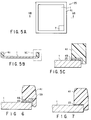
- FIGS. 5A - 5C shows the plan view and the sectional view, and the partially enlarged view thereof of the chip having a chip frame mounted thereon.
- the chip 1 has a planar high voltage structure, and the shape is, for example, square.
- the periphery thereof is coated with a passivation film 23 of polyimide resin.
- a chip frame 41 comprising silicone or engineering plastics formed by a separate process in advance is adhered by an adhesive 49, such as silicone or polyimide (see FIG. 5C).
- This chip frame 41 and the adhesive 49 covers the upper face and side faces of the chip periphery, but does not reach to the back face collector of the chip. Furthermore, the size of the chip frame 41 is such as to keep a distance for preventing surface breakdown according to the voltage rating of the chip 1.
- a standard is a distance of 1 mm or longer per 1 KV. It has such a shape as to guide on the side face of the chip 1, as shown in 5C, for positioning at the time of adhering the chip frame 41 and the chip 1.
- FIG. 6 and FIG. 7 show the modified embodiment of the mounting method of the chip frame.
- a trench 59 is provided on the contact plane of the chip frame 41 with the adhesive 49.
- the adhesive gets in the trench 59 to improve the adhesive strength.
- the chip frame 41 is formed integrally with the chip by using a molding technology of silicone resin and the like.
- a slightly tapered angle is provided in the upper portion of the chip frame, and each corner portion is rounded.
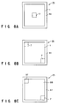
- the gate electrode contacting area G provided on the emitter surface of the chip 1 is shown as 7 on the chip, but in this embodiment, 7 is formed in any corner of four corners of the chip. But the position of this contacting area does not have to be restricted to the corner, and it may be formed in the central region of the chip, as shown in FIG. 8A, or may be formed more than one or two as shown in FIG. 8B.
- the region other than the gate electrode contacting area and the region covered with the chip frame 41 in the peripheral region becomes the contacting area of the emitter electrode, that is, the press-contact region.
- FIG. 8C is a plan view of the IGBT chip used in another example.
- said emitter control electrode 97 is formed at the corner region of the chip, as well as the contacting area 7 of the gate electrode.
- the emitter control electrode 97 is insulated with the main emitter electrode 99 on the chip.
- the emitter control electrode 97 is provided for detecting the overcurrent and designed in such an area ratio that minute current (in the order of 10 mA - 1A) is given with respect to the main emitter electrode 99.
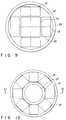
- FIG. 9 is a modification of the ring frame in this embodiment.
- the external frame 29 (the circular ring frame in this embodiment) is composed of the ring portion constituting the outer periphery and the projection 47 extending from the inner wall of the ring portion toward the inside, but a lattice 57 connected integrally to the projection 47 may be formed inside of the ring frame.
- a lattice 57 connected integrally to the projection 47 may be formed inside of the ring frame.
- FIG. 10 is a plan view of the second embodiment of the press-contact type reverse conduction IGBT device
- FIG. 11 is a sectional view of the region along the line XI - XI of FIG. 10.
- a chip with a bevel structure is formed in the hybrid assembly.
- This chip collective body positions each chip of the collective body so as to enclose the outer periphery thereof, and is enclosed by a circular ring frame 29 which protects the periphery thereof.
- the chip collective body is press-contacted by the collector electrode plate 33 which is the first electrode plate and the emitter electrode plate 35 which is the second electrode plate as shown in FIG. 11.
- thermal buffer plates 37 and 39 composed of, for example, molybdenum are inserted. Namely, a collector thermal buffer plate 37 is inserted between the IGBT chips 25 and the FRD chip 27, and the collector electrode plate 33, and between these chips 25 and 27 and the emitter electrode plate 35, emitter thermal buffer plates 39 are inserted. Chips 25 and 27 are arranged and fixed on the collector thermal buffer plate 37.
- the collector thermal buffer plate 37 is composed of a circular portion which supports the FRD chip 27 and a doughnut shaped portion which supports eight chips
- the emitter buffer plate 39 is composed of a circular plate which covers the FRD chip 27 and square eight plates which covers each IGBT chip 25.
- the ring frame 29 fixes the chip collective body so as to enclose the chip collective body from outside by the projection 47 thereof.
- Chip frames 41 composed of silicon resin and the like are mounted to the outer periphery of respective chips 25 and 27. Furthermore, between the emitter thermal buffer plate 39 and chips 25, 27, soft metal thin film 43, such as copper and the like to improve the contact state is inserted.
- the projection 47 of the ring frame 29 is placed on the collector thermal buffer plate 37, with the tip thereof abutting against the chip frame in the chip periphery.
- the chip frame 41 has functions to strengthen the insulation of the chip periphery and to facilitate the arrangement, such as positioning at the time of forming the chip collective body.
- the thickness adjusting plate composed of, for example, a silver sheet.
- a silver sheet 63 is inserted between the emitter electrode plate 35 and the emitter thermal buffer plate 39 on the emitter side, and a silver sheet 65 is inserted between the collector electrode plate 33 and the collector thermal buffer plate 37 on the collector side.
- soft metal sheets are inserted on the outside of the thermal buffer plates as a thickness adjusting plate to adjust the slight difference of the thickness of the chip, soft metal sheets and the thermal buffer plates, and to perform uniform press-contact.
- FIG. 12 is a sectional view of the third embodiment of the press-contact type reverse conduction IGBT device.
- a plurality of square shaped IGBT chips 25 and FRD chips 27 are respectively protected by the chip frames 41.
- the chip collective body is press-contacted by the collector electrode plate 33 which is the first electrode plate and the emitter electrode plate 35 which is the second electrode plate.
- thermal buffer plates 37 and 39 composed of, for example, molybdenum are inserted. Namely, a collector thermal buffer plate 37 is inserted between the IGBT chips 25 and the FRD chips 27, and the collector electrode plate 33, and between these chips 25 and 27 and the emitter electrode plate 35, emitter thermal buffer plates 39 are inserted.
- Chips 25 and 27 are arranged and fixed on the collector thermal buffer plate 37.
- the emitter thermal buffer plate 39 is composed of a square shaped plate which press-contacts each chip, respectively.
- the ring frame 29 fixes the chip collective body so as to enclose the chip collective body from outside by the projection 47 thereof.
- soft metal thin films 43 such as copper and the like to improve the contact state are inserted.
- the projection 47 of the ring frame 29 is placed on the collector thermal buffer plate 37, with the tip thereof abutting against the chip frame 41 in the chip periphery.
- the chip frame 41 has functions to strengthen the insulation of the chip periphery and to facilitate the arrangement, such as positioning at the time of forming the chip collective body.
- the thickness adjusting plate composed of, for example, a silver sheet.
- a silver sheet 63 is inserted between the emitter electrode plate 35 and the emitter thermal buffer plate 39 on the emitter side, and a silver sheet 65 is inserted between the collector electrode plate 33 and the collector thermal buffer plate 37 on the collector side.
- soft metal sheets are inserted on the outside of the thermal buffer plates as a thickness adjusting plate to adjust the slight difference of the thickness of the chip, soft metal sheets and the thermal buffer plates, and to perform uniform press-contact.
- This buffer plate has also a function to adjust the difference of the thickness between chips, to some extent.
- trenches 67 and 69 are formed on the inner surface facing to the chips of the collector electrode plate 33 and the emitter electrode plate 35.
- the trenches are formed so as to be located between chips, considering the size of the chip.
- the region facing to the chip of the emitter electrode plate enclosed with said trench has a characteristic that it is smaller than the area of the thermal buffer plate 39 intervened between the chips. Thus, it can prevent the load concentration of the IGBT chips 25 and FRD chips 27 to the chip periphery, at the time of press-contact, thereby the concentration of the stress to the chip peripheral region can be released.
- a gate lead 45 is press-contacted by a spring.
- the one end of the gate lead 45 is guided to the outside of the outer peripheral device 51 through the metal sleeve 55 which is silver-soldered to the side wall of the cylindrical outer peripheral device 51.
- a seal is provided to the metal sleeve 55 to seal the chips 25 and 27 within the outer peripheral device 51.
- trenches 67 and 69 are provided in the collector electrode plate 33 and the emitter electrode plate 35 in said third embodiment, in this embodiment, as shown in FIG. 13, only one trench 69 of the emitter electrode plate is provided, and the thickness of the collector thermal buffer plate 37 is largely increased.
- the thermal buffer plate has also the function to adjust the difference in thickness between chips, by making it thicker, the copper thin film 43 for improving the contact state of the emitter thermal buffer plate and the chip which is required in the third embodiment, and the silver sheets 63 and 65 which adjust the thickness between the emitter and collector electrode plates and the thermal buffer plate are removed to simplify the structure of the device.
- a gate probe mounted to the gate electrode region 101 of the trench is connected to the gate electrode contacting area 7 (see FIG. 8A) provided in the central region of the IGBT chip 25, which is guided to outside through the trench 69 by the gate lead 45 connected to the probe.
- FIGS. 14 - 16 are modifications of the emitter electrode plate 35 having the trenches 69.
- trenches 69 are formed lengthwise and crosswise on the inner surface of the emitter electrode plate, and said gate lead 45 can be set in these trenches.
- high functionality of the device can be obtained easily by embedding other leads such as the emitter control lead and the like (see FIG. 8C), and the temperature detecting thermistor and the like.
- sufficient trenches are formed preliminarily, and only necessary ones are used for wiring of the lead.
- gate electrode regions 101 corresponding to the gate electrode contacting areas 7 on the IGBT chips are formed.
- the gate electrode regions 101 are not used with respect to FRD chips.
- the square shaped flat region enclosed by these trenches are used as the press-contact plane.
- FIG. 15 shows the embodiment in which the trenches are formed, on the contrary, in the emitter electrode plate, only in the portions necessary for wiring of the lead and the like. If there is a necessity to arrange other leads and a thermistor, trenches for them are further formed. 8 is opposite to the gate electrode contacting area 7 on the chip. In this embodiment, as shown in FIG. 5A, a case where 7 is provided at the corner of the IGBT chip is shown.
- FIG. 16 is other modification of the emitter electrode plate.
- trenches 69 are formed lengthwise and crosswise on the inner surface of the emitter electrode plate, but the gate electrode region of the trench is provided at the corner of the press-contact plane to the IGBT chip, and IGBT chips are arranged in the peripheral region of the electrode plate and FRD chip is arranged in the central region thereof.
- the trench portions are opposite to the chip frame-forming region of the chip periphery, and it does not contribute to the heat release, therefore, it hardly gives the influence to the heat release characteristic of the whole press contact device.
- the emitter electrode plate shown in FIGS. 14 - 16 can be applied to the third embodiment other than this embodiment.
- FIG. 17 is a sectional view of the stud type reverse conduction IGBT semiconductor device having a rating of 600V - 800A
- FIG. 18 is a plan view of the base used for this semiconductor device
- FIG. 19 is a plan view of the semiconductor device showing the arrangement of the chips
- FIG. 20 is a plan view showing the inside of the ceramic cap used for the semiconductor device
- FIG. 21 is a sectional view showing the using state of the plate spring within the device.
- an insulating substrate 105 of aluminum nitride and the like is mounted to the base 103, and a collector electrode plate 33 composed of copper having a thickness of about 0.5 mm, which is the first electrode plate, is mounted to 105, and IGBT chip 25 and FRD chip 27 are placed thereon.
- the periphery of each chip is protected by the chip frame 41 of silicone resin and the like, as shown in FIG. 18.
- Buffer plates 39 of molybdenum are placed on the chips, and a common emitter electrode plate 35 having a thickness of about 0.5 mm thereon pressurizes all buffer plates 39 of the chips.
- a cylindrical outer peripheral device 51 placed on the base 103 encloses these chips, and is sealed by a ceramic cap 75.
- the emitter external electrode E, collector external electrode C, gate external electrode G and emitter control external electrode S of this semiconductor device are supported by the ceramic cap 75.
- the emitter external electrode E is connected to the emitter electrode plate 35 via the emitter electrode post 77 mounted on one chip among IGBT chips 25 and FRD chips 27 and the strand wire 79.
- Both side probes or springs placed in the insulator tube 81 on the chip connect the gate external electrode G and the gate electrode formed on the surface of IGBT chips 25. Connection between gate electrodes of IGBT chips 25 is performed by using the metallized pattern formed on the inner surface of the ceramic cap 75.
- the emitter electrode plate 35 connects between the emitters of respective chips into one.
- the collector external electrode C is electrically connected to the common collector electrode plate 33.
- a FRD chip 27 since the central chip in FIG. 17 is, as shown in the plan view of FIG. 19, a FRD chip 27, a probe is not inserted to the insulator tube shown in FIG. 17 and the insulator tube becomes hollow.
- the press contact to the chips by the emitter electrode plate 35 is energized by the plate spring 83 mounted on each chip via a washer 85.
- the emitter control external electrode S is directly connected to the emitter control electrode on the chip, via an emitter control lead 95 of a probe and the like, thereby the parasitic resistance can be reduced.
- the collector external electrode C and the emitter external electrode E are connected by caulking or soldering the external trip terminal, respectively. These external trip terminals are mounted vertically, but they may be mounted horizontally.
- FIG. 18 is a plan view of the base 103.
- the base 103 has a mounting hole, and is composed of supporting portions 71 of copper loaded with respective chips and a lattice portion 73 of iron supporting this supporting portions 71. Since copper is readily deformed, and expands outwardly due to the internal press-contact force, and thereby the press-contact force does not applied or the uniformity is harmed, the lattice 73 of iron is added to surround it, as in this embodiment, to increase the strength of the base.
- the supporting portion 71 of copper is disposed only under the chip.
- An outer peripheral device 51 is formed in the periphery of the base 103.
- FIG. 19 is a plan view showing the inside of the outer peripheral device 51.
- FIG. 17 is a sectional view of the region along the line XVII - XVII.
- the chips arranged therein are composed of four IGBT chips 25 and two FRD chips 27 in the central region. Plate springs 83 to press-contact the chip are formed on the respective chips.
- the emitter external electrode E is formed on one of FRD chips 27, and the collector external electrode C is formed in a given space.
- FIG. 20 is a plan view showing the surface facing to the inside of the outer peripheral device 51 of the ceramic cap 75 shown in FIG. 17.
- a metallized pattern 87 of the gate electrode is formed on this surface.
- Blank portions F and H are formed in order to connect a resistor, a condenser, Zener diode and the like by soft soldering or silver soldering at some portions in the metallized pattern 87. If there is no need to attach these parts, these blank portions may be metallized.
- This metallized pattern 87 connects between gates of IGBT chips 25.
- To the blank portion F for example, a condenser and Zener diode are connected.
- To the blank portion H for example, a resistor is connected.
- FIG. 21 is an enlarged view showing the structure of the plate spring. Plate springs are attached to every chip, thereby the difference in grade of the thickness per every chip can be readily adjusted by its stroke.
- FIGS. 22 - 24 are plan views and sectional views of modifications of the chip frame mounted to the chip.
- IGBT chips 25 are composed of a silicon chip 1 and a chip frame 41 which covers and protects the peripheral region of the chip.
- the surface of the chip 1 has a contacting area 7 of the gate electrode and a press-contact region of the emitter electrode exposed from the chip frame.
- the chip frame 41 has an extending portion 89 and this extending portion 89 covers the contacting area 7 of the gate electrode on the surface of the chip. By the existence of this extending portion 89, the chip frame 41 has a function to support the gate lead 45.
- FIG. 22A is a plan view when the contacting area of the tip of the gate lead comprises a socket and a probe
- FIG. 22B is a sectional view along the line XXIIB - XXIIB thereof.
- the tip of the probe is joined to the contacting area 7 of the gate electrode of the chip 1 through a circular breakthrough in the extending portion 89.
- the contacting area of the tip of the gate lead 45 comprises a spring pin, and the gate lead 45 is fitted into the kerf in the extending portion 89, and the tip of the spring pin is joined to the contacting area 7 of the gate electrode.
- FIG. 23B the contacting area of the tip of the gate lead 45 comprises a spring pin, and the gate lead 45 is fitted into the kerf in the extending portion 89, and the tip of the spring pin is joined to the contacting area 7 of the gate electrode.
- the contacting area of the tip of the gate lead 45 comprises a socket and an embedded spring pin, and this spring pin is joined to the contacting area 7 of the gate electrode on the surface of the chip 1, through the breakthrough having a rectangle section in the extending portion 89 shown in FIG. 24A.
- FIG. 25 is shown collectively a structure of various gate leads 45 connecting the gate terminal G guided to the outside of the semiconductor device and the gate electrode of each IGBT chip.
- the gate terminal is formed by combining a plurality of gate leads 45 connected from a plurality of chips.
- an oscillation-preventing resistor may be wired to the gate lead 45.
- the resistor is preferably placed in the vicinity of the chip as near as possible so as to reduce the L component.
- the resistor is covered with an insulation-coated tube.
- the connecting methods of the gate lead 45 and the gate electrode 7 of the chip include the methods shown in FIGS. 22 - 24.
- the socket is fitted to the probe, a spring pin or the like of the gate electrode.
- a Zener diode having a breakdown voltage of about 30V for preventing overvoltage of the gate may be inserted between the gate and the emitter.
- a condenser may be inserted between the gate and the emitter.
- FIG. 26A is a plan view of the emitter thermal buffer plate 39 and a sectional view along the line XXVIB - XXVIB thereof.
- the molybdenum plate used for the emitter thermal buffer plate 39 has a thickness of about 1 - 2 mm, and the four corners are processed to the radius of curvature R of about 0.2 - 1 mm. This processing is performed by punching followed by barrel finishing, and the load concentration to the corner portions is released. Since this buffer plate 39 has a gate lead breakthrough 93 formed in the central region thereof, it is used for the IGBT chip in which the contacting area of the gate electrode is formed in the central region. Said radius of curvature R is applied to the breakthrough 93. This processing has the same effect to the soft metal thin film of copper and the like.
- the chip frame 41 is adhered to the side face and the surface on the emitter side of the chip 1, and at this time, the corner of the lower portion of the inner side wall of the frame to be adhered is subjected to chamfering in about 0.2 mm.
- An adhesive 49 is applied to the contact plane of the chip frame 41 thereafter, and both of them are adhered. By such processing, exudation of the adhesive 49 to the pattern on the chip surface can be prevented.
- the external frame which integrally protects the collective body of the chip is a disk-like form, and is called a ring frame, but the present invention is not restricted to this shape. As shown in FIG. 28, there is a semiconductor device having a square shape, and in this case, also the external frame 29 becomes square. Since the chip collective body is almost square, it becomes more compact than the one having a circular shape.
- FIGS. 29A, 29B and 29C show the method to attach a thermistor to the trench of the electrode plate for wiring the gate lead.
- the thermistor is used for detection of the temperature of the chip.
- an exclusive trench 91 (not shown in FIG. 15) is prepared, and when the electrode plate of FIG. 14 and FIG. 16 is used, the necessary trench is selected.
- a trench 91 for forming a circuit of the temperature detecting element (thermistor) is formed in the electrode plate 35, for example, shown in FIG. 15, and is fixed by a silicone rubber by embedding a thermistor.
- the multi-chip press-contact type high speed power device in which various kinds of multiple chips of the present invention are arranged in high density has characteristics described below:
- the high speed power device having a planar high voltage structure which has been impossible to press-contact in the conventional press-contact structure is made possible by mounting a chip frame of synthetic resin at the chip periphery. Furthermore, by fixing the collective body of the chip by an external frame, various kinds of chips such as IGBT chips, FRD chips and the like can be collectively press-contacted. Moreover, difference at the time of collective press contact due to the difference of the chips and the thickness of members can be suppressed and uniform press contact is made possible by inserting a thickness adjusting plate of a soft metal sheet and making the thickness of the thermal buffer plate sufficiently thick.
Landscapes
- Engineering & Computer Science (AREA)
- Power Engineering (AREA)
- Microelectronics & Electronic Packaging (AREA)
- Computer Hardware Design (AREA)
- Physics & Mathematics (AREA)
- Condensed Matter Physics & Semiconductors (AREA)
- General Physics & Mathematics (AREA)
- Ceramic Engineering (AREA)
- Die Bonding (AREA)
- Thyristors (AREA)
Abstract
Description
- The present invention relates to a press-contact type semiconductor device, more particularly, relates to MOS gate drive switching devices such as IGBT (Insulated Gate Bipolar Transistor) having a plurality of semiconductor substrates.
- Conventionally, the structure of the press-contact type semiconductor device has been only one which press-contacts a single semiconductor substrate (hereinafter referred to as "chip"). For example, in the press-contact type device of the anode short type GTO (Gate Turn-Off) thyristor, the disc type chip includes N-type emitter layer, P-type base layer, N-type base layer and P-type emitter layer, from the chip surface which is the cathode toward the back face of the chip which is the anode.
- N-type emitter region on the chip surface is formed as a plurality of mesas on P-type base layer. These N-type emitter regions has an aluminum cathode electrode on the top portion of said mesas, and a plurality of gate electrodes composed of aluminum are provided in P-type base layer exposed by said mesa processing. On the back face of the chip, a plurality of P-type emitter regions having a planar structure are formed within the surface of a flat N-type base layer, and the anode short type GTO thyristor is formed by providing the anode electrode composed of aluminum on the whole face thereof, extending over said N-type base layer and P-type emitter regions. The side face of the chip is coated with, for example, silicone resin for the insulation protection.
- On the cathode electrode of the top portion of said mesas, the cathode external electrode is press-contacted, and on the anode electrode, the anode external electrode is press-contacted. The above-mentioned press-contact type device of the anode short type GTO thyristor is disclosed in KOUKAI, "Press-contact type semiconductor device", HEI, 4-137561 (12 May, 1992).
- Recently, IGBT has appeared as a MOS gate drive type switching device. This device is characterized in that it has an advantage that it makes high voltage and high current operation easy, which the bipolar transistor has, and an advantage that driving is easy. As the switching device using this IGBT, a RC (Reverse Conduction) type switching device incorporating FRD (Free Wheel Diode) is known. This device is the one which connects FRD to IGBT in inversely parallel, and used in a module structure. This module is assembled by forming an electrode pattern used as given collector electrode, emitter electrode, emitter control electrode and gate electrode on the insulation substrate, and by solder mounting a plurality of IGBT back-face collectors and FRD chips, respectively, on said collector electrode pattern. The emitter on the upper face of the chip, emitter control and respective electrodes of the gate, and the corresponding electrode patterns on the insulation substrate are connected by a bonding wire, respectively.
- The surface of IGBT chip mounted on the switching device of this module structure is coated with a passivation film such as polyimide, except for the bonding pad of the gate and emitter. The square shaped silicon chip of IGBT forms the collector electrode of the metal multilayer film over the whole surface of the back face of the chip in order to facilitate soldering.
- For example, since the press-contact type semiconductor device composed of the conventional GTO thyristor has only one structure to press-contact one chip, there are defects described below:
- (1) High current operation of the element is difficult. Namely, in order to increase the current rating of the element, it has been necessary to make the chip size large. However, if the chip size is increased, such problems are caused that in the high-speed power element such as MOS gate type switching devices of IGBT, the possibility to contain unrestorable defects which make fine processing difficult is increased to increase the failure rate.
- (2) Highly functionalizing and high value-adding are difficult. For example, when RC type IGBT device is produced, two different kinds of device structures, IGBT and FRD have to be produced in one wafer, thereby the production process is complicated and production becomes difficult.
- Furthermore, when the conventional module type semiconductor device is used to be mounted on a vehicle (for traction applications), such problems described below are caused:
- (1) Reliability for the power cycle of bonding
It is required that semiconductor devices for traction applications have to be endurable to the power cycle of 6 million cycles at a temperature variation of 25°C, but in the current technology, it can only endure 3 million cycles. - (2) Reliability for the thermal fatigue of the soldering layer
It is required that the soldering layer has to be endurable, as in said bonding, to the power cycle of 75,000 cycles at a temperature variation of 70°C, but in the current technology, it can only endure about 25,000 cycles. - (3) Reliability for cooling of the element
Conventional module type semiconductor devices are cooled on the only one face from the collector side, and cooling from the emitter electrode side is almost impossible. Therefore, in order to enhance the heat dissipation, the outside diameter of the element has to be increased. For example, in the RC type IGBT module of 1200A - 2500V class, the outside diameter becomes 130 × 260 × 40 mm. - (4) Reliability for high temperature operation
In semiconductor devices for traction applications, the operating temperature in use is had to be insured in the range of -40°C - 150°C, but the resin of the case material is not endurable against such temperature. - (5) Reliability for high voltage operation
Since the case material is a resin and easy to cause tracking, it is not endurable against high voltage operation. - (6) Reliability for wiring
Since wiring within the module is fine and complicated, there are such problems as noise generation in the gate circuit due to the wiring inductance, and generation of the spike voltage at the time of diode recovery. - The present invention has been completed under this background. It is therefore the object of the present invention to provide MOS gate drive type, planar switching devices having high reliability and suitable for traction and industrial applications, by giving a press-contact structure to the multi-chip type device.
- The present invention is characterized in that a chip frame made of a synthetic resin is mounted to each periphery of multiple semiconductor chips containing MOS gate drive type chips, each chip is arranged on the same plane so as to abut against the chip frame thereof, and these are press-contacted and secured by the first electrode plate and the second electrode plate. Furthermore, by regulating the outer periphery of the arranged multiple semiconductor chips using the external frame inserted between the first electrode plate and the second electrode plate, each chip is positioned.
- Namely, the press-contact type semiconductor devices of the present invention include multiple semiconductor chips (hereinafter referred to as "semiconductor substrate"), the periphery of which being enclosed by the chip frame of insulating resin, a first electrode plate and a second electrode plate, the semiconductor substrate being arranged on the same plane so as to abut against the chip frame with each other, wherein the semiconductor substrate arranged on the same plane is press-contacted from the upper and the lower sides by the first electrode plate and the second electrode plate.
- Furthermore, it may be so constituted that between the first electrode plate and the second electrode plate, an external frame of insulating resin is mounted such that this external frame has a circular body enclosing the side faces of the first and second electrode plates, and a projection spreading from the inner wall to the inside of this circular body (for example, see 47 in FIGS. 1 and 2), the multiple semiconductor substrates arranged on the same plane being enclosed by this projection to make the chip frames abut with each other, subsequently being press-contacted by the first and second electrode plates.
- Between the first electrode plate or second electrode plate, or the first and second electrode plates, and the semiconductor substrate, a thermal buffer plate may be intervened. Or, a thickness adjusting plate composed of a soft metal sheet may be intervened so as to abut against the press-contact plane of the first electrode plate or second electrode plate, or the first and second electrode plates. On the press-contact plane of the first electrode plate or second electrode plate, or the first and second electrode plates, a trench may be formed in the periphery of the predetermined portion opposite to the semiconductor substrate to apply the stress at the time of press-contact uniformly to the chip. Though a gate electrode contacting area is formed in a part of the emitter surface of the semiconductor substrate, the chip frame has an extending portion extending from the upper edge corner of the frame to inside thereof, the extending portion covering the gate electrode contacting area, where probes connected with the gate electrode may be provided.
- The chip frame of a synthetic resin mounted to the periphery of respective chips plays a role as a positioning guide as well as protecting the insulation of the periphery, to make it possible to fix the chips and the press-contact plate at a minimum size. The external frame enclosing the outer periphery of the chip frame arranges the chip frames accurately, and enabling to determine the positional relation of the gate electrode accurately, and arrange the chips in high density. Moreover, the thickness-adjusting plate composed of a soft metal sheet having ductility, such as silver, which is inserted between the chip and the electrode plate enables to uniformly press-contact chips having different thickness. The thermal buffer plate releases the thermal stress of the semiconductor device, and the trench formed on the press-contact plane of the electrode plate releases the stress concentration to the chip periphery. The extending portion of the chip frame covering the contacting area of the gate electrode facilitates the connection to the contacting area of the gate lead, while protecting the contacting area.
- This invention can be more fully understood from the following detailed description when taken in conjunction with the accompanying drawings, in which:
- FIG. 1 is a plan view of the semiconductor device in the first embodiment of the present invention;
- FIG. 2 is a sectional view of a region along the line II - II of FIG. 1;
- FIG. 3 is a sectional view of the peripheral region of the semiconductor substrate;
- FIG. 4 is a sectional view of the central region of the semiconductor substrate;
- FIG. 5A is a first plan view of the semiconductor substrate;
- FIG. 5B is a sectional view along the line VB - VB of the semiconductor substrate;
- FIG. 5C is a first enlarged sectional view in the region VC of FIG. 5B;
- FIG. 6 is a second enlarged sectional view in the region VC of FIG. 5B;
- FIG. 7 is a third enlarged sectional view in the region VC of FIG. 5B;
- FIG. 8A is a second plan view of the semiconductor substrate;
- FIG. 8B is a third plan view of the semiconductor substrate;
- FIG. 8C is a fourth plan view of the semiconductor substrate;
- FIG. 9 is a plan view of a modified embodiment of the semiconductor device shown in FIG. 1;
- FIG. 10 is a plan view of the semiconductor device in the second embodiment of the present invention;
- FIG. 11 is a sectional view of a region along the line XI - XI of FIG. 10;
- FIG. 12 is a sectional view of a region in the third embodiment;
- FIG. 13 is a sectional view of a region in the fourth embodiment;
- FIG. 14 is a first plan view of an emitter electrode plate;
- FIG. 15 is a second plan view of an emitter electrode plate;
- FIG. 16 is a third plan view of an emitter electrode plate;
- FIG. 17 is a sectional view of the semiconductor device in the fifth embodiment;
- FIG. 18 is a plan view of the base of the semiconductor device shown in FIG. 17;
- FIG. 19 is a plan view of the chip arrangement of the semiconductor device shown in FIG. 17;
- FIG. 20 is a plan view of the ceramic cap of the semiconductor device shown in FIG. 17;
- FIG. 21 is a sectional view of the plate spring of the semiconductor device shown in FIG. 17;
- FIG. 22A is a fifth plan view of the semiconductor substrate;
- FIG. 22B is a sectional view of a region along XXIIB - XXIIB of FIG. 22A;
- FIG. 23A is a sixth plan view of the semiconductor substrate;
- FIG. 23B is a sectional view of a region along XXIIIB - XXIIIB of FIG. 23A;
- FIG. 24A is a seventh plan view of the semiconductor substrate;
- FIG. 24B is a sectional view of a region along XXIVB - XXIVB of FIG. 24A;
- FIG. 25 is a view of various gate leads connected to the gate terminal of the semiconductor device of the present invention;
- FIG. 26A is a plan view of the buffer plate used for the semiconductor device of the present invention;
- FIG. 26B is a sectional view of a region along XXVIB - XXVIB of FIG. 26A;
- FIG. 27 is a sectional view illustrating the way to mount the chip frame of the semiconductor device of the present invention;
- FIG. 28 is a plan view of a square shaped external frame of the semiconductor device of the present invention;
- FIG. 29A is a first sectional view of a thermistor mounted to the trench of the electrode plate of the present invention;
- FIG. 29B is a second sectional view of a thermistor mounted to the trench of the electrode plate of the present invention; and
- FIG. 29C is an example to mount the thermistor to the gate lead.
- Embodiments of the present invention will now be described with reference to the accompanied drawings.
- The first embodiment will be described with reference to FIGS. 1 to 9. FIG. 1 is a schematic plan view of the press-contact type reverse conduction IGBT device, FIG. 2 is a sectional view of the region along the line II - II thereof, FIGS. 5A, 5B and 5C are a plan view and sectional views of the IGBT chip mounted with a chip frame, and FIGS. 6 to 9 are modified embodiments of respective regions of the present embodiment. As shown in FIG. 1, this device is composed of nine
IGBT chips 25 in the central region and twelveFRD chips 27 in the peripheral region. Respective chips are square, but the collective body collecting them is press-contacted to the circular form. This chip collective body is enclosed by theexternal frame 29 which protects the outer periphery thereof and is positioned. Since the planar shape of the device of this embodiment is circular, theexternal frame 29 enclosing the chip collective body becomes also circular. This external frame is referred to as a ring frame. As shown in FIG. 2, this chip collective body is press-contacted by thecollector electrode plate 33 which is the first electrode plate and theemitter electrode plate 35 which is the second electrode plate, but between the electrode plate and the chip,thermal buffer plates - Namely, a collector
thermal buffer plate 37 is inserted between theIGBT chip 25 andFRD chip 27, and thecollector electrode plate 33, and an emitterthermal buffer plate 39 is inserted between thesechips emitter electrode plate 35.Chips thermal buffer plate 37. These chips are lined up leaving no space therebetween on the collector thermal buffer molybdenum plate, and fixed by thering frame 29 which guides so as to enclose from outside. Chip frames 41 composed of silicone resin etc. are attached to the outer periphery ofrespective chips thermal buffer plate 39 and thechips thin film 43 composed of, for example, copper is inserted in order to improve the contact state. - The
ring frame 29 has aprojection 47 extending from the inner wall to the inside, and positions chips so as to enclose the outer periphery of the arranged chip collective body. The tip of theprojection 47 of thering frame 29 abuts against thechip frame 41 on the chip periphery, and placed on the collectorthermal buffer plate 37. Thechip frame 41 has a function to facilitate the positioning when the chip collective body is formed, as well as to strengthen insulation of the peripheral region. - In this embodiment, the example of the press-contact type reverse conduction IGBT device provided with IGBT element having 9 chips and FRD element having 12 chips is shown, but by using the same chips and changing the numbers and the allocating ratio, devices having various ratings can be provided. As in this embodiment, by making the FRD element square with the same size with respect to IGBT element, the productivity can be improved by standardization of the chip design and the degree of freedom of the assembly technique of the chip frame can be improved. Furthermore, by making the inner wall of the chip frame 41 a guide, the emitter
thermal buffer plate 39 is put on thechips - Next, with reference to FIG. 3 and FIG. 4, the IGBT chip will be described. Both figures are sectional views of the IGBT chip. The emitter surface formed on the upper face of the IGBT chip is covered with a
passivation film 23 of, for example, polyimide except for the power supply region to the gate which is the control electrode and the region abutting against the emitter thermal buffer plate of the emitter electrode. Thispassivation film 23 is formed on the chip periphery, which means to be formed under thechip frame 41 mounted to the chip periphery. FIG. 3 shows the structure of the chip periphery and FIG. 4 shows a given section inside of the chip. - The square shaped
chip 1 includes P-type collector region 13, N-base region 11,P+ base region 15, P-type base region 17, and N-type emitter region 9. P-type collector region 13 is formed on the back face of thechip 1, and on this back face, acollector electrode 22 of, for example, aluminum is formed on the whole face thereof.P+ base region 15 and P-type base region 17 are formed in N-base region 11, facing on the upper face (hereinafter referred to as "emitter surface") of thechip 1. N-type emitter region 9 is formed in P-type base region 17, facing on the emitter surface of thechip 1.Emitter electrode 21 composed of aluminum is formed on N-type emitter region 9, short-circuited to P-type base region 17. On the P-type base region 17 and the N-base region 11 sandwiched between these P-type base regions 17, apolysilicon gate 5 is formed via thegate oxide film 19.Polysilicon gate 5 is coated with aninterlayer insulation film 3 such as a silicon dioxide film, and theemitter electrode 21 is disposed thereon. Thegate electrode 31 connected to thepolysilicon gate 5 is composed of aluminum and the like, and connected to thispolysilicon gate 5 via an opening of the interlaminar film 3 (see FIG. 4). The emitter surface of thechip 1 is coated with apassivation film 23 such as polyimide, except for the contacting area G (not shown) of thegate electrode 31 and the contacting area of theemitter electrode 21. Therefore, the region except for the contacting area G of thegate electrode 31 is coated with apassivation film 23. Thegate electrode 31 is coated and protected with asilicon dioxide film 53, and thepassivation film 23 is formed thereon. - Next, the way to mount the chip frame to IGBT
chip 25 will be described with reference to FIGS. 5 - 8. FIGS. 5A - 5C shows the plan view and the sectional view, and the partially enlarged view thereof of the chip having a chip frame mounted thereon. Thechip 1 has a planar high voltage structure, and the shape is, for example, square. The periphery thereof is coated with apassivation film 23 of polyimide resin. On thepassivation film 23 of polyimide of the periphery, achip frame 41 comprising silicone or engineering plastics formed by a separate process in advance is adhered by an adhesive 49, such as silicone or polyimide (see FIG. 5C). Thischip frame 41 and the adhesive 49 covers the upper face and side faces of the chip periphery, but does not reach to the back face collector of the chip. Furthermore, the size of thechip frame 41 is such as to keep a distance for preventing surface breakdown according to the voltage rating of thechip 1. A standard is a distance of 1 mm or longer per 1 KV. It has such a shape as to guide on the side face of thechip 1, as shown in 5C, for positioning at the time of adhering thechip frame 41 and thechip 1. - FIG. 6 and FIG. 7 show the modified embodiment of the mounting method of the chip frame. In FIG. 6, in order to prevent a shortage of the adhesive, a
trench 59 is provided on the contact plane of thechip frame 41 with the adhesive 49. Thus, the adhesive gets in thetrench 59 to improve the adhesive strength. In FIG. 7, thechip frame 41 is formed integrally with the chip by using a molding technology of silicone resin and the like. Furthermore, in FIG. 6 and FIG. 7, a slightly tapered angle is provided in the upper portion of the chip frame, and each corner portion is rounded. By such finishing processing, the operation described above to arrange the chip frame by using the ring frame and to position the chip collective body can be done quite smoothly. - In FIG. 5A, the gate electrode contacting area G provided on the emitter surface of the
chip 1 is shown as 7 on the chip, but in this embodiment, 7 is formed in any corner of four corners of the chip. But the position of this contacting area does not have to be restricted to the corner, and it may be formed in the central region of the chip, as shown in FIG. 8A, or may be formed more than one or two as shown in FIG. 8B. The region other than the gate electrode contacting area and the region covered with thechip frame 41 in the peripheral region becomes the contacting area of the emitter electrode, that is, the press-contact region. - FIG. 8C is a plan view of the IGBT chip used in another example. On the emitter surface, said
emitter control electrode 97 is formed at the corner region of the chip, as well as the contactingarea 7 of the gate electrode. Theemitter control electrode 97 is insulated with themain emitter electrode 99 on the chip. Theemitter control electrode 97 is provided for detecting the overcurrent and designed in such an area ratio that minute current (in the order of 10 mA - 1A) is given with respect to themain emitter electrode 99. - FIG. 9 is a modification of the ring frame in this embodiment. In the embodiment shown in FIG. 1, the external frame 29 (the circular ring frame in this embodiment) is composed of the ring portion constituting the outer periphery and the
projection 47 extending from the inner wall of the ring portion toward the inside, but alattice 57 connected integrally to theprojection 47 may be formed inside of the ring frame. When the number of chips becomes large and the sum of each dimensional tolerance comes off the positioning accuracy, adequate introduction of such lattice can help the positioning operation of the chip collective body to obtain the best effect. - Next, the second embodiment will be described with reference to FIGS. 10 and 11.
- FIG. 10 is a plan view of the second embodiment of the press-contact type reverse conduction IGBT device, and FIG. 11 is a sectional view of the region along the line XI - XI of FIG. 10. In this embodiment, a chip with a bevel structure is formed in the hybrid assembly. As shown in FIG. 10, there are arranged one
circular FRD chip 27 in the bevel structure, and 8square IGBT chips 25 in the periphery thereof. This chip collective body positions each chip of the collective body so as to enclose the outer periphery thereof, and is enclosed by acircular ring frame 29 which protects the periphery thereof. The chip collective body is press-contacted by thecollector electrode plate 33 which is the first electrode plate and theemitter electrode plate 35 which is the second electrode plate as shown in FIG. 11. Between the electrode plate and the chips,thermal buffer plates thermal buffer plate 37 is inserted between the IGBT chips 25 and theFRD chip 27, and thecollector electrode plate 33, and between thesechips emitter electrode plate 35, emitterthermal buffer plates 39 are inserted.Chips thermal buffer plate 37. Though in the first embodiment, these chips are lined up leaving no space therebetween on the collector thermal buffer plate, in this embodiment, the collectorthermal buffer plate 37 is composed of a circular portion which supports theFRD chip 27 and a doughnut shaped portion which supports eight chips, and theemitter buffer plate 39 is composed of a circular plate which covers theFRD chip 27 and square eight plates which covers eachIGBT chip 25. - The
ring frame 29 fixes the chip collective body so as to enclose the chip collective body from outside by theprojection 47 thereof. Chip frames 41 composed of silicon resin and the like are mounted to the outer periphery ofrespective chips thermal buffer plate 39 andchips thin film 43, such as copper and the like to improve the contact state is inserted. Theprojection 47 of thering frame 29 is placed on the collectorthermal buffer plate 37, with the tip thereof abutting against the chip frame in the chip periphery. Thechip frame 41 has functions to strengthen the insulation of the chip periphery and to facilitate the arrangement, such as positioning at the time of forming the chip collective body. - Furthermore, in this embodiment, it is so controlled that the chips are uniformly press-contacted by using the thickness adjusting plate composed of, for example, a silver sheet. Namely, a
silver sheet 63 is inserted between theemitter electrode plate 35 and the emitterthermal buffer plate 39 on the emitter side, and asilver sheet 65 is inserted between thecollector electrode plate 33 and the collectorthermal buffer plate 37 on the collector side. Thus, soft metal sheets are inserted on the outside of the thermal buffer plates as a thickness adjusting plate to adjust the slight difference of the thickness of the chip, soft metal sheets and the thermal buffer plates, and to perform uniform press-contact. - Next, the third embodiment will be described with reference to FIG. 12.
- FIG. 12 is a sectional view of the third embodiment of the press-contact type reverse conduction IGBT device. A plurality of square shaped
IGBT chips 25 andFRD chips 27 are respectively protected by the chip frames 41. The chip collective body is press-contacted by thecollector electrode plate 33 which is the first electrode plate and theemitter electrode plate 35 which is the second electrode plate. Between the electrode plate and the chips,thermal buffer plates thermal buffer plate 37 is inserted between the IGBT chips 25 and the FRD chips 27, and thecollector electrode plate 33, and between thesechips emitter electrode plate 35, emitterthermal buffer plates 39 are inserted.Chips thermal buffer plate 37. These chips are lined up leaving no space therebetween on the collector thermal buffer plate, and the emitterthermal buffer plate 39 is composed of a square shaped plate which press-contacts each chip, respectively. Thering frame 29 fixes the chip collective body so as to enclose the chip collective body from outside by theprojection 47 thereof. Between the emitterthermal buffer plate 39 andchips thin films 43, such as copper and the like to improve the contact state are inserted. Theprojection 47 of thering frame 29 is placed on the collectorthermal buffer plate 37, with the tip thereof abutting against thechip frame 41 in the chip periphery. Thechip frame 41 has functions to strengthen the insulation of the chip periphery and to facilitate the arrangement, such as positioning at the time of forming the chip collective body. - Furthermore, in this embodiment, it is so controlled that the chips are uniformly press-contacted by using the thickness adjusting plate composed of, for example, a silver sheet. Namely, a
silver sheet 63 is inserted between theemitter electrode plate 35 and the emitterthermal buffer plate 39 on the emitter side, and asilver sheet 65 is inserted between thecollector electrode plate 33 and the collectorthermal buffer plate 37 on the collector side. Thus, soft metal sheets are inserted on the outside of the thermal buffer plates as a thickness adjusting plate to adjust the slight difference of the thickness of the chip, soft metal sheets and the thermal buffer plates, and to perform uniform press-contact. This buffer plate has also a function to adjust the difference of the thickness between chips, to some extent. Furthermore, in this embodiment,trenches collector electrode plate 33 and theemitter electrode plate 35. The trenches are formed so as to be located between chips, considering the size of the chip. The region facing to the chip of the emitter electrode plate enclosed with said trench has a characteristic that it is smaller than the area of thethermal buffer plate 39 intervened between the chips. Thus, it can prevent the load concentration of the IGBT chips 25 andFRD chips 27 to the chip periphery, at the time of press-contact, thereby the concentration of the stress to the chip peripheral region can be released. - To the gate electrode (not shown), a
gate lead 45 is press-contacted by a spring. The one end of thegate lead 45 is guided to the outside of the outerperipheral device 51 through the metal sleeve 55 which is silver-soldered to the side wall of the cylindrical outerperipheral device 51. A seal is provided to the metal sleeve 55 to seal thechips peripheral device 51. - Next, the fourth embodiment will be described with reference to FIGS. 13 - 16.
- Though
trenches collector electrode plate 33 and theemitter electrode plate 35 in said third embodiment, in this embodiment, as shown in FIG. 13, only onetrench 69 of the emitter electrode plate is provided, and the thickness of the collectorthermal buffer plate 37 is largely increased. As described above, since the thermal buffer plate has also the function to adjust the difference in thickness between chips, by making it thicker, the copperthin film 43 for improving the contact state of the emitter thermal buffer plate and the chip which is required in the third embodiment, and thesilver sheets gate electrode region 101 of the trench is connected to the gate electrode contacting area 7 (see FIG. 8A) provided in the central region of theIGBT chip 25, which is guided to outside through thetrench 69 by thegate lead 45 connected to the probe. - FIGS. 14 - 16 are modifications of the
emitter electrode plate 35 having thetrenches 69. In FIG. 14,trenches 69 are formed lengthwise and crosswise on the inner surface of the emitter electrode plate, and saidgate lead 45 can be set in these trenches. Also, according to need, high functionality of the device can be obtained easily by embedding other leads such as the emitter control lead and the like (see FIG. 8C), and the temperature detecting thermistor and the like. Thus, in the embodiment of FIG. 14, sufficient trenches are formed preliminarily, and only necessary ones are used for wiring of the lead. In thetrenches 69,gate electrode regions 101 corresponding to the gateelectrode contacting areas 7 on the IGBT chips are formed. Thegate electrode regions 101 are not used with respect to FRD chips. The square shaped flat region enclosed by these trenches are used as the press-contact plane. - FIG. 15 shows the embodiment in which the trenches are formed, on the contrary, in the emitter electrode plate, only in the portions necessary for wiring of the lead and the like. If there is a necessity to arrange other leads and a thermistor, trenches for them are further formed. 8 is opposite to the gate
electrode contacting area 7 on the chip. In this embodiment, as shown in FIG. 5A, a case where 7 is provided at the corner of the IGBT chip is shown. - FIG. 16 is other modification of the emitter electrode plate. As in FIG. 14,
trenches 69 are formed lengthwise and crosswise on the inner surface of the emitter electrode plate, but the gate electrode region of the trench is provided at the corner of the press-contact plane to the IGBT chip, and IGBT chips are arranged in the peripheral region of the electrode plate and FRD chip is arranged in the central region thereof. - As described above, even if trenches are provided in the emitter electrode plate contributing to the heat release of the chip, the trench portions are opposite to the chip frame-forming region of the chip periphery, and it does not contribute to the heat release, therefore, it hardly gives the influence to the heat release characteristic of the whole press contact device.
- The emitter electrode plate shown in FIGS. 14 - 16 can be applied to the third embodiment other than this embodiment.
- Next, the fifth embodiment will be described with reference to FIGS. 17 - 21.
- FIG. 17 is a sectional view of the stud type reverse conduction IGBT semiconductor device having a rating of 600V - 800A, FIG. 18 is a plan view of the base used for this semiconductor device, FIG. 19 is a plan view of the semiconductor device showing the arrangement of the chips, FIG. 20 is a plan view showing the inside of the ceramic cap used for the semiconductor device, and FIG. 21 is a sectional view showing the using state of the plate spring within the device.
- In the semiconductor device of the present embodiment shown in FIG. 17, an insulating
substrate 105 of aluminum nitride and the like is mounted to thebase 103, and acollector electrode plate 33 composed of copper having a thickness of about 0.5 mm, which is the first electrode plate, is mounted to 105, andIGBT chip 25 andFRD chip 27 are placed thereon. The periphery of each chip is protected by thechip frame 41 of silicone resin and the like, as shown in FIG. 18.Buffer plates 39 of molybdenum are placed on the chips, and a commonemitter electrode plate 35 having a thickness of about 0.5 mm thereon pressurizes allbuffer plates 39 of the chips. A cylindrical outerperipheral device 51 placed on thebase 103 encloses these chips, and is sealed by aceramic cap 75. The emitter external electrode E, collector external electrode C, gate external electrode G and emitter control external electrode S of this semiconductor device are supported by theceramic cap 75. The emitter external electrode E is connected to theemitter electrode plate 35 via theemitter electrode post 77 mounted on one chip amongIGBT chips 25 andFRD chips 27 and thestrand wire 79. - Both side probes or springs placed in the
insulator tube 81 on the chip connect the gate external electrode G and the gate electrode formed on the surface of IGBT chips 25. Connection between gate electrodes ofIGBT chips 25 is performed by using the metallized pattern formed on the inner surface of theceramic cap 75. Theemitter electrode plate 35 connects between the emitters of respective chips into one. The collector external electrode C is electrically connected to the commoncollector electrode plate 33. In the present embodiment, since the central chip in FIG. 17 is, as shown in the plan view of FIG. 19, aFRD chip 27, a probe is not inserted to the insulator tube shown in FIG. 17 and the insulator tube becomes hollow. The press contact to the chips by theemitter electrode plate 35 is energized by theplate spring 83 mounted on each chip via awasher 85. The emitter control external electrode S is directly connected to the emitter control electrode on the chip, via anemitter control lead 95 of a probe and the like, thereby the parasitic resistance can be reduced. In this figure, the collector external electrode C and the emitter external electrode E are connected by caulking or soldering the external trip terminal, respectively. These external trip terminals are mounted vertically, but they may be mounted horizontally. - FIG. 18 is a plan view of the
base 103. Thebase 103 has a mounting hole, and is composed of supportingportions 71 of copper loaded with respective chips and alattice portion 73 of iron supporting this supportingportions 71. Since copper is readily deformed, and expands outwardly due to the internal press-contact force, and thereby the press-contact force does not applied or the uniformity is harmed, thelattice 73 of iron is added to surround it, as in this embodiment, to increase the strength of the base. The supportingportion 71 of copper is disposed only under the chip. An outerperipheral device 51 is formed in the periphery of thebase 103. - FIG. 19 is a plan view showing the inside of the outer
peripheral device 51. And FIG. 17 is a sectional view of the region along the line XVII - XVII. The chips arranged therein are composed of fourIGBT chips 25 and twoFRD chips 27 in the central region. Plate springs 83 to press-contact the chip are formed on the respective chips. The emitter external electrode E is formed on one ofFRD chips 27, and the collector external electrode C is formed in a given space. - FIG. 20 is a plan view showing the surface facing to the inside of the outer
peripheral device 51 of theceramic cap 75 shown in FIG. 17. A metallizedpattern 87 of the gate electrode is formed on this surface. Blank portions F and H are formed in order to connect a resistor, a condenser, Zener diode and the like by soft soldering or silver soldering at some portions in the metallizedpattern 87. If there is no need to attach these parts, these blank portions may be metallized. This metallizedpattern 87 connects between gates of IGBT chips 25. To the blank portion F, for example, a condenser and Zener diode are connected. To the blank portion H, for example, a resistor is connected. Thus, by utilizing the inner face of the ceramic cap, high functionality of the device can be easily obtained. - FIG. 21 is an enlarged view showing the structure of the plate spring. Plate springs are attached to every chip, thereby the difference in grade of the thickness per every chip can be readily adjusted by its stroke.
- Next, each structural portion or its modification used for the embodiments of the semiconductor device of the present invention will be described in detail with reference to FIGS. 22 - 29.
- FIGS. 22 - 24 are plan views and sectional views of modifications of the chip frame mounted to the chip. In these figures, IGBT chips 25 are composed of a
silicon chip 1 and achip frame 41 which covers and protects the peripheral region of the chip. The surface of thechip 1 has a contactingarea 7 of the gate electrode and a press-contact region of the emitter electrode exposed from the chip frame. In this embodiment, it is characterized in that thechip frame 41 has an extendingportion 89 and this extendingportion 89 covers the contactingarea 7 of the gate electrode on the surface of the chip. By the existence of this extendingportion 89, thechip frame 41 has a function to support thegate lead 45. FIG. 22A is a plan view when the contacting area of the tip of the gate lead comprises a socket and a probe, and FIG. 22B is a sectional view along the line XXIIB - XXIIB thereof. The tip of the probe is joined to the contactingarea 7 of the gate electrode of thechip 1 through a circular breakthrough in the extendingportion 89. In FIG. 23B, the contacting area of the tip of thegate lead 45 comprises a spring pin, and thegate lead 45 is fitted into the kerf in the extendingportion 89, and the tip of the spring pin is joined to the contactingarea 7 of the gate electrode. In FIG. 24B, the contacting area of the tip of thegate lead 45 comprises a socket and an embedded spring pin, and this spring pin is joined to the contactingarea 7 of the gate electrode on the surface of thechip 1, through the breakthrough having a rectangle section in the extendingportion 89 shown in FIG. 24A. - In FIG. 25 is shown collectively a structure of various gate leads 45 connecting the gate terminal G guided to the outside of the semiconductor device and the gate electrode of each IGBT chip. The gate terminal is formed by combining a plurality of gate leads 45 connected from a plurality of chips. As shown in FIG. 25, an oscillation-preventing resistor may be wired to the
gate lead 45. The resistor is preferably placed in the vicinity of the chip as near as possible so as to reduce the L component. Furthermore, the resistor is covered with an insulation-coated tube. The connecting methods of thegate lead 45 and thegate electrode 7 of the chip include the methods shown in FIGS. 22 - 24. Furthermore, the socket is fitted to the probe, a spring pin or the like of the gate electrode. According to need, a Zener diode having a breakdown voltage of about 30V for preventing overvoltage of the gate may be inserted between the gate and the emitter. Or, a condenser may be inserted between the gate and the emitter. - FIG. 26A is a plan view of the emitter
thermal buffer plate 39 and a sectional view along the line XXVIB - XXVIB thereof. As shown in these figures, the molybdenum plate used for the emitterthermal buffer plate 39 has a thickness of about 1 - 2 mm, and the four corners are processed to the radius of curvature R of about 0.2 - 1 mm. This processing is performed by punching followed by barrel finishing, and the load concentration to the corner portions is released. Since thisbuffer plate 39 has agate lead breakthrough 93 formed in the central region thereof, it is used for the IGBT chip in which the contacting area of the gate electrode is formed in the central region. Said radius of curvature R is applied to thebreakthrough 93. This processing has the same effect to the soft metal thin film of copper and the like. - Next, mounting of the chip frame to the chip will be described with reference to FIG. 27. The
chip frame 41 is adhered to the side face and the surface on the emitter side of thechip 1, and at this time, the corner of the lower portion of the inner side wall of the frame to be adhered is subjected to chamfering in about 0.2 mm. An adhesive 49 is applied to the contact plane of thechip frame 41 thereafter, and both of them are adhered. By such processing, exudation of the adhesive 49 to the pattern on the chip surface can be prevented. - The external frame which integrally protects the collective body of the chip is a disk-like form, and is called a ring frame, but the present invention is not restricted to this shape. As shown in FIG. 28, there is a semiconductor device having a square shape, and in this case, also the
external frame 29 becomes square. Since the chip collective body is almost square, it becomes more compact than the one having a circular shape. - FIGS. 29A, 29B and 29C show the method to attach a thermistor to the trench of the electrode plate for wiring the gate lead. The thermistor is used for detection of the temperature of the chip. When the electrode plate in FIG. 15 is used, an exclusive trench 91 (not shown in FIG. 15) is prepared, and when the electrode plate of FIG. 14 and FIG. 16 is used, the necessary trench is selected. In FIGS. 29A and 29B, a
trench 91 for forming a circuit of the temperature detecting element (thermistor) is formed in theelectrode plate 35, for example, shown in FIG. 15, and is fixed by a silicone rubber by embedding a thermistor. - As described above, the multi-chip press-contact type high speed power device in which various kinds of multiple chips of the present invention are arranged in high density has characteristics described below:
- (1) It is facilitated to obtain high current capability of the device. And the high current capability of the device is obtained by the same chips.
- (2) It is facilitated to obtain high functionality and high value-adding of the device. Combination of various chips becomes possible.
- Furthermore, by making the semiconductor device press-contact type, high reliability which has been impossible in the conventional module type high speed power device is made possible as described below:
- (1) Reliability for the power cycle and thermal fatigue by bondingless and soft solderless is improved. For example, in the semiconductor devices for traction applications, it becomes possible to be endurable to the power cycle of 6 million cycles, and to a temperature cycle against the thermal fatigue of 75,000 cycles.
- (2) Cooling both faces becomes possible. The cooling capability becomes twice as that of the conventional one face cooling, and the outside diameter of the chip can be reduced to about half thereof. In the reverse conduction type IGBT of 1200A - 2500V class, the outer diameter of the chip becomes 120 mm or smaller, which is about half of that of the module type IGBT.
- (3) Reliability for high temperature and high voltage operations is improved. A ceramic package which has the actual performance in the press-contact type semiconductor for traction applications can be used.
- (4) Wiring inductance is reduced. The inductance between chips can be suppressed to minimum by press contact.
- The high speed power device having a planar high voltage structure which has been impossible to press-contact in the conventional press-contact structure is made possible by mounting a chip frame of synthetic resin at the chip periphery. Furthermore, by fixing the collective body of the chip by an external frame, various kinds of chips such as IGBT chips, FRD chips and the like can be collectively press-contacted. Moreover, difference at the time of collective press contact due to the difference of the chips and the thickness of members can be suppressed and uniform press contact is made possible by inserting a thickness adjusting plate of a soft metal sheet and making the thickness of the thermal buffer plate sufficiently thick. Furthermore, by forming trenches on the inner face of the emitter or collector electrode plate to be press-contacted, corresponding to the outer sizes of the chips, a bending force is prevented from being applied to the chip. Furthermore, by providing to the chip frame an extending portion which covers the contacting area of the gate electrode, it is facilitated to protect the contacting area and connect the gate lead to the contacting area.
Claims (21)
- A press-contact type semiconductor device comprising:
multiple semiconductor substrates (25, 27), the periphery of which being enclosed by the chip frame (41) of insulating resin;
a first electrode plate (33); and
a second electrode plate (35);
said semiconductor substrate being arranged on the same plane so as to abut against said chip frame (41) with each other, wherein said semiconductor substrate arranged on the same plane is press-contacted from the upper and the lower sides by said first electrode plate (33) and said second electrode plate (35). - A press-contact type semiconductor device according to claim 1, characterized in that a trench (69) is formed in the periphery of the regions opposite to said multiple semiconductor substrates (25, 27), on the press-contact plane of at least one electrode plate of said first and second electrode plates (33, 35).
- A press-contact type semiconductor device according to claim 2, characterized in that a thickness-adjusting plate (63 or 65) comprising a soft metal sheet is intervened so as to abut against the press-contact plane of at least one electrode plate of said first and second electrode plates (33, 35).
- A press-contact type semiconductor device according to claim 1, characterized in that a thermal buffer plate (37 or 39) is intervened between at least one electrode plate of said first and second electrode plates (33, 35) and said semiconductor substrate (25 or 27).
- A press-contact type semiconductor device according to claim 4, characterized in that a thickness-adjusting plate (63 or 65) comprising a soft metal sheet is intervened between at least one electrode plate of said first and second electrode plates (33, 35) and said thermal buffer plate (37 or 39).
- A press-contact type semiconductor device according to claim 4, characterized in that a trench (69) is formed in the periphery of the regions opposite to said multiple semiconductor substrates (25, 27), on the press-contact plane of at least one electrode plate of said first and second electrode plates (33, 35).
- A press-contact type semiconductor device according to claim 6, characterized in that a thickness-adjusting plate (63 or 65) comprising a soft metal sheet is intervened between at least one electrode plate of said first and second electrode plates (33, 35) and said thermal buffer plate (37 or 39).
- A press-contact type semiconductor device according to claim 1, characterized in that between said first electrode plate (33) and said second electrode plate (35), an external frame (29) of insulating resin is mounted, this external frame (29) having a peripheral region enclosing the side faces of said first and second electrode plates, and a projection (47) inserted between said first and second electrode plates (33, 35) so as to project from the inner wall of said peripheral region and enclose the multiple semiconductor substrates (25, 27) arranged on said same plane.
- A press-contact type semiconductor device according to claim 8, characterized in that a trench (69) is formed in the periphery of the regions opposite to said multiple semiconductor substrates (25, 27), on the press-contact plane of at least one electrode plate of said first and second electrode plates (33, 35).
- A press-contact type semiconductor device according to claim 9, characterized in that a thickness-adjusting plate (63 or 65) comprising a soft metal sheet is intervened so as to abut against the press-contact plane of at least one electrode plate of said first and second electrode plates.
- A press-contact type semiconductor device according to claim 8, characterized in that a thermal buffer plate (37 or 39) is intervened between at least one electrode plate of said first and second electrode plates and said semiconductor substrate (25 or 27).
- A press-contact type semiconductor device according to claim 11, characterized in that a thickness-adjusting plate comprising a soft metal sheet is intervened between at least one electrode plate of said first and second electrode plates (33, 35) and said thermal buffer plate (37 or 39).
- A press-contact type semiconductor device according to claim 11, characterized in that a trench (69) is formed in the periphery of the regions opposite to said multiple semiconductor substrates (25, 27), on the press-contact plane of at least one electrode plate of said first and second electrode plates (33, 35).
- A press-contact type semiconductor device according to claim 13, characterized in that a thickness-adjusting plate (63 or 65) comprising a soft metal sheet is intervened between at least one electrode plate of said first and second electrode plates (33, 35) and said thermal buffer plate (37 or 39).
- A press-contact type semiconductor device according to claim 8, characterized in that a contacting area of the electrode (7) is formed on the surface of said semiconductor substrate (25 or 27), and said chip frame (41) has an extending portion extending (89) along the surface of said semiconductor substrate into the inside of the chip, this extending portion covering the contacting area of said electrode (7).
- A press-contact type semiconductor device according to claim 15, characterized in that a trench (69) is formed in the periphery of the regions opposite to said multiple semiconductor substrates (25, 27), on the press-contact plane of at least one electrode plate of said first and second electrode plates (33, 35).
- A press-contact type semiconductor device according to claim 16, characterized in that a thickness-adjusting plate (63 or 65) comprising a soft metal sheet is intervened so as to abut against the press-contact plane of at least one electrode plate of said first and second electrode plates (33, 35).
- A press-contact type semiconductor device according to claim 15, characterized in that a thermal buffer plate (37 or 39) is intervened between at least one electrode plate of said first and second electrode plates (33, 35) and said semiconductor substrate (25 or 27).
- A press-contact type semiconductor device according to claim 18, characterized in that a thickness-adjusting plate (63 or 65) comprising a soft metal sheet is intervened between at least one electrode plate of said first and second electrode plates (33, 35) and said thermal buffer plate (37 or 39).
- A press-contact type semiconductor device according to claim 18, characterized in that a trench (69) is formed in the periphery of the regions opposite to said multiple semiconductor substrates (25, 27), on the press-contact plane of at least one electrode plate of said first and second electrode plates (33, 35).
- A press-contact type semiconductor device according to claim 20, characterized in that a thickness-adjusting plate (63 or 65) comprising a soft metal sheet is intervened between at least one electrode plate of said first and second electrode plates (33, 35) and said thermal buffer plate (37 or 39).
Applications Claiming Priority (2)
| Application Number | Priority Date | Filing Date | Title |
|---|---|---|---|
| JP24692794A JP3256636B2 (en) | 1994-09-15 | 1994-09-15 | Pressure contact type semiconductor device |
| JP246927/94 | 1994-09-15 |
Publications (3)
| Publication Number | Publication Date |
|---|---|
| EP0702406A2 true EP0702406A2 (en) | 1996-03-20 |
| EP0702406A3 EP0702406A3 (en) | 1996-07-31 |
| EP0702406B1 EP0702406B1 (en) | 2006-05-03 |
Family
ID=17155834
Family Applications (1)
| Application Number | Title | Priority Date | Filing Date |
|---|---|---|---|
| EP95114541A Expired - Lifetime EP0702406B1 (en) | 1994-09-15 | 1995-09-15 | Press-contact type semiconductor devices |
Country Status (7)
| Country | Link |
|---|---|
| US (1) | US5610439A (en) |
| EP (1) | EP0702406B1 (en) |
| JP (1) | JP3256636B2 (en) |
| KR (1) | KR100219345B1 (en) |
| DE (1) | DE69534968T2 (en) |
| MY (1) | MY131127A (en) |
| TW (1) | TW281796B (en) |
Cited By (11)
| Publication number | Priority date | Publication date | Assignee | Title |
|---|---|---|---|---|
| EP0746023A2 (en) * | 1995-05-31 | 1996-12-04 | Kabushiki Kaisha Toshiba | Multichip press-contact type semiconductor device |
| GB2332092A (en) * | 1997-12-08 | 1999-06-09 | Westcode Semiconductors Limite | Encapsulating semiconductor chips |
| EP0962973A1 (en) * | 1998-06-02 | 1999-12-08 | Fuji Electric Co., Ltd. | Multichip press-contact power semiconductor device |
| EP0989611A2 (en) * | 1998-09-22 | 2000-03-29 | Asea Brown Boveri AG | Short-circuit resistant IGBT module |
| EP1014451A1 (en) * | 1997-03-26 | 2000-06-28 | Hitachi, Ltd. | Flat semiconductor device and power converter employing the same |
| US6495924B2 (en) * | 1998-01-22 | 2002-12-17 | Hitachi, Ltd. | Semiconductor device, including an arrangement to provide a uniform press contact and converter using same |
| EP1376690A2 (en) * | 2002-06-20 | 2004-01-02 | Kabushiki Kaisha Toshiba | Pressure-contact type semiconductor device |
| DE10236455B4 (en) * | 2001-08-09 | 2013-02-28 | Denso Corporation | Semiconductor device having a power semiconductor element of a vertical type |
| CN103390642A (en) * | 2013-08-01 | 2013-11-13 | 株洲南车时代电气股份有限公司 | IGBT (insulated gate bipolar translator) device and packaging method for whole-wafer IGBT chip |
| EP2966681A1 (en) * | 2014-07-09 | 2016-01-13 | GE Energy Power Conversion Technology Ltd | Power semiconductor devices |
| CN109801899A (en) * | 2018-12-27 | 2019-05-24 | 全球能源互联网研究院有限公司 | A kind of power semiconductor modular |
Families Citing this family (33)
| Publication number | Priority date | Publication date | Assignee | Title |
|---|---|---|---|---|
| US5798287A (en) * | 1993-12-24 | 1998-08-25 | Consorzio Per La Ricerca Sulla Microelettronica Nel Mezzogiorno | Method for forming a power MOS device chip |
| DE69321965T2 (en) * | 1993-12-24 | 1999-06-02 | Consorzio Per La Ricerca Sulla Microelettronica Nel Mezzogiorno, Catania | MOS power chip type and package assembly |
| US5726466A (en) * | 1995-09-11 | 1998-03-10 | Kabushiki Kaisha Toshiba | Press pack power semiconductor device incorporating a plurality of semiconductor elements |
| JP3018971B2 (en) * | 1995-12-18 | 2000-03-13 | 富士電機株式会社 | Semiconductor device |
| JP3319569B2 (en) * | 1996-05-31 | 2002-09-03 | 株式会社東芝 | Pressure contact type semiconductor device |
| US6125529A (en) * | 1996-06-17 | 2000-10-03 | Thermometrics, Inc. | Method of making wafer based sensors and wafer chip sensors |
| JP3426101B2 (en) * | 1997-02-25 | 2003-07-14 | 三菱電機株式会社 | Rectifier |
| JP3480811B2 (en) | 1997-07-15 | 2003-12-22 | 株式会社東芝 | Voltage-driven power semiconductor device |
| JP3533317B2 (en) * | 1997-08-28 | 2004-05-31 | 株式会社東芝 | Pressure welding type semiconductor device |
| JP3344552B2 (en) * | 1997-09-17 | 2002-11-11 | 株式会社東芝 | Pressure welding type semiconductor device |
| JP3612226B2 (en) * | 1998-12-21 | 2005-01-19 | 株式会社東芝 | Semiconductor device and semiconductor module |
| JP2001036002A (en) * | 1999-07-23 | 2001-02-09 | Fuji Electric Co Ltd | Semiconductor device |
| US20020145188A1 (en) * | 1999-09-07 | 2002-10-10 | Hironori Kodama | Flat semiconductor device and power converter employing the same |
| DE10048859B4 (en) * | 2000-10-02 | 2005-12-15 | Infineon Technologies Ag | Pressure contact arrangement and their use |
| JP3954314B2 (en) * | 2001-01-23 | 2007-08-08 | 株式会社東芝 | Pressure contact type semiconductor device |
| JP4230681B2 (en) | 2001-07-06 | 2009-02-25 | 株式会社東芝 | High voltage semiconductor device |
| CN100414690C (en) * | 2003-08-21 | 2008-08-27 | 株洲时代集团公司 | Great power device and its heat sink pressure-mounting method |
| JP4157001B2 (en) * | 2003-08-28 | 2008-09-24 | 株式会社東芝 | Multi-chip pressure welding type semiconductor device |
| JP4764979B2 (en) * | 2004-06-08 | 2011-09-07 | 富士電機株式会社 | Semiconductor device |
| JP6253409B2 (en) * | 2011-07-11 | 2017-12-27 | 三菱電機株式会社 | Power semiconductor module |
| EP2804208A4 (en) | 2012-01-11 | 2015-07-29 | Panasonic Ip Man Co Ltd | Pressure contact type semiconductor device and method for fabricating same |
| US9177943B2 (en) | 2013-10-15 | 2015-11-03 | Ixys Corporation | Power device cassette with auxiliary emitter contact |
| CN104733518B (en) * | 2013-12-24 | 2019-03-19 | 南京励盛半导体科技有限公司 | A kind of structure of semiconductor power device |
| DE102014102493A1 (en) * | 2014-02-26 | 2015-08-27 | Infineon Technologies Bipolar Gmbh & Co. Kg | Improved disc cell for multiple pressure-contacted semiconductor devices |
| DE102014104718B3 (en) * | 2014-04-03 | 2015-08-20 | Infineon Technologies Ag | Semiconductor module with chip arrays |
| US10551165B2 (en) * | 2015-05-01 | 2020-02-04 | Adarza Biosystems, Inc. | Methods and devices for the high-volume production of silicon chips with uniform anti-reflective coatings |
| WO2016189953A1 (en) | 2015-05-26 | 2016-12-01 | 三菱電機株式会社 | Pressure-contact semiconductor device |
| CN107305886B (en) * | 2016-04-25 | 2024-04-05 | 华北电力大学 | High-power IGBT module convenient to use in series |
| US11302592B2 (en) | 2017-03-08 | 2022-04-12 | Mediatek Inc. | Semiconductor package having a stiffener ring |
| WO2021154957A1 (en) * | 2020-01-28 | 2021-08-05 | Littelfuse, Inc. | Semiconductor chip package and method of assembly |
| US11764209B2 (en) | 2020-10-19 | 2023-09-19 | MW RF Semiconductors, LLC | Power semiconductor device with forced carrier extraction and method of manufacture |
| CN112687676B (en) * | 2020-12-14 | 2023-06-27 | 株洲中车时代半导体有限公司 | Crimping IGBT sub-module and crimping IGBT module |
| DE112021007808T5 (en) | 2021-06-11 | 2024-03-21 | Mitsubishi Electric Corporation | PRESSURE CONTACT TYPE SEMICONDUCTOR DEVICE |
Citations (1)
| Publication number | Priority date | Publication date | Assignee | Title |
|---|---|---|---|---|
| JPH04137561A (en) | 1990-09-28 | 1992-05-12 | Toshiba Corp | Mechanical contact type semiconductor device |
Family Cites Families (6)
| Publication number | Priority date | Publication date | Assignee | Title |
|---|---|---|---|---|
| EP0064383A3 (en) * | 1981-05-06 | 1984-06-27 | LUCAS INDUSTRIES public limited company | A semi-conductor package |
| US4647959A (en) * | 1985-05-20 | 1987-03-03 | Tektronix, Inc. | Integrated circuit package, and method of forming an integrated circuit package |
| JP3137375B2 (en) * | 1990-09-20 | 2001-02-19 | 株式会社東芝 | Pressure contact type semiconductor device |
| EP0514615B1 (en) * | 1991-05-23 | 1995-05-03 | STMicroelectronics S.r.l. | Electronic power device realized by a series of elementary semi-conductor components connected in parallel and related manufacturing process |
| US5267867A (en) * | 1992-09-11 | 1993-12-07 | Digital Equipment Corporation | Package for multiple removable integrated circuits |
| JP3180863B2 (en) * | 1993-07-27 | 2001-06-25 | 富士電機株式会社 | Pressure contact type semiconductor device and method of assembling the same |
-
1994
- 1994-09-15 JP JP24692794A patent/JP3256636B2/en not_active Expired - Fee Related
-
1995
- 1995-09-09 MY MYPI95002683A patent/MY131127A/en unknown
- 1995-09-11 US US08/526,320 patent/US5610439A/en not_active Expired - Lifetime
- 1995-09-14 KR KR1019950029953A patent/KR100219345B1/en not_active IP Right Cessation
- 1995-09-15 DE DE69534968T patent/DE69534968T2/en not_active Expired - Lifetime
- 1995-09-15 EP EP95114541A patent/EP0702406B1/en not_active Expired - Lifetime
- 1995-10-30 TW TW084111491A patent/TW281796B/zh not_active IP Right Cessation
Patent Citations (1)
| Publication number | Priority date | Publication date | Assignee | Title |
|---|---|---|---|---|
| JPH04137561A (en) | 1990-09-28 | 1992-05-12 | Toshiba Corp | Mechanical contact type semiconductor device |
Cited By (26)
| Publication number | Priority date | Publication date | Assignee | Title |
|---|---|---|---|---|
| EP0746023A3 (en) * | 1995-05-31 | 1997-10-29 | Toshiba Kk | Multichip press-contact type semiconductor device |
| EP0746023A2 (en) * | 1995-05-31 | 1996-12-04 | Kabushiki Kaisha Toshiba | Multichip press-contact type semiconductor device |
| EP1014451A1 (en) * | 1997-03-26 | 2000-06-28 | Hitachi, Ltd. | Flat semiconductor device and power converter employing the same |
| EP1014451A4 (en) * | 1997-03-26 | 2000-11-15 | Hitachi Ltd | Flat semiconductor device and power converter employing the same |
| EP0923127A2 (en) * | 1997-12-08 | 1999-06-16 | Westcode Semiconductors Limited | Encapsulating semiconductor chips |
| EP0923127A3 (en) * | 1997-12-08 | 1999-10-06 | Westcode Semiconductors Limited | Encapsulating semiconductor chips |
| GB2332092B (en) * | 1997-12-08 | 2002-10-23 | Westcode Semiconductors Ltd | Encapsulating semiconductor chips |
| US6303974B1 (en) | 1997-12-08 | 2001-10-16 | Westcode Semiconductors Limited | Semiconductor chips encapsulated within a preformed sub-assembly |
| GB2332092A (en) * | 1997-12-08 | 1999-06-09 | Westcode Semiconductors Limite | Encapsulating semiconductor chips |
| US6686658B2 (en) | 1998-01-15 | 2004-02-03 | Hitachi, Ltd. | Semiconductor device, including an arrangement to provide a uniform press contact and converter using same |
| US6495924B2 (en) * | 1998-01-22 | 2002-12-17 | Hitachi, Ltd. | Semiconductor device, including an arrangement to provide a uniform press contact and converter using same |
| EP0962973A1 (en) * | 1998-06-02 | 1999-12-08 | Fuji Electric Co., Ltd. | Multichip press-contact power semiconductor device |
| US6181007B1 (en) | 1998-06-02 | 2001-01-30 | Fuji Electric Co., Ltd. | Semiconductor device |
| US6426561B1 (en) | 1998-09-22 | 2002-07-30 | Abb Schweiz Holding Ag | Short-circuit-resistant IGBT module |
| EP0989611A3 (en) * | 1998-09-22 | 2000-08-02 | ABB Semiconductors AG | Short-circuit resistant IGBT module |
| EP0989611A2 (en) * | 1998-09-22 | 2000-03-29 | Asea Brown Boveri AG | Short-circuit resistant IGBT module |
| DE10236455B4 (en) * | 2001-08-09 | 2013-02-28 | Denso Corporation | Semiconductor device having a power semiconductor element of a vertical type |
| DE10236455B8 (en) * | 2001-08-09 | 2013-05-08 | Denso Corporation | Semiconductor device having a power semiconductor element of a vertical type |
| EP1376690A2 (en) * | 2002-06-20 | 2004-01-02 | Kabushiki Kaisha Toshiba | Pressure-contact type semiconductor device |
| EP1376690A3 (en) * | 2002-06-20 | 2004-01-21 | Kabushiki Kaisha Toshiba | Pressure-contact type semiconductor device |
| CN103390642A (en) * | 2013-08-01 | 2013-11-13 | 株洲南车时代电气股份有限公司 | IGBT (insulated gate bipolar translator) device and packaging method for whole-wafer IGBT chip |
| WO2015014166A1 (en) * | 2013-08-01 | 2015-02-05 | 株洲南车时代电气股份有限公司 | Igbt device and method for packaging whole-wafer igbt chip |
| CN103390642B (en) * | 2013-08-01 | 2016-06-22 | 株洲南车时代电气股份有限公司 | A kind of method for packing of IGBT device and whole wafer igbt chip |
| US9633970B2 (en) | 2013-08-01 | 2017-04-25 | Zhuzhou Csr Times Electric Co., Ltd. | IGBT device and method for packaging whole-wafer IGBT chip |
| EP2966681A1 (en) * | 2014-07-09 | 2016-01-13 | GE Energy Power Conversion Technology Ltd | Power semiconductor devices |
| CN109801899A (en) * | 2018-12-27 | 2019-05-24 | 全球能源互联网研究院有限公司 | A kind of power semiconductor modular |
Also Published As
| Publication number | Publication date |
|---|---|
| US5610439A (en) | 1997-03-11 |
| TW281796B (en) | 1996-07-21 |
| DE69534968D1 (en) | 2006-06-08 |
| MY131127A (en) | 2007-07-31 |
| JP3256636B2 (en) | 2002-02-12 |
| DE69534968T2 (en) | 2007-02-08 |
| JPH0888240A (en) | 1996-04-02 |
| KR100219345B1 (en) | 1999-09-01 |
| EP0702406A3 (en) | 1996-07-31 |
| EP0702406B1 (en) | 2006-05-03 |
| KR960012561A (en) | 1996-04-20 |
Similar Documents
| Publication | Publication Date | Title |
|---|---|---|
| EP0702406B1 (en) | Press-contact type semiconductor devices | |
| US6770964B2 (en) | Semiconductor device including intermediate wiring element | |
| EP0637080B1 (en) | Pressure contact type semiconductor device | |
| US6734551B2 (en) | Semiconductor device | |
| US4996586A (en) | Crimp-type semiconductor device having non-alloy structure | |
| US10672762B2 (en) | Semiconductor device and method of manufacturing semiconductor device | |
| US10418359B2 (en) | Semiconductor device and manufacturing method | |
| KR20080038180A (en) | Reversible-multiple footprint package and method of manufacturing | |
| US6373129B1 (en) | Semiconductor apparatus with pressure contact semiconductor chips | |
| US20090072369A1 (en) | Semiconductor device | |
| JP3675603B2 (en) | Semiconductor device | |
| US5874774A (en) | Flat package semiconductor device | |
| EP3971957A1 (en) | Semiconductor package, semiconductor module and methods for manufacturing a semiconductor module | |
| US5210601A (en) | Compression contacted semiconductor device and method for making of the same | |
| JP3973832B2 (en) | Pressure contact type semiconductor device | |
| JP2006270112A (en) | Power semiconductor element and power module | |
| JP7118204B1 (en) | semiconductor equipment | |
| US11562970B2 (en) | Semiconductor device and manufacturing method thereof | |
| WO2020241239A1 (en) | Semiconductor device | |
| WO2023090137A1 (en) | Semiconductor element and semiconductor device | |
| WO2021161681A1 (en) | Semiconductor circuit device | |
| US20240112991A1 (en) | Semiconductor module, semiconductor device, and vehicle | |
| US20230335626A1 (en) | Semiconductor device | |
| US20200303267A1 (en) | Semiconductor assembly and deterioration detection method | |
| JP2023079124A (en) | Power semiconductor element and power semiconductor module |
Legal Events
| Date | Code | Title | Description |
|---|---|---|---|
| PUAI | Public reference made under article 153(3) epc to a published international application that has entered the european phase |
Free format text: ORIGINAL CODE: 0009012 |
|
| 17P | Request for examination filed |
Effective date: 19950915 |
|
| AK | Designated contracting states |
Kind code of ref document: A2 Designated state(s): CH DE FR GB LI SE |
|
| PUAL | Search report despatched |
Free format text: ORIGINAL CODE: 0009013 |
|
| AK | Designated contracting states |
Kind code of ref document: A3 Designated state(s): CH DE FR GB LI SE |
|
| 17Q | First examination report despatched |
Effective date: 19981030 |
|
| GRAP | Despatch of communication of intention to grant a patent |
Free format text: ORIGINAL CODE: EPIDOSNIGR1 |
|
| GRAS | Grant fee paid |
Free format text: ORIGINAL CODE: EPIDOSNIGR3 |
|
| GRAA | (expected) grant |
Free format text: ORIGINAL CODE: 0009210 |
|
| AK | Designated contracting states |
Kind code of ref document: B1 Designated state(s): CH DE FR GB LI SE |
|
| REG | Reference to a national code |
Ref country code: GB Ref legal event code: FG4D |
|
| REG | Reference to a national code |
Ref country code: CH Ref legal event code: EP |
|
| REF | Corresponds to: |
Ref document number: 69534968 Country of ref document: DE Date of ref document: 20060608 Kind code of ref document: P |
|
| PG25 | Lapsed in a contracting state [announced via postgrant information from national office to epo] |
Ref country code: SE Free format text: LAPSE BECAUSE OF FAILURE TO SUBMIT A TRANSLATION OF THE DESCRIPTION OR TO PAY THE FEE WITHIN THE PRESCRIBED TIME-LIMIT Effective date: 20060803 |
|
| REG | Reference to a national code |
Ref country code: CH Ref legal event code: NV Representative=s name: E. BLUM & CO. PATENTANWAELTE |
|
| PLBE | No opposition filed within time limit |
Free format text: ORIGINAL CODE: 0009261 |
|
| STAA | Information on the status of an ep patent application or granted ep patent |
Free format text: STATUS: NO OPPOSITION FILED WITHIN TIME LIMIT |
|
| 26N | No opposition filed |
Effective date: 20070206 |
|
| EN | Fr: translation not filed | ||
| REG | Reference to a national code |
Ref country code: CH Ref legal event code: PFA Owner name: KABUSHIKI KAISHA TOSHIBA Free format text: KABUSHIKI KAISHA TOSHIBA#72, HORIKAWA-CHO, SAIWAI-KU#KAWASAKI-SHI, KANAGAWA 212-8572 (JP) -TRANSFER TO- KABUSHIKI KAISHA TOSHIBA#72, HORIKAWA-CHO, SAIWAI-KU#KAWASAKI-SHI, KANAGAWA 212-8572 (JP) |
|
| PG25 | Lapsed in a contracting state [announced via postgrant information from national office to epo] |
Ref country code: FR Free format text: LAPSE BECAUSE OF FAILURE TO SUBMIT A TRANSLATION OF THE DESCRIPTION OR TO PAY THE FEE WITHIN THE PRESCRIBED TIME-LIMIT Effective date: 20070309 |
|
| PG25 | Lapsed in a contracting state [announced via postgrant information from national office to epo] |
Ref country code: FR Free format text: LAPSE BECAUSE OF FAILURE TO SUBMIT A TRANSLATION OF THE DESCRIPTION OR TO PAY THE FEE WITHIN THE PRESCRIBED TIME-LIMIT Effective date: 20060503 |
|
| PGFP | Annual fee paid to national office [announced via postgrant information from national office to epo] |
Ref country code: DE Payment date: 20140911 Year of fee payment: 20 Ref country code: CH Payment date: 20140915 Year of fee payment: 20 |
|
| PGFP | Annual fee paid to national office [announced via postgrant information from national office to epo] |
Ref country code: GB Payment date: 20140910 Year of fee payment: 20 |
|
| REG | Reference to a national code |
Ref country code: DE Ref legal event code: R071 Ref document number: 69534968 Country of ref document: DE |
|
| REG | Reference to a national code |
Ref country code: CH Ref legal event code: PL |
|
| REG | Reference to a national code |
Ref country code: GB Ref legal event code: PE20 Expiry date: 20150914 |
|
| PG25 | Lapsed in a contracting state [announced via postgrant information from national office to epo] |
Ref country code: GB Free format text: LAPSE BECAUSE OF EXPIRATION OF PROTECTION Effective date: 20150914 |