EP0697803B1 - Schaltungsanordnung zur Ansteuerung von Gasentladungslampen - Google Patents
Schaltungsanordnung zur Ansteuerung von Gasentladungslampen Download PDFInfo
- Publication number
- EP0697803B1 EP0697803B1 EP95112985A EP95112985A EP0697803B1 EP 0697803 B1 EP0697803 B1 EP 0697803B1 EP 95112985 A EP95112985 A EP 95112985A EP 95112985 A EP95112985 A EP 95112985A EP 0697803 B1 EP0697803 B1 EP 0697803B1
- Authority
- EP
- European Patent Office
- Prior art keywords
- resonant circuit
- high frequency
- gas discharge
- circuit
- series
- Prior art date
- Legal status (The legal status is an assumption and is not a legal conclusion. Google has not performed a legal analysis and makes no representation as to the accuracy of the status listed.)
- Expired - Lifetime
Links
- 239000003990 capacitor Substances 0.000 claims abstract description 32
- 239000004020 conductor Substances 0.000 claims description 7
- 238000009499 grossing Methods 0.000 claims description 7
- 230000007935 neutral effect Effects 0.000 claims description 4
- 230000001419 dependent effect Effects 0.000 claims description 2
- 230000000903 blocking effect Effects 0.000 claims 2
- 238000004804 winding Methods 0.000 abstract description 8
- 230000001939 inductive effect Effects 0.000 abstract 1
- 230000008878 coupling Effects 0.000 description 4
- 238000010168 coupling process Methods 0.000 description 4
- 238000005859 coupling reaction Methods 0.000 description 4
- 230000009471 action Effects 0.000 description 2
- 230000006872 improvement Effects 0.000 description 2
- 230000000630 rising effect Effects 0.000 description 2
- 230000008901 benefit Effects 0.000 description 1
- 238000010586 diagram Methods 0.000 description 1
- 230000005611 electricity Effects 0.000 description 1
- 238000005259 measurement Methods 0.000 description 1
- 238000000034 method Methods 0.000 description 1
- 230000008569 process Effects 0.000 description 1
- 230000009467 reduction Effects 0.000 description 1
- 238000011144 upstream manufacturing Methods 0.000 description 1
Images



Classifications
-
- H—ELECTRICITY
- H05—ELECTRIC TECHNIQUES NOT OTHERWISE PROVIDED FOR
- H05B—ELECTRIC HEATING; ELECTRIC LIGHT SOURCES NOT OTHERWISE PROVIDED FOR; CIRCUIT ARRANGEMENTS FOR ELECTRIC LIGHT SOURCES, IN GENERAL
- H05B41/00—Circuit arrangements or apparatus for igniting or operating discharge lamps
- H05B41/14—Circuit arrangements
- H05B41/26—Circuit arrangements in which the lamp is fed by power derived from DC by means of a converter, e.g. by high-voltage DC
-
- H—ELECTRICITY
- H05—ELECTRIC TECHNIQUES NOT OTHERWISE PROVIDED FOR
- H05B—ELECTRIC HEATING; ELECTRIC LIGHT SOURCES NOT OTHERWISE PROVIDED FOR; CIRCUIT ARRANGEMENTS FOR ELECTRIC LIGHT SOURCES, IN GENERAL
- H05B41/00—Circuit arrangements or apparatus for igniting or operating discharge lamps
- H05B41/14—Circuit arrangements
- H05B41/26—Circuit arrangements in which the lamp is fed by power derived from DC by means of a converter, e.g. by high-voltage DC
- H05B41/28—Circuit arrangements in which the lamp is fed by power derived from DC by means of a converter, e.g. by high-voltage DC using static converters
Definitions
- the present invention relates to a circuit arrangement for control of gas discharge lamps as defined in the claims.
- EP-0 599 405 shows an improvement in that from the connection on High-frequency generator a connecting line equipped with a series resonant circuit to the gas discharge lamp, which is formed with its second electrode is connected to the AC side of the rectifier. They asked However, this cannot fall below values either because the naturally unstable high-frequency generator is not stabilized.
- an object of the invention is a circuit arrangement to create, in which the reactive current component is close to zero and the voltage peaks are practically suppressed on the network side.
- FIG. 1 there is the supply from an alternating current source AC for a mains voltage of 220 V and 50 to 60 Hz with the Connections P are shown as phase conductors and 0 as neutral conductors.
- a backup Si protects the electronic circuit from high currents.
- Diodes D1, D2, D3 and D4 form a rectifier bridge circuit with a known arrangement a choke DR1 and a current-compensated filter choke DR2 and Compensation capacitors C1, C2, C3.
- An electrolytic capacitor C5 is used as a smoothing capacitor.
- the arrangement for controlling a discharge lamp FL shows as the main component a push-pull frequency generator with the two transistors T1 and T2. How the push-pull frequency generator works together with the series resonance circuit for operating the lamp does not have to be special here be mentioned, since it is known to every specialist on the one hand and on the other hand the book “Electronics Circuits” by W. Hirschmann (Siemens Aktiengesellschaft) p. 148. This too is Circuit arrangement described in the aforementioned EP-0 488 478.
- the flyback diodes D5 and D6 stabilize with the resistor R6 and the capacitor C7 together the frequency of the high-frequency resonant circuit.
- the capacitor C7 influences the rise characteristic of transistors T1 and T2.
- the transistors are for their operation still with series resistors R2, R4, and the emitter resistors R3, R5 provided.
- To define the rising edge of the rectifier with the coupling capacitor C4 serves the diodes D1, D2, D3, and D4.
- a start-up circuit consists of a first resistor R1 and a capacitor C6, a diode D7 and a diac and ensures that when Switch on the mains voltage AC at terminals P and 0 of the high-frequency resonant circuit with a first winding I1 to the base resistor R2 and a second winding on the base resistor R4 vibrated I2 becomes.
- the two windings I1 and I2 are on a common one Toroid wound.
- the energy-saving lamp FL is connected to the connection point by an electrode E1 H between the two transistors T1 and T2 via a connecting line VL via a series resonant circuit with a further choke DR3, a third Winding I3 on said toroid and a capacitor C8 connected.
- the other electrode E2 is with the neutral conductor 0 of the AC voltage AC connected by a filter stage of a known type.
- the series resonant circuit thus consists of the resonance inductance of the choke DR3, the Coupling capacitor C8 and inductance I3.
- the resistance When switching on the ballast, the resistance is usually PTC cold and therefore low-resistance. To prevent in this switching state the voltage between the electrodes E1, E2 that in the discharge lamp A glow discharge results in the capacitors having a relatively high level Have capacitance, typically about 6 nF.
- the ballast flows through a current of approximately 100 mA the coil of the electrodes E1, E2 and the resistor PTC in a matter of seconds heated to about 900 ° C. This causes the PTC resistor becomes high-resistance, so that the voltage at the electrodes E1, E2 to 1000 V increases, causing the discharge lamp FL to ignite without glow discharge. The Voltage then collapses to approximately 100 V when the discharge lamp is ignited.
- the preheating circuit is provided and disconnect the discharge lamp power what this happens that the discharge lamp feed current from the output terminal H is removed.
- the ignition process is as described above, however does not flow as a result of the diodes D8, D9 when the discharge lamp is lit. Current more through the resistor PTC and this turns off again. In order to unnecessary power consumption through the PTC resistor is avoided.
- any conventional energy-saving lamp can be used with little more effort one and the same base, which contains the electronics according to Fig.1, used become.
- the throttle DR3 there are four different taps on the throttle DR3 provide and the inductance 13 of the series circuit in four partial windings Subdivide I3a, I3b, I3c and I3d.
- I3a, I3b, I3c and I3d there are four different capacities C8a, C8b, C8c and C8d necessary.
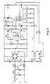
- FIG.3 Another variant is shown in Fig.3. There is no one here Choke more in the connecting line VL and thus in a circle to the electrode E1, but there is a choke DR5 in the circle of the electrode E2, namely in the positive current path of the rectifier D1, D2, D3, D4. With Another throttle DR6 together forms the throttle DR5 of the direct current for the high frequency generator.
- the electrode E2 is on Connection point of the two chokes DR5, DR6 connected.
- the mode of action is basically the same as previously described, except that here the diodes in the rectifier are charged on the DC side.
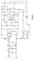
- Fig. 4 also shows a variant.
- This choke DR4 is in the AC supply line between the connection of a second electrode E2 of the gas discharge lamp FL at a power connection P, 0 and the rectifier arrangement D1-D4 and between the terminals of the compensation capacitor C3 and the coupling capacitor C4. This makes it practical same ratio the ratio of active power to apparent power 0.95 increased and the harmonics influencing the AC network are reduced below 10%. In laboratory trials, a performance factor of 99.5 and higher can be measured.
- FIG. 5 basically shows a circuit arrangement has the same structure as the arrangements described above, only that here instead of full-wave rectification with four diodes one Voltage doubler circuit Connected to diodes D10 and D11 is shown with the capacitors C2 and C3.
- the smoothing of the direct current is done with two electrolytic capacitors C4 and C5 each above the DC output from diodes D10 and D11 and phase line P the AC power supply are switched.
- the electrode E2 is natural AC side connected.
- the mode of action is the same as for the aforementioned arrangements by the high frequency voltage only here up to the current amplitude of the alternating voltage can go so that no or very little distortion due to harmonic Vibrations is possible.
Landscapes
- Circuit Arrangements For Discharge Lamps (AREA)
Description
- Fig.1
- ein vollständiges Schaltungsschema einer Anordnung zum Betrieb einer Stromsparlampe mit der Rückführung von der Lampe auf die Netzseite des Gleichrichters,
- Fig.2
- dieselbe Schaltungsanordnung wie in Fig.1 mit einer Variante des Serieschwingkreises für den Betrieb verschieden starker Entladungslampen mit demselben Vorschaltgerät,
- Fig.3
- dieselbe Schaltungsanordnung wie in Fig.1, jedoch mit der Entladungslampe innerhalb des Serieschwingkreises und ihrem Anschluss mit der zweiten Elektrode auf der Gleichstromseite,
- Fig.4
- dieselbe Schaltungsanordnung wie in Fig.1, jedoch mit der zweiten Elektrode wechselstromseitig angeschlossen und einer Anordnung zur Definition der Anstiegsflanke des Gleichrichters, und
- Fig.5
- eine Schaltungsanordnung ähnlich derjenigen gemäss Fig.1, jedoch für eine Speisespannung von 110 V.
Claims (7)
- Schaltungsanordnung zur Ansteuerung von Gasentladungslampen (FL), mit einem Vorschaltgerät zwischen positivem und negativem Pol einer Gleichrichteranordnung (D1-D4), die am Wechselstromnetz mit Phasenleiter (P) und Nulleiter (0) angeschlossen ist,dadurch gekennzeichnet,welches Vorschaltgerät einen Hochfrequenzschwingkreis (R1-R5,T1, T2,C6,I1,I2) umfasst, der einen Glättungskondensator (C5) zum Laden der Gasentladungslampen (FL) schaltet,und bei dem ein Serieschwingkreis (DR3,I3,C8) in der Verbindungsleitung (VL) zwischen einem Ausgang (H) des Hochfrequenzschwingkreises (R1-R5,T1,T2,C6,I1,I2) und dem Eingang der Gleichrichteranordnung (D1-D4) vorhanden ist,dass in der Wechselstromzuleitung von einem Wechselstromanschluss (0,P) zur Gleichrichteranordnung (D1-D4) und zu einem Koppelkondensator (C4) eine zusätzliche Drossel (DR4) geschaltet ist,dass diese Drossel (DR4) über den Koppelkondensator (C4) mit dem Hochfrequenzschwingkreis (R1-R5,T1,T2,C6,I1,I2) und über einen Kompensationskondensator (C3) mit einer zweiten Elektrode (E2) der Gasentladungslampe (FL) verbunden ist,sodass diese Drossel (DR4) mittels einen über die Verbindungsleitung (VL) rückgekoppelten Schwingstrom, der über die Elektrode (E2) und den Kompensationskondensator (C3) fliesst, zum Schwingen angeregt wird und über diese Drossel (DR4) ein Ladepfad (D1-D4;DR4,C4) gebildet wird.
- Schaltungsanordnung zur Ansteuerung von Gasentladungslampen (FL), mit einem Vorschaltgerät zwischen positivem und negativem Pol einer Gleichrichteranordnung (D1-D4), die am Wechselstromnetz mit Phasenleiter (P) und Nulleiter (0) angeschlossen ist,gekennzeichnet durch einen Ladepfad,welches Vorschaltgerät einen Hochfrequenzschwingkreis (R1-R5,T1, T2,C6,I1,I2) umfasst, der einen Glättungskondensator (C5) zum Laden der Gasentladungslampen (FL) schaltet,und bei dem ein Serieschwingkreis (I3,C8) in der Verbindungsleitung (VL) zwischen einem Ausgang (H) des Hochfrequenzschwingkreises (R1-R5,T1,T2,C6,I1,I2) und dem Eingang der Gleichrichteranordnung (D1-D4) vorhanden ist,mit zwei in Reihe geschalteten Drosseln (DR5,DR6), welche Reihenschaltung über einen Verbindungspunkt zwischen den Drosseln (DR5,DR6) am Anschluss einer zweiten Elektrode (E2) der Gasentladungslampe (FL) angeschlossen ist,diese Drosselreihenschaltung (DR5,DR6) ist mit dem Ausgang der Gleichrichteranordnung (D1-D4) verbunden,diese Drosselreihenschaltung (DR5,DR6) ist mit einem Ausgang (H) des Hochfrequenzschwingkreises (R1-R5,T1,T2,C6,I1,I2) verbunden,diese Drosselreihenschaltung (DR5,DR6) ist mit dem Glättungskondensator (C5) verbunden,sodass die Drosseln (DR5,DR6) von der hochfrequenten gleichstromseite aus die Dioden (D1-D4) vom Gleichreichter aufladen.
- Schaltungsanordnung nach Anspruch 1, gekennzeichnet durch einen Ladepfad mit zwei in Reihe geschalteten Dioden (D5,D6), welche Reihenschaltung über einen Verbindungspunkt zwischen den Dioden (D5,D6) mit dem Ausgang (H) des Hochfrequenzschwingkreises (R1-R5,T1,T2,C6,I1,I2) verbunden ist, jede der Dioden (D5,D6) ist antiparallel zu den Emitter-Kollektorstrecken von zwei Transistoren (T1,T2) des Hochfrequenzschwingkreises (R1-R5,T1,T2,C6,I1,I2) geschaltet, diese Diodenreihenschaltung (D5,D6) ist über den Ausgang (H) und den Serieschwingkreis (DR3,I3,C8) mit dem Eingang der Gleichrichteranordnung (D1-D4) verbunden, diese Diodenreihenschaltung (D5,D6) ist parallel zum Glättungskondensator (C5) geschaltet, sodass die Dioden (D5,D6) den Glättungskondensator (C5) mit einer Addition von Hochfrequenzspannung und Netzspannung aufladen und eine Gleichrichtung der mit einer Hochfrequenz überlagerten Niederfrequenz des Wechselstromnetzes durchführen.
- Schaltungsanordnung nach einem der Ansprüche 1 oder 3, dadurch gekennzeichnet, dass eine Elektrode (E1) der Gasentladungslampe (FL) über eine Kapazität (C8) und eine Induktivität (I3,DR3) des Serieschwingkreises (DR3,I3,C8) mit dem Ausgang (H) vom Hochfrequenzschwingkreis (R1-R5,T1,T2,C6,I1,I2) verbunden, wodurch die Gasentladungslampe (FL) über die Verbindungsleitung (VL) in den Serieschwingkreis (DR3,I3,C8) geschaltet wird.
- Schaltungsanordnung nach einem der Ansprüche 1, 3 oder 4, dadurch gekennzeichnet, dass der Serieschwingkreis (DR3,I3,C8) über eine Verbindungsleitung (VL) direkt an einen der Stromanschlüsse (P,0) angeschlossen ist und dass eine zweite Elektrode (E2) der Gasentladungslampe (FL) direkt an einem Stromanschluss (P,0) angeschlossen ist.
- Schaltungsanordnung nach Anspruch 4, dadurch gekennzeichnet, dass die Induktivität (I3) und die Kapazität (C8) des Serieschwingkreises (DR3,I3,C8) als parallele Äste (I3a,I3b,I3c,I3d,C8a,C8b,C8c,C8d) ausgebildet sind und dass der Anschluss zur ersten Elektrode (E1) der Gasentladungslampe (FL) wahlweise an einen der Äste zur Anpassung an die Lichtleistung der Gasentladungslampe (FL) erfolgt.
- Schaltungsanordnung nach einem der Ansprüche 1 bis 6, gekennzeichnet durch eine Vorheizschaltung, bei der zwei Dioden (D8,D9) parallel zu den Dioden (D5,D6) im Hochfrequenzschwingkreis geschaltet sind, deren Mittelabgriff über einen temperaturabhängigen Widerstand (PCT) mit dem Verbindungspunkt zwischen zwei die beiden Elektroden (E1,E2) der Gasentladungslampe (FL) überbrückende Kondensatoren (C12,C13) verbunden ist.
Applications Claiming Priority (3)
| Application Number | Priority Date | Filing Date | Title |
|---|---|---|---|
| CH254694 | 1994-08-18 | ||
| CH254694 | 1994-08-18 | ||
| CH2546/94 | 1994-08-18 |
Publications (3)
| Publication Number | Publication Date |
|---|---|
| EP0697803A2 EP0697803A2 (de) | 1996-02-21 |
| EP0697803A3 EP0697803A3 (de) | 1996-05-01 |
| EP0697803B1 true EP0697803B1 (de) | 2000-03-01 |
Family
ID=4236232
Family Applications (1)
| Application Number | Title | Priority Date | Filing Date |
|---|---|---|---|
| EP95112985A Expired - Lifetime EP0697803B1 (de) | 1994-08-18 | 1995-08-17 | Schaltungsanordnung zur Ansteuerung von Gasentladungslampen |
Country Status (7)
| Country | Link |
|---|---|
| EP (1) | EP0697803B1 (de) |
| JP (1) | JPH0896979A (de) |
| KR (1) | KR100396386B1 (de) |
| CN (1) | CN1118980A (de) |
| AT (1) | ATE190185T1 (de) |
| DE (1) | DE59507872D1 (de) |
| ES (1) | ES2146685T3 (de) |
Families Citing this family (8)
| Publication number | Priority date | Publication date | Assignee | Title |
|---|---|---|---|---|
| DE69625349T2 (de) * | 1996-08-13 | 2003-09-18 | Magnetek Spa | Wechselrichter zum Speisen von Entladungslampen mit Vorrichtung zur Verbesserung des Leistungsfaktors |
| EP0889675A1 (de) * | 1997-07-02 | 1999-01-07 | MAGNETEK S.p.A. | Elektronisches Vorhaltgerät mit Lampentyperkennung |
| US5939837A (en) * | 1997-07-15 | 1999-08-17 | Magnetek, Inc. | Electronic ballast circuit for independently increasing the power factor and decreasing the crest factor |
| KR19990040189U (ko) * | 1998-04-28 | 1999-11-25 | 안치명 | 교류백열등의 페이드아웃 스위치회로 |
| JP2001143886A (ja) * | 1999-11-12 | 2001-05-25 | Asahi National Lighting Co Ltd | 放電灯点灯装置 |
| US6169374B1 (en) * | 1999-12-06 | 2001-01-02 | Philips Electronics North America Corporation | Electronic ballasts with current and voltage feedback paths |
| US6337800B1 (en) | 2000-02-29 | 2002-01-08 | Philips Electronics North American Corporation | Electronic ballast with inductive power feedback |
| US7923941B2 (en) * | 2008-10-16 | 2011-04-12 | General Electric Company | Low cost compact size single stage high power factor circuit for discharge lamps |
Family Cites Families (6)
| Publication number | Priority date | Publication date | Assignee | Title |
|---|---|---|---|---|
| DE3222534A1 (de) | 1982-06-16 | 1983-12-22 | Werner Schoenfeld | Vorschaltgeraet |
| DE3611611A1 (de) | 1986-04-07 | 1987-10-08 | Patent Treuhand Ges Fuer Elektrische Gluehlampen Mbh | Schaltungsanordnung zum hochfrequenten betrieb einer niederdruckentladungslampe |
| DE4005850A1 (de) * | 1990-02-23 | 1991-08-29 | Patent Treuhand Ges Fuer Elektrische Gluehlampen Mbh | Schaltungsanordnung zum betrieb einer entladungslampe |
| CA2056010C (en) * | 1990-11-27 | 1997-05-27 | Minoru Maehara | Inverter device for stable, high power-factor input current supply |
| EP0599405B1 (de) * | 1992-11-26 | 1998-02-11 | Koninklijke Philips Electronics N.V. | Vorschaltgerät mit niedrigem Oberwellengehalt für eine Entladungslampe |
| ES2108201T3 (es) * | 1993-01-12 | 1997-12-16 | Philips Electronics Nv | Circuito de balasto. |
-
1994
- 1994-12-16 CN CN94118428A patent/CN1118980A/zh active Pending
-
1995
- 1995-08-17 ES ES95112985T patent/ES2146685T3/es not_active Expired - Lifetime
- 1995-08-17 DE DE59507872T patent/DE59507872D1/de not_active Expired - Fee Related
- 1995-08-17 JP JP7209772A patent/JPH0896979A/ja active Pending
- 1995-08-17 EP EP95112985A patent/EP0697803B1/de not_active Expired - Lifetime
- 1995-08-17 AT AT95112985T patent/ATE190185T1/de not_active IP Right Cessation
- 1995-08-18 KR KR1019950025352A patent/KR100396386B1/ko not_active Expired - Fee Related
Also Published As
| Publication number | Publication date |
|---|---|
| CN1118980A (zh) | 1996-03-20 |
| KR960009805A (ko) | 1996-03-22 |
| EP0697803A3 (de) | 1996-05-01 |
| DE59507872D1 (de) | 2000-04-06 |
| KR100396386B1 (ko) | 2003-12-06 |
| JPH0896979A (ja) | 1996-04-12 |
| EP0697803A2 (de) | 1996-02-21 |
| ES2146685T3 (es) | 2000-08-16 |
| ATE190185T1 (de) | 2000-03-15 |
Similar Documents
| Publication | Publication Date | Title |
|---|---|---|
| DE69902379T2 (de) | Vorschaltgerät mit helligkeitssteuerung und regelverfahren für lampen unter verwendung eines frequenzgeregelten streufeldtransformators | |
| DE3879548T2 (de) | Wechselrichter zum Zünden und Speisen einer Gasentladungslampe. | |
| EP0253224A2 (de) | Schaltungsanordnung zum Betrieb von Niederdruckentladungslampen | |
| EP0372303B1 (de) | Schaltungsanordnung zum Betrieb einer Niederdruckentladungslampe | |
| EP0679046A1 (de) | Schaltungsanordnung zum Betrieb von Niederdruckentladungslampen | |
| WO1993012631A1 (de) | Schaltungsanordnung zum betrieb einer oder mehrerer niederdruckentladungslampen | |
| DE69315761T2 (de) | Geschützter Umrichter zur Steuerung einer Entladungslampe | |
| DE3829388A1 (de) | Schaltungsanordnung zum betrieb einer last | |
| DE10315473A1 (de) | Schnittstellenschaltung zum Betrieb von kapazitiven Lasten | |
| EP0439240A2 (de) | Elektronisches Vorschaltgerät | |
| EP0541909B1 (de) | Schaltungsanordnung zum Betrieb von Entladungslampen | |
| DE69825718T2 (de) | Glühlampe und Adapter, ausgerüstet mit einer Vorrichtung zur Spannungsumwandlung | |
| JPS5861597A (ja) | 放電灯用電子式安定器 | |
| EP0697803A2 (de) | Schaltungsanordnung zur Ansteuerung von Gasentladungslampen | |
| EP0691800A2 (de) | Schaltungsanordnung zum Betrieb von Niederdruckentladungslampen | |
| EP1028606B1 (de) | Schaltungsanordnung zum Betrieb mindestens einer Niederdruckentladungslampe | |
| EP0155729B1 (de) | Schaltungsanordnung zum Wechselstrombetrieb von Hochdruckgasentladungslampen | |
| DE69714163T2 (de) | Schaltungsanordnung | |
| DE69313256T2 (de) | Ballastschaltung | |
| EP0585727B1 (de) | Wechselrichterschaltung mit zwei in Reihe geschalteten Glättungskapazitäten | |
| DE69313257T2 (de) | Schaltung | |
| DE3429773C2 (de) | ||
| EP0710053B1 (de) | Ansteuerschaltung für eine Stromsparlampe | |
| EP0797377B1 (de) | Verbesserte Halbbrückenansteuerung von Leuchtstofflampen | |
| DD208503A3 (de) | Elektronisches vorschaltgeraet fuer entladungslampen |
Legal Events
| Date | Code | Title | Description |
|---|---|---|---|
| PUAI | Public reference made under article 153(3) epc to a published international application that has entered the european phase |
Free format text: ORIGINAL CODE: 0009012 |
|
| AK | Designated contracting states |
Kind code of ref document: A2 Designated state(s): AT BE CH DE DK ES FR GB GR IE IT LI LU MC NL PT SE |
|
| PUAL | Search report despatched |
Free format text: ORIGINAL CODE: 0009013 |
|
| AK | Designated contracting states |
Kind code of ref document: A3 Designated state(s): AT BE CH DE DK ES FR GB GR IE IT LI LU MC NL PT SE |
|
| 17P | Request for examination filed |
Effective date: 19970117 |
|
| 17Q | First examination report despatched |
Effective date: 19970321 |
|
| GRAG | Despatch of communication of intention to grant |
Free format text: ORIGINAL CODE: EPIDOS AGRA |
|
| GRAG | Despatch of communication of intention to grant |
Free format text: ORIGINAL CODE: EPIDOS AGRA |
|
| GRAH | Despatch of communication of intention to grant a patent |
Free format text: ORIGINAL CODE: EPIDOS IGRA |
|
| GRAH | Despatch of communication of intention to grant a patent |
Free format text: ORIGINAL CODE: EPIDOS IGRA |
|
| GRAA | (expected) grant |
Free format text: ORIGINAL CODE: 0009210 |
|
| RIC1 | Information provided on ipc code assigned before grant |
Free format text: 7H 05B 41/00 A |
|
| AK | Designated contracting states |
Kind code of ref document: B1 Designated state(s): AT BE CH DE DK ES FR GB GR IE IT LI LU MC NL PT SE |
|
| PG25 | Lapsed in a contracting state [announced via postgrant information from national office to epo] |
Ref country code: GR Free format text: LAPSE BECAUSE OF NON-PAYMENT OF DUE FEES Effective date: 20000301 |
|
| REF | Corresponds to: |
Ref document number: 190185 Country of ref document: AT Date of ref document: 20000315 Kind code of ref document: T |
|
| REG | Reference to a national code |
Ref country code: CH Ref legal event code: EP |
|
| GBT | Gb: translation of ep patent filed (gb section 77(6)(a)/1977) |
Effective date: 20000301 |
|
| REF | Corresponds to: |
Ref document number: 59507872 Country of ref document: DE Date of ref document: 20000406 |
|
| REG | Reference to a national code |
Ref country code: IE Ref legal event code: FG4D Free format text: GERMAN |
|
| ITF | It: translation for a ep patent filed | ||
| PG25 | Lapsed in a contracting state [announced via postgrant information from national office to epo] |
Ref country code: PT Free format text: LAPSE BECAUSE OF FAILURE TO SUBMIT A TRANSLATION OF THE DESCRIPTION OR TO PAY THE FEE WITHIN THE PRESCRIBED TIME-LIMIT Effective date: 20000601 Ref country code: DK Free format text: LAPSE BECAUSE OF FAILURE TO SUBMIT A TRANSLATION OF THE DESCRIPTION OR TO PAY THE FEE WITHIN THE PRESCRIBED TIME-LIMIT Effective date: 20000601 |
|
| ET | Fr: translation filed | ||
| RAP2 | Party data changed (patent owner data changed or rights of a patent transferred) |
Owner name: PINBEAM AG |
|
| RIN2 | Information on inventor provided after grant (corrected) |
Free format text: MUESSLI, DANIEL |
|
| REG | Reference to a national code |
Ref country code: ES Ref legal event code: FG2A Ref document number: 2146685 Country of ref document: ES Kind code of ref document: T3 |
|
| PG25 | Lapsed in a contracting state [announced via postgrant information from national office to epo] |
Ref country code: LU Free format text: LAPSE BECAUSE OF NON-PAYMENT OF DUE FEES Effective date: 20000817 |
|
| PG25 | Lapsed in a contracting state [announced via postgrant information from national office to epo] |
Ref country code: MC Free format text: THE PATENT HAS BEEN ANNULLED BY A DECISION OF A NATIONAL AUTHORITY Effective date: 20000831 Ref country code: LI Free format text: LAPSE BECAUSE OF NON-PAYMENT OF DUE FEES Effective date: 20000831 Ref country code: CH Free format text: LAPSE BECAUSE OF NON-PAYMENT OF DUE FEES Effective date: 20000831 Ref country code: BE Free format text: LAPSE BECAUSE OF NON-PAYMENT OF DUE FEES Effective date: 20000831 |
|
| NLS | Nl: assignments of ep-patents |
Owner name: PINBEAM AG |
|
| NLT2 | Nl: modifications (of names), taken from the european patent patent bulletin |
Owner name: PINBEAM AG |
|
| REG | Reference to a national code |
Ref country code: FR Ref legal event code: TP |
|
| PLBE | No opposition filed within time limit |
Free format text: ORIGINAL CODE: 0009261 |
|
| STAA | Information on the status of an ep patent application or granted ep patent |
Free format text: STATUS: NO OPPOSITION FILED WITHIN TIME LIMIT |
|
| PG25 | Lapsed in a contracting state [announced via postgrant information from national office to epo] |
Ref country code: IE Free format text: LAPSE BECAUSE OF NON-PAYMENT OF DUE FEES Effective date: 20010109 |
|
| 26N | No opposition filed | ||
| BERE | Be: lapsed |
Owner name: MUESSLI DANIEL Effective date: 20000831 |
|
| REG | Reference to a national code |
Ref country code: CH Ref legal event code: PL |
|
| REG | Reference to a national code |
Ref country code: CH Ref legal event code: AUV Free format text: DAS OBGENANNTE PATENT IST, MANGELS BEZAHLUNG DER 06. JAHRESGEBUEHR INNERT DER GESETZLICHEN FRIST, DURCH VERFUEGUNG VOM 31.03.2001 ERLOSCHEN. |
|
| REG | Reference to a national code |
Ref country code: GB Ref legal event code: 732E |
|
| REG | Reference to a national code |
Ref country code: GB Ref legal event code: IF02 |
|
| PG25 | Lapsed in a contracting state [announced via postgrant information from national office to epo] |
Ref country code: NL Free format text: LAPSE BECAUSE OF NON-PAYMENT OF DUE FEES Effective date: 20020301 |
|
| NLV4 | Nl: lapsed or anulled due to non-payment of the annual fee |
Effective date: 20020301 |
|
| NLXE | Nl: other communications concerning ep-patents (part 3 heading xe) |
Free format text: A REQUEST FOR RESTORATION TO THE PRIOR STATE (ART. 23 OF THE PATENTS ACT) HAS BEEN FILED ON 20.03.2002. |
|
| NLXE | Nl: other communications concerning ep-patents (part 3 heading xe) |
Free format text: A REQUEST FOR RESTORATION TO THE PRIOR STATE AS PROVIDED FOR IN ARTICLE 23 OF THE PATENTS ACT 1995 (SEE PUBLICATION IN HEADING XE OF THE PATENT BULLETIN OF 20020603/06) HAS BEEN GRANTED; THE RESTORATION OF THE PATENT HAS BEEN ENTERED IN THE PATENT REGISTER. |
|
| PGFP | Annual fee paid to national office [announced via postgrant information from national office to epo] |
Ref country code: NL Payment date: 20060824 Year of fee payment: 12 Ref country code: GB Payment date: 20060824 Year of fee payment: 12 Ref country code: FR Payment date: 20060824 Year of fee payment: 12 Ref country code: DE Payment date: 20060824 Year of fee payment: 12 |
|
| PGFP | Annual fee paid to national office [announced via postgrant information from national office to epo] |
Ref country code: AT Payment date: 20060825 Year of fee payment: 12 |
|
| PGFP | Annual fee paid to national office [announced via postgrant information from national office to epo] |
Ref country code: ES Payment date: 20060830 Year of fee payment: 12 |
|
| PGFP | Annual fee paid to national office [announced via postgrant information from national office to epo] |
Ref country code: IT Payment date: 20060831 Year of fee payment: 12 |
|
| PGFP | Annual fee paid to national office [announced via postgrant information from national office to epo] |
Ref country code: SE Payment date: 20060824 Year of fee payment: 12 |
|
| EUG | Se: european patent has lapsed | ||
| GBPC | Gb: european patent ceased through non-payment of renewal fee |
Effective date: 20070817 |
|
| PG25 | Lapsed in a contracting state [announced via postgrant information from national office to epo] |
Ref country code: SE Free format text: LAPSE BECAUSE OF NON-PAYMENT OF DUE FEES Effective date: 20070818 |
|
| NLV4 | Nl: lapsed or anulled due to non-payment of the annual fee |
Effective date: 20080301 |
|
| PG25 | Lapsed in a contracting state [announced via postgrant information from national office to epo] |
Ref country code: AT Free format text: LAPSE BECAUSE OF NON-PAYMENT OF DUE FEES Effective date: 20070817 |
|
| REG | Reference to a national code |
Ref country code: FR Ref legal event code: ST Effective date: 20080430 |
|
| PG25 | Lapsed in a contracting state [announced via postgrant information from national office to epo] |
Ref country code: DE Free format text: LAPSE BECAUSE OF NON-PAYMENT OF DUE FEES Effective date: 20080301 |
|
| PG25 | Lapsed in a contracting state [announced via postgrant information from national office to epo] |
Ref country code: FR Free format text: LAPSE BECAUSE OF NON-PAYMENT OF DUE FEES Effective date: 20070831 |
|
| REG | Reference to a national code |
Ref country code: ES Ref legal event code: FD2A Effective date: 20070818 |
|
| PG25 | Lapsed in a contracting state [announced via postgrant information from national office to epo] |
Ref country code: GB Free format text: LAPSE BECAUSE OF NON-PAYMENT OF DUE FEES Effective date: 20070817 |
|
| PG25 | Lapsed in a contracting state [announced via postgrant information from national office to epo] |
Ref country code: ES Free format text: LAPSE BECAUSE OF NON-PAYMENT OF DUE FEES Effective date: 20070818 |
|
| PG25 | Lapsed in a contracting state [announced via postgrant information from national office to epo] |
Ref country code: IT Free format text: LAPSE BECAUSE OF NON-PAYMENT OF DUE FEES Effective date: 20070817 |