EP0694936A1 - Trapezoid- or arc-shaped chip component - Google Patents
Trapezoid- or arc-shaped chip component Download PDFInfo
- Publication number
- EP0694936A1 EP0694936A1 EP95110498A EP95110498A EP0694936A1 EP 0694936 A1 EP0694936 A1 EP 0694936A1 EP 95110498 A EP95110498 A EP 95110498A EP 95110498 A EP95110498 A EP 95110498A EP 0694936 A1 EP0694936 A1 EP 0694936A1
- Authority
- EP
- European Patent Office
- Prior art keywords
- electronic element
- electronic
- shape
- plate electrode
- elements
- Prior art date
- Legal status (The legal status is an assumption and is not a legal conclusion. Google has not performed a legal analysis and makes no representation as to the accuracy of the status listed.)
- Granted
Links
Images


Classifications
-
- H—ELECTRICITY
- H01—ELECTRIC ELEMENTS
- H01G—CAPACITORS; CAPACITORS, RECTIFIERS, DETECTORS, SWITCHING DEVICES OR LIGHT-SENSITIVE DEVICES, OF THE ELECTROLYTIC TYPE
- H01G9/00—Electrolytic capacitors, rectifiers, detectors, switching devices, light-sensitive or temperature-sensitive devices; Processes of their manufacture
- H01G9/004—Details
- H01G9/008—Terminals
- H01G9/012—Terminals specially adapted for solid capacitors
-
- H—ELECTRICITY
- H01—ELECTRIC ELEMENTS
- H01G—CAPACITORS; CAPACITORS, RECTIFIERS, DETECTORS, SWITCHING DEVICES OR LIGHT-SENSITIVE DEVICES, OF THE ELECTROLYTIC TYPE
- H01G9/00—Electrolytic capacitors, rectifiers, detectors, switching devices, light-sensitive or temperature-sensitive devices; Processes of their manufacture
- H01G9/15—Solid electrolytic capacitors
Definitions
- the present invention relates to an outside-insulated electronic element of a cubic chip type, and more particularly to an outside-insulated electronic element which can be stably stored in a disk form package having a spiral groove.
- FIG. 1 A conventional cubical electronic element 1 of a chip type is shown in Fig. 1, in which a plate type electrode terminal 2 extending from a body 3 of the electronic element is bent along a side surface and a bottom surface of the body 3 of the electronic element, and in which the body 3 of the electronic element including the plate type electrode terminal 2 is of a parallelpiped solid (as disclosed, for example, in Japanese Utility Model Application Kokoku Publication No. Hei 1-32737).
- An object of the present invention is to overcome the problems existing in the prior art and to provide an outside-insulated electronic element which can be stably stored in a disk package having a spiral groove.
- an outside-insulated electronic element of a chip type comprising: a body of the electronic element which has a trapezoidal or arcuate shape; and a plate electrode which extends from the body of the element and is bent along a side surface and a bottom surface of the body of the element.
- the electronic element is configured in a trapezoidal shape or a bow or arcuate shape, or the electronic element including the plate electrode terminal is configured in such a shape, the gaps amongst the electronic elements when placed in a disk package can be reduced to a minimum. In this way, the electronic elements are stably stored in the disk package, whereby the electronic element reliability can be ensured and the occurrence of static electricity can be suppressed.
- Fig. 3 shows a groove spirally formed in a disk package 7.
- a radius of curvature of the spiral groove is represented by R.
- Fig. 4 shows, in a perspective view, an electronic element 8 of a first embodiment according to the invention.
- a capacitor element is fabricated by forming a negative pole layer on a positive pole body of a tantalum valve action metal powder with an oxide layer, a semiconductor layer, and a graphite layer sequentially interposed therebetween.
- This capacitor element is electrically connected to a plate type electrode terminal 2 using an electrical welding process or a conductive adhesive agent.
- the electronic element 8 including a part of the plate type electrode terminal 2 is resin-molded using, for example, epoxy resin and employing, for example, a transfer mold process using a trapezoidal metal mold. Thereafter, the part of the electrode terminal 2 that is exposed from the body of the trapezoidal electronic element 8 is bent along the body thereof, and this completes the chip tantalum capacitor.
- the radius of curvature thereof becomes 5 cm which corresponds to that of the outermost disk groove.
- Fig. 5 shows, when the electronic elements 8 are placed continuously in the spiral groove 5 in the disk package, the reduced gap between one electronic element and the adjacent electronic element, which is in contrast to that in the prior art shown in Fig. 2.
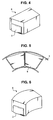
- Fig. 6 shows, in a perspective view, an electronic element 9 of a second embodiment according to the invention.
- the electronic element 9 is resin-molded using the same transfer mold process as used for the first embodiment explained above.
- the electronic element 9 is molded by the metal mold such that the element is shaped into a bow or arcuate form and that a plurality of elements, when placed adjacent to each other, form a radius of curvature of between 1 and 5 cm.
- the electronic element 9 has a trapezoidal shape combined with a bow shape formed by arcuate front and back surfaces.
- Fig. 7 shows, in a perspective view, an electronic element 10 of a third embodiment according to the invention.
- the plate electrode terminal 11 extending from the body of the element is inclined and is non-parallel with respect to the side surface thereof. That is, the combination of the body of the electronic element and the plate electrode becomes trapezoidal in shape.
- the electronic element 10 and the plate electrode terminal 11 thus configured attain the same advantages as those attained in the first and second embodiments explained above.
- Fig. 8 shows, in a perspective view, an electronic element 12 of a fourth embodiment according to the invention.
- the body of the electronic element 12 is shaped such that the front and back surfaces of the body thereof are of a trapezoidal shape.
- the element 12 thus formed is placed in a disk package with the front facing upward.
Landscapes
- Engineering & Computer Science (AREA)
- Power Engineering (AREA)
- Microelectronics & Electronic Packaging (AREA)
- Packaging Frangible Articles (AREA)
- Fixed Capacitors And Capacitor Manufacturing Machines (AREA)
- Packaging For Recording Disks (AREA)
Abstract
Description
- The present invention relates to an outside-insulated electronic element of a cubic chip type, and more particularly to an outside-insulated electronic element which can be stably stored in a disk form package having a spiral groove.
- A conventional cubical electronic element 1 of a chip type is shown in Fig. 1, in which a plate
type electrode terminal 2 extending from abody 3 of the electronic element is bent along a side surface and a bottom surface of thebody 3 of the electronic element, and in which thebody 3 of the electronic element including the platetype electrode terminal 2 is of a parallelpiped solid (as disclosed, for example, in Japanese Utility Model Application Kokoku Publication No. Hei 1-32737). - Electronic elements of a chip type are placed in a groove spirally formed as shown in Fig. 3 in a
disk package 7. When conventional cubical electronic elements 1 of chip types are placed continuously in thespiral groove 5 in the disk package, since each of such elements is shaped as parallelpiped solid, there remains alarge gap 6 as shown in Fig. 2 between one element and an adjacent element. Thisgap 6 is undesirable as the elements are allowed to move or vibrate due to this gap, thereby leading to the lowering of element reliability and the occurrence of static electricity. Also, during the course of continuous insertion of the parallelpiped solid elements 1 into the disk package, the flow of the elements tends to be hindered and the elements being inserted become stuck in the spiral groove of the disk package, thereby affecting the storing efficiency of the disk packages. A further problem is that, where the shape of the element is of a cubic solid with its right and left sides being symmetrical, there is a possibility for the element to be inserted back-to-front, which is a problem in the case of an element having polarity. - An object of the present invention, therefore, is to overcome the problems existing in the prior art and to provide an outside-insulated electronic element which can be stably stored in a disk package having a spiral groove.
- According to one aspect of the invention, there is provided an outside-insulated electronic element of a chip type comprising:
a body of the electronic element which has a trapezoidal or arcuate shape; and
a plate electrode which extends from the body of the element and is bent along a side surface and a bottom surface of the body of the element. - According to the invention, since the electronic element is configured in a trapezoidal shape or a bow or arcuate shape, or the electronic element including the plate electrode terminal is configured in such a shape, the gaps amongst the electronic elements when placed in a disk package can be reduced to a minimum. In this way, the electronic elements are stably stored in the disk package, whereby the electronic element reliability can be ensured and the occurrence of static electricity can be suppressed.
- The above and other objects, features and advantages of the present invention will be apparent from the following description of preferred embodiments of the invention explained with reference to the accompanying drawings, in which:
- Fig. 1 is a perspective view of a conventional electronic element of a cubical chip type;
- Fig. 2 is a top view of a spiral groove in a part of a disk package in which conventional electronic elements of cubical chip types are inserted;
- Fig. 3 is a perspective view of a disk package, showing a groove spirally formed in a disk package;
- Fig. 4 is a perspective view of an electronic element of a first embodiment according to the invention;
- Fig. 5 is a top view of a spiral groove of a part of a disk package in which the electronic elements of the first embodiment according to the invention are inserted;
- Fig. 6 is a perspective view of an electronic element of a second embodiment according to the invention;
- Fig. 7 is a perspective view of an electronic element of a third embodiment according to the invention; and
- Fig. 8 is a perspective view of an electronic element of a fourth embodiment according to the invention.
- Now, preferred embodiments of the invention are explained with reference to the drawings.
- Fig. 3 shows a groove spirally formed in a
disk package 7. A radius of curvature of the spiral groove is represented by R. - Fig. 4 shows, in a perspective view, an
electronic element 8 of a first embodiment according to the invention. - The explanation is given here with reference to a tantalum capacitor as an example.
- In the manufacture of the chip tantalum capacitor, a capacitor element is fabricated by forming a negative pole layer on a positive pole body of a tantalum valve action metal powder with an oxide layer, a semiconductor layer, and a graphite layer sequentially interposed therebetween. This capacitor element is electrically connected to a plate
type electrode terminal 2 using an electrical welding process or a conductive adhesive agent. - Then, the
electronic element 8 including a part of the platetype electrode terminal 2 is resin-molded using, for example, epoxy resin and employing, for example, a transfer mold process using a trapezoidal metal mold. Thereafter, the part of theelectrode terminal 2 that is exposed from the body of the trapezoidalelectronic element 8 is bent along the body thereof, and this completes the chip tantalum capacitor. - When the chip tantalum capacitors, that is, cubic chip type electronic elements, are continuously placed one after another, the radius of curvature thereof becomes 5 cm which corresponds to that of the outermost disk groove.
- Fig. 5 shows, when the
electronic elements 8 are placed continuously in thespiral groove 5 in the disk package, the reduced gap between one electronic element and the adjacent electronic element, which is in contrast to that in the prior art shown in Fig. 2. - Fig. 6 shows, in a perspective view, an
electronic element 9 of a second embodiment according to the invention. - The
electronic element 9 is resin-molded using the same transfer mold process as used for the first embodiment explained above. In this case, theelectronic element 9 is molded by the metal mold such that the element is shaped into a bow or arcuate form and that a plurality of elements, when placed adjacent to each other, form a radius of curvature of between 1 and 5 cm. Theelectronic element 9 has a trapezoidal shape combined with a bow shape formed by arcuate front and back surfaces. - Fig. 7 shows, in a perspective view, an
electronic element 10 of a third embodiment according to the invention. - In this embodiment, while the
electronic element 10 is configured in a parallelpiped solid shape, theplate electrode terminal 11 extending from the body of the element is inclined and is non-parallel with respect to the side surface thereof. That is, the combination of the body of the electronic element and the plate electrode becomes trapezoidal in shape. Theelectronic element 10 and theplate electrode terminal 11 thus configured attain the same advantages as those attained in the first and second embodiments explained above. - Fig. 8 shows, in a perspective view, an
electronic element 12 of a fourth embodiment according to the invention. - In this embedment, the body of the
electronic element 12 is shaped such that the front and back surfaces of the body thereof are of a trapezoidal shape. Theelement 12 thus formed is placed in a disk package with the front facing upward. This embodiment provides the same advantages as those provided by the first to the third embodiment explained above. - While the invention has been described in its preferred embodiments, it is to be understood that the words which have been used are words of description rather than limitation and that changes within the purview of the appended claims may be made without departing from the true scope and spirit of the invention as defined by the claims.
Claims (4)
- An outside-insulated electronic element (8,10,12) of a chip type, characterized by comprising:
a body of the electronic element which has a trapezoidal shape; and
a plate electrode (2,11) which extends from said body of the element and is bent along a side surface and a bottom surface of said body of the element. - The outside-insulated electronic element of a chip type according to claim 1, in which the body of said electronic element (10) including said plate electrode (11) is trapezoidal in shape.
- The outside-insulated electronic element of a chip type according to claim 1, in which the body of said electronic element (12) is shaped into a trapezoidal form by front and back trapezoidal surfaces.
- An outside-insulated electronic element (9) of a chip type, characterized by comprising:
a body of the electronic element which has an arcuate shape; and
a plate electrode (2) which extends from said body of the element and is bent along a side surface and a bottom surface of said body of the element.
Applications Claiming Priority (2)
| Application Number | Priority Date | Filing Date | Title |
|---|---|---|---|
| JP6166863A JPH0831687A (en) | 1994-07-19 | 1994-07-19 | Angular chip-form electronic parts |
| JP166863/94 | 1994-07-19 |
Publications (2)
| Publication Number | Publication Date |
|---|---|
| EP0694936A1 true EP0694936A1 (en) | 1996-01-31 |
| EP0694936B1 EP0694936B1 (en) | 1997-03-19 |
Family
ID=15839043
Family Applications (1)
| Application Number | Title | Priority Date | Filing Date |
|---|---|---|---|
| EP95110498A Expired - Lifetime EP0694936B1 (en) | 1994-07-19 | 1995-07-05 | Trapezoid- or arc-shaped chip component |
Country Status (4)
| Country | Link |
|---|---|
| US (1) | US5566054A (en) |
| EP (1) | EP0694936B1 (en) |
| JP (1) | JPH0831687A (en) |
| DE (1) | DE69500188T2 (en) |
Cited By (1)
| Publication number | Priority date | Publication date | Assignee | Title |
|---|---|---|---|---|
| EP1385089A2 (en) | 2002-07-26 | 2004-01-28 | Ricoh Company, Ltd. | Image forming apparatus, information processing apparatus, program execution method and program producing method |
Families Citing this family (1)
| Publication number | Priority date | Publication date | Assignee | Title |
|---|---|---|---|---|
| JP5975053B2 (en) * | 2014-03-07 | 2016-08-23 | 株式会社村田製作所 | Capacitor module and power conversion system |
Citations (4)
| Publication number | Priority date | Publication date | Assignee | Title |
|---|---|---|---|---|
| FR2146223A1 (en) * | 1971-07-19 | 1973-03-02 | Matsuo Electric Co | |
| JPH0132737Y2 (en) | 1983-02-22 | 1989-10-05 | ||
| JPH04150042A (en) * | 1990-10-12 | 1992-05-22 | Nec Corp | Manufacture of semiconductor device |
| JPH1068915A (en) * | 1996-08-27 | 1998-03-10 | Tokin Corp | Branch interference type optical waveguide and electric field sensor formed by using the same |
Family Cites Families (7)
| Publication number | Priority date | Publication date | Assignee | Title |
|---|---|---|---|---|
| JPS602801B2 (en) * | 1976-12-03 | 1985-01-24 | 日本電気株式会社 | Double reflector shaped beam antenna |
| JPS5786151A (en) * | 1980-11-18 | 1982-05-29 | Pioneer Electronic Corp | Tape recorder |
| JPS60220922A (en) * | 1985-04-01 | 1985-11-05 | 日立エーアイシー株式会社 | Chip type capacitor |
| JPS63239965A (en) * | 1987-03-27 | 1988-10-05 | Oki Electric Ind Co Ltd | Semiconductor device |
| GB2208333B (en) * | 1987-07-24 | 1991-03-13 | Plessey Co Plc | A method of connection and a module for use therein |
| JPS6432737A (en) * | 1987-07-29 | 1989-02-02 | Fujitsu Ltd | Abnormalness detection system |
| US5388024A (en) * | 1993-08-02 | 1995-02-07 | Avx Corporation | Trapezoid chip capacitor |
-
1994
- 1994-07-19 JP JP6166863A patent/JPH0831687A/en active Pending
-
1995
- 1995-07-05 DE DE69500188T patent/DE69500188T2/en not_active Expired - Fee Related
- 1995-07-05 EP EP95110498A patent/EP0694936B1/en not_active Expired - Lifetime
- 1995-07-06 US US08/498,599 patent/US5566054A/en not_active Expired - Fee Related
Patent Citations (4)
| Publication number | Priority date | Publication date | Assignee | Title |
|---|---|---|---|---|
| FR2146223A1 (en) * | 1971-07-19 | 1973-03-02 | Matsuo Electric Co | |
| JPH0132737Y2 (en) | 1983-02-22 | 1989-10-05 | ||
| JPH04150042A (en) * | 1990-10-12 | 1992-05-22 | Nec Corp | Manufacture of semiconductor device |
| JPH1068915A (en) * | 1996-08-27 | 1998-03-10 | Tokin Corp | Branch interference type optical waveguide and electric field sensor formed by using the same |
Non-Patent Citations (2)
| Title |
|---|
| PATENT ABSTRACTS OF JAPAN vol. 13, no. 285 (E - 780) 29 June 1989 (1989-06-29) * |
| PATENT ABSTRACTS OF JAPAN vol. 16, no. 429 (E - 1261) 8 September 1992 (1992-09-08) * |
Cited By (1)
| Publication number | Priority date | Publication date | Assignee | Title |
|---|---|---|---|---|
| EP1385089A2 (en) | 2002-07-26 | 2004-01-28 | Ricoh Company, Ltd. | Image forming apparatus, information processing apparatus, program execution method and program producing method |
Also Published As
| Publication number | Publication date |
|---|---|
| EP0694936B1 (en) | 1997-03-19 |
| US5566054A (en) | 1996-10-15 |
| DE69500188D1 (en) | 1997-04-24 |
| JPH0831687A (en) | 1996-02-02 |
| DE69500188T2 (en) | 1997-10-16 |
Similar Documents
| Publication | Publication Date | Title |
|---|---|---|
| US6522230B2 (en) | Chip-type common mode choke coil | |
| EP0694936B1 (en) | Trapezoid- or arc-shaped chip component | |
| EP3703160B1 (en) | Secondary battery | |
| JP3241102B2 (en) | Noise filter | |
| JPH11191515A (en) | Electronic component with lead | |
| JP2845010B2 (en) | Solid electrolytic capacitors | |
| JP2697018B2 (en) | 4 terminal chip type solid electrolytic capacitor | |
| JP2655629B2 (en) | Chip type solid electrolytic capacitor | |
| JPS6337492B2 (en) | ||
| JPH0547446Y2 (en) | ||
| KR950001584Y1 (en) | Insulating paper for film condenser | |
| JP3441817B2 (en) | Chip electronic components | |
| JP3015266U (en) | Electronic parts | |
| JP2908896B2 (en) | Electrodes for spiral-wound batteries | |
| JPS61236103A (en) | Metal oxide chip varistor | |
| JP2006012955A (en) | Electronic component | |
| JPH05343272A (en) | Solid electrolytic capacitor | |
| JPS63184312A (en) | Chip capacitor | |
| JPS632361A (en) | Electronic device | |
| JP2001023867A (en) | Electronic part | |
| JPS6158227A (en) | Chip type electrolytic condenser | |
| JPS588938U (en) | Chip type electronic components | |
| JPS63160320A (en) | Thin electric component | |
| JPS61202412A (en) | Chip-like electronic component | |
| JPS5827318A (en) | Structure for trimmer condenser |
Legal Events
| Date | Code | Title | Description |
|---|---|---|---|
| PUAI | Public reference made under article 153(3) epc to a published international application that has entered the european phase |
Free format text: ORIGINAL CODE: 0009012 |
|
| 17P | Request for examination filed |
Effective date: 19951018 |
|
| AK | Designated contracting states |
Kind code of ref document: A1 Designated state(s): DE FR GB |
|
| GRAG | Despatch of communication of intention to grant |
Free format text: ORIGINAL CODE: EPIDOS AGRA |
|
| GRAH | Despatch of communication of intention to grant a patent |
Free format text: ORIGINAL CODE: EPIDOS IGRA |
|
| 17Q | First examination report despatched |
Effective date: 19960805 |
|
| GRAH | Despatch of communication of intention to grant a patent |
Free format text: ORIGINAL CODE: EPIDOS IGRA |
|
| GRAA | (expected) grant |
Free format text: ORIGINAL CODE: 0009210 |
|
| AK | Designated contracting states |
Kind code of ref document: B1 Designated state(s): DE FR GB |
|
| REF | Corresponds to: |
Ref document number: 69500188 Country of ref document: DE Date of ref document: 19970424 |
|
| ET | Fr: translation filed | ||
| PLBE | No opposition filed within time limit |
Free format text: ORIGINAL CODE: 0009261 |
|
| STAA | Information on the status of an ep patent application or granted ep patent |
Free format text: STATUS: NO OPPOSITION FILED WITHIN TIME LIMIT |
|
| 26N | No opposition filed | ||
| REG | Reference to a national code |
Ref country code: GB Ref legal event code: IF02 |
|
| PGFP | Annual fee paid to national office [announced via postgrant information from national office to epo] |
Ref country code: GB Payment date: 20020703 Year of fee payment: 8 |
|
| PGFP | Annual fee paid to national office [announced via postgrant information from national office to epo] |
Ref country code: FR Payment date: 20020709 Year of fee payment: 8 |
|
| PGFP | Annual fee paid to national office [announced via postgrant information from national office to epo] |
Ref country code: DE Payment date: 20020710 Year of fee payment: 8 |
|
| REG | Reference to a national code |
Ref country code: GB Ref legal event code: 732E |
|
| REG | Reference to a national code |
Ref country code: FR Ref legal event code: TP |
|
| PG25 | Lapsed in a contracting state [announced via postgrant information from national office to epo] |
Ref country code: GB Free format text: LAPSE BECAUSE OF NON-PAYMENT OF DUE FEES Effective date: 20030705 |
|
| PG25 | Lapsed in a contracting state [announced via postgrant information from national office to epo] |
Ref country code: DE Free format text: LAPSE BECAUSE OF NON-PAYMENT OF DUE FEES Effective date: 20040203 |
|
| GBPC | Gb: european patent ceased through non-payment of renewal fee |
Effective date: 20030705 |
|
| PG25 | Lapsed in a contracting state [announced via postgrant information from national office to epo] |
Ref country code: FR Free format text: LAPSE BECAUSE OF NON-PAYMENT OF DUE FEES Effective date: 20040331 |
|
| REG | Reference to a national code |
Ref country code: FR Ref legal event code: ST |