EP0690501A2 - Integrated circuit package with diamond heat sink - Google Patents
Integrated circuit package with diamond heat sink Download PDFInfo
- Publication number
- EP0690501A2 EP0690501A2 EP95201765A EP95201765A EP0690501A2 EP 0690501 A2 EP0690501 A2 EP 0690501A2 EP 95201765 A EP95201765 A EP 95201765A EP 95201765 A EP95201765 A EP 95201765A EP 0690501 A2 EP0690501 A2 EP 0690501A2
- Authority
- EP
- European Patent Office
- Prior art keywords
- package
- base
- integrated circuit
- diamond
- legs
- Prior art date
- Legal status (The legal status is an assumption and is not a legal conclusion. Google has not performed a legal analysis and makes no representation as to the accuracy of the status listed.)
- Ceased
Links
Images

Classifications
-
- H—ELECTRICITY
- H10—SEMICONDUCTOR DEVICES; ELECTRIC SOLID-STATE DEVICES NOT OTHERWISE PROVIDED FOR
- H10W—GENERIC PACKAGES, INTERCONNECTIONS, CONNECTORS OR OTHER CONSTRUCTIONAL DETAILS OF DEVICES COVERED BY CLASS H10
- H10W40/00—Arrangements for thermal protection or thermal control
-
- H—ELECTRICITY
- H10—SEMICONDUCTOR DEVICES; ELECTRIC SOLID-STATE DEVICES NOT OTHERWISE PROVIDED FOR
- H10W—GENERIC PACKAGES, INTERCONNECTIONS, CONNECTORS OR OTHER CONSTRUCTIONAL DETAILS OF DEVICES COVERED BY CLASS H10
- H10W40/00—Arrangements for thermal protection or thermal control
- H10W40/70—Fillings or auxiliary members in containers or in encapsulations for thermal protection or control
- H10W40/77—Auxiliary members characterised by their shape
- H10W40/778—Auxiliary members characterised by their shape in encapsulations
-
- H—ELECTRICITY
- H10—SEMICONDUCTOR DEVICES; ELECTRIC SOLID-STATE DEVICES NOT OTHERWISE PROVIDED FOR
- H10W—GENERIC PACKAGES, INTERCONNECTIONS, CONNECTORS OR OTHER CONSTRUCTIONAL DETAILS OF DEVICES COVERED BY CLASS H10
- H10W40/00—Arrangements for thermal protection or thermal control
- H10W40/20—Arrangements for cooling
- H10W40/25—Arrangements for cooling characterised by their materials
- H10W40/254—Diamond
-
- H—ELECTRICITY
- H10—SEMICONDUCTOR DEVICES; ELECTRIC SOLID-STATE DEVICES NOT OTHERWISE PROVIDED FOR
- H10W—GENERIC PACKAGES, INTERCONNECTIONS, CONNECTORS OR OTHER CONSTRUCTIONAL DETAILS OF DEVICES COVERED BY CLASS H10
- H10W72/00—Interconnections or connectors in packages
- H10W72/071—Connecting or disconnecting
- H10W72/075—Connecting or disconnecting of bond wires
-
- H—ELECTRICITY
- H10—SEMICONDUCTOR DEVICES; ELECTRIC SOLID-STATE DEVICES NOT OTHERWISE PROVIDED FOR
- H10W—GENERIC PACKAGES, INTERCONNECTIONS, CONNECTORS OR OTHER CONSTRUCTIONAL DETAILS OF DEVICES COVERED BY CLASS H10
- H10W72/00—Interconnections or connectors in packages
- H10W72/50—Bond wires
- H10W72/541—Dispositions of bond wires
- H10W72/5449—Dispositions of bond wires not being orthogonal to a side surface of the chip, e.g. fan-out arrangements
-
- H—ELECTRICITY
- H10—SEMICONDUCTOR DEVICES; ELECTRIC SOLID-STATE DEVICES NOT OTHERWISE PROVIDED FOR
- H10W—GENERIC PACKAGES, INTERCONNECTIONS, CONNECTORS OR OTHER CONSTRUCTIONAL DETAILS OF DEVICES COVERED BY CLASS H10
- H10W72/00—Interconnections or connectors in packages
- H10W72/50—Bond wires
- H10W72/551—Materials of bond wires
- H10W72/552—Materials of bond wires comprising metals or metalloids, e.g. silver
- H10W72/5522—Materials of bond wires comprising metals or metalloids, e.g. silver comprising gold [Au]
-
- H—ELECTRICITY
- H10—SEMICONDUCTOR DEVICES; ELECTRIC SOLID-STATE DEVICES NOT OTHERWISE PROVIDED FOR
- H10W—GENERIC PACKAGES, INTERCONNECTIONS, CONNECTORS OR OTHER CONSTRUCTIONAL DETAILS OF DEVICES COVERED BY CLASS H10
- H10W72/00—Interconnections or connectors in packages
- H10W72/90—Bond pads, in general
- H10W72/951—Materials of bond pads
- H10W72/952—Materials of bond pads comprising metals or metalloids, e.g. PbSn, Ag or Cu
-
- H—ELECTRICITY
- H10—SEMICONDUCTOR DEVICES; ELECTRIC SOLID-STATE DEVICES NOT OTHERWISE PROVIDED FOR
- H10W—GENERIC PACKAGES, INTERCONNECTIONS, CONNECTORS OR OTHER CONSTRUCTIONAL DETAILS OF DEVICES COVERED BY CLASS H10
- H10W74/00—Encapsulations, e.g. protective coatings
-
- H—ELECTRICITY
- H10—SEMICONDUCTOR DEVICES; ELECTRIC SOLID-STATE DEVICES NOT OTHERWISE PROVIDED FOR
- H10W—GENERIC PACKAGES, INTERCONNECTIONS, CONNECTORS OR OTHER CONSTRUCTIONAL DETAILS OF DEVICES COVERED BY CLASS H10
- H10W90/00—Package configurations
- H10W90/701—Package configurations characterised by the relative positions of pads or connectors relative to package parts
- H10W90/751—Package configurations characterised by the relative positions of pads or connectors relative to package parts of bond wires
- H10W90/756—Package configurations characterised by the relative positions of pads or connectors relative to package parts of bond wires between a chip and a stacked lead frame, conducting package substrate or heat sink
Definitions
- an integrated circuit chip 2 having a plurality of chip bonding pads 3 at its perimeter is fastened to a die substrate 4 which is held by two tie bars 5 embedded in thermoplastic molding compound 6, such as a polyamide.
- a plurality of metal legs, or leads 7 are also embedded in the plastic compound 6 with (typically) nickel-plated wire bonding pads 8 at their inner ends.
- the leads 7 and substrate 4 are parts which have been separated from a lead frame in the course of assembly of the package 1.
- Lead wires 9 are bonded to the pads 3 and the bonding pads 8 of the leads 7 to connect the chip 2 to the leads 7, which provide connection means to other circuit components.
- thermal density Because electrical inefficiencies in the chip generate heat, the temperature of both the chip 2 and other parts of the package supporting the chip 2 significantly rise during use. It is known that such elevated temperatures can degrade the system's performance. For example, because many of the system's critical processes rely on kinetic phenomena which become accelerated by increased temperature, failures in metallization and bonded interfaces occur during extended use. Accordingly, heat production by the chip, often termed "thermal density", has become a significant design consideration which threatens to limit the further miniaturization of information systems within reasonable cost constraints.
- thermal conduits are only marginally effective.
- the wires are poor thermal conduits because they have a small cross section (i.e., about 0.002 inch thickness).
- the die pads while having a good cross section (i.e., about 0.010 inch thickness) are ineffective thermal conduits because they are truncated at each end of the IC package, and so there are no metal thermal paths available to the outside after the IC molding process.
- the plastic molding has an extremely low thermal conductivity.
- thermal dissipation connects a more thermally conductive, high surface area material (known as a "heat spreader") to the chip.
- heat spreaders succeed in dissipating hot spots on the chip, they do not significantly assist in removing heat from the package as a whole.
- Another present improvement involves blowing air across either the chip or attached heat spreader, thereby removing heat convectively from the package. Although this improvement succeeds in removing more heat from the package, it adds cost and requires geometry changes in the area around the package.
- a plastic encapsulated integrated circuit package comprising:
- an integrated circuit package comprising:
- FIG 1 is an elevated perspective view of a conventional dual in-line integrated circuit package (DIP).
- DIP dual in-line integrated circuit package
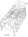
- Figure 2 is an elevated perspective view of the present invention.
- intimate thermal contact means that the thermal conductivity of the interface connecting the device die pad to the lead exceeds 2 W/cm K, so that there is essentially no thermal resistance provided by any gap therebetween.
- the base touches both the leads and the chip.
- any substrate having a thermal conductivity of at least about 2 W/cm K and an electrical resisitivity of at least about 10 E6 ohm-cm at 10 V dc can be used as the thermally conductive, electrically resisitive base of the present invention.
- These substrates include, but are not limited to, diamond, aluminum nitride, beryllia, diamond-coated substrates, and insulator-clad metals.
- the thermal conductivity of the base is at least about 6 W/cm K, more preferably at least about 10 W/cm K.
- the electrical resisitivity of the base is at least about 10E8 ohm-cm, more preferably exceeds 10 E10 ohm-cm.
- the thickness of the base may be between about 100 and about 500 um, preferably between about 150 and 200 um.
- the base is diamond film because it is both an excellent thermal conductor and an excellent electrical insulator.
- Such diamond film can be any high thermal conductivity diamond (free standing or coating).
- the base is a diamond film having a thermal conductivity of at least about 10 W/cm K and an electrical resisitivity of at least about 10 E10 ohm-cm.
- the diamond film is chemically vapor deposited (CVD) diamond which has a thickness of between about 150 and about 200 microns. Because the diamond film can be so thin, its utilization in the present invention offers a design advantage in that it can be incorporated into conventional system designs without a significant change in the package geometry.
- a plastic encapsulated IC package 24 comprising a chip 11 having die pads 12 which is mounted upon a diamond substrate 20.
- Leads or legs 13 having leg connection bonding pads 14 are not only placed in electrical connection with chip 11 via wires 16, they are also placed in intimate thermal contact with diamond film 20 by virtue of their abutment thereto.
- the entire package is encapsulated in plastic molding 90, save one end of each leg. Because diamond film is an excellent electrical insulator, its presence does not effect the transmission of information between chip 11 and legs 13. Because diamond film is also an excellent thermal conductor, heat generated within chip 11 flows through the diamond film and into each of the eight legs 13 and subsequently out of the package 24.
- the present invention allows heat from the substrate to be dissipated not only through the thin wires and plastic molding but also directly through each of the wide leads 13. Because the present invention presents many more avenues for heat dissipation than the conventional design, it will dissipate heat much faster.
- Thermal analysis of the legs and encapsulant reveals that the copper leads have a thermal conductivity of about 228 BTU/(hr ft F) while the polyamide has a thermal conductivity of only about 0.19 BTU/(hr ft F). Since the thermal conductivity of the legs are about 1000 times superior to that of the encapsulant, it is contemplated that the advantage of the present invention increases essentially directly with the number of legs in the package.
- finite element analysis revealed that the Tja (i.e., the temperature differential between the device junction and the ambient temperature) was only about 60 degrees C. In contrast, the Tja for a comparable conventional IC package was about 400 C for the same power input.
- the method by which the diamond film is attached to the chip can be any conventional attachment means, including soldering, clamping, bonding agents, and silver loaded epoxies.
- the method by which the diamond film is attached to the legs of the package can be any conventional attachment means, including clamping, soldering, bonding agents, silver loaded epoxies, and brazing.
- any conventional chip and lead frame design can be used with the present invention as long as the design allows for a diamond film to be in intimate thermal contact with both the chip and the legs of the lead frame.
- Conventional chips include integrated circuits and discrete active devices such as transistors and diodes.
- Conventional package designs include both plastic and ceramic DIP, SIP, PGA, QFP, BGA and LCC designs.
- the IC package of the present invention is plastic encapsulated.
- the thermally conductive, electrically resistive base of the present invention provides for greater heat dissipation
- the IC packages of the present invention can tolerate larger amounts of power than the standard package without exceeding the critical device junction temperature.
- the present invention provides an improved JEDEC package capable of dissipating up to at least about 600% more power than the standard JEDEC package in forced air with a convection coefficient of about 50 W/m2 C at 50 C while still maintaining a maximum junction temperature of 125 C.
- finite element analysis revealed that a 24 pin DIP of the present invention was capable of dissipating about 12 watts of power in forced air with a convection coefficient of about 50 W/m2 C at 50 C while still maintaining a maximum junction temperature of 125 C.
- the standard JEDEC 24 pin DIP could dissipate only 1.6 watts.
Landscapes
- Cooling Or The Like Of Semiconductors Or Solid State Devices (AREA)
- Structures Or Materials For Encapsulating Or Coating Semiconductor Devices Or Solid State Devices (AREA)
- Wire Bonding (AREA)
- Lead Frames For Integrated Circuits (AREA)
Abstract
Description
- The ever-increasing demand for smaller, higher performance information systems has lead to the adoption of the integrated circuit ("IC") as the information processing center of the modern computer. These integrated circuits, or chips, are typically housed within standard ceramic, plastic or metal packages and carry information between the chip and other information processing units within the system.
- In one type of plastic encapsulated dual in-line package, such as the package 1 shown in Figure 1, an
integrated circuit chip 2 having a plurality ofchip bonding pads 3 at its perimeter is fastened to adie substrate 4 which is held by twotie bars 5 embedded in thermoplastic molding compound 6, such as a polyamide.
A plurality of metal legs, orleads 7 are also embedded in the plastic compound 6 with (typically) nickel-plated wire bonding pads 8 at their inner ends. Theleads 7 andsubstrate 4 are parts which have been separated from a lead frame in the course of assembly of the package 1. Lead wires 9 are bonded to thepads 3 and the bonding pads 8 of theleads 7 to connect thechip 2 to theleads 7, which provide connection means to other circuit components. - Because electrical inefficiencies in the chip generate heat, the temperature of both the
chip 2 and other parts of the package supporting thechip 2 significantly rise during use. It is known that such elevated temperatures can degrade the system's performance. For example, because many of the system's critical processes rely on kinetic phenomena which become accelerated by increased temperature, failures in metallization and bonded interfaces occur during extended use. Accordingly, heat production by the chip, often termed "thermal density", has become a significant design consideration which threatens to limit the further miniaturization of information systems within reasonable cost constraints. - Conventional treatment of the thermal density problem has met with limited success. For example, in the prior art design shown in Figure 1, heat generated by the chip is dissipated through the plastic molding, the die pads and the bonding wires connecting the chip and the legs of the lead frame. However, each of these thermal conduits is only marginally effective. In particular, the wires are poor thermal conduits because they have a small cross section (i.e., about 0.002 inch thickness). The die pads, while having a good cross section (i.e., about 0.010 inch thickness) are ineffective thermal conduits because they are truncated at each end of the IC package, and so there are no metal thermal paths available to the outside after the IC molding process. The plastic molding has an extremely low thermal conductivity. One present improvement in thermal dissipation connects a more thermally conductive, high surface area material (known as a "heat spreader") to the chip. Although heat spreaders succeed in dissipating hot spots on the chip, they do not significantly assist in removing heat from the package as a whole. Another present improvement involves blowing air across either the chip or attached heat spreader, thereby removing heat convectively from the package. Although this improvement succeeds in removing more heat from the package, it adds cost and requires geometry changes in the area around the package.
- Therefore, it is the object of the present invention to provide a package which can provide electrical connection between the chip and the lead frame, yet still maintain the chip at low temperatures.
- In accordance with the present invention, there is provided a plastic encapsulated integrated circuit package comprising:
- a) a thermally conductive, electrically resistive base,
- b) an integrated circuit mounted on the base,
- c) a plurality of legs in electrical connection with the integrated circuit, and
wherein the base is in intimate thermal contact with both the integrated circuit and the plurality of legs of the lead frame. - Also in accordance with the present invention, there is provided an integrated circuit package comprising:
- a) an integrated circuit,
- b) a lead frame having a plurality of legs in electrical connection with the integrated circuit, and
- c) a diamond film base,
wherein the diamond film base is in intimate thermal contact with both the integrated circuit and the plurality of legs of the lead frame. - Figure 1 is an elevated perspective view of a conventional dual in-line integrated circuit package (DIP).
- Figure 2 is an elevated perspective view of the present invention.
- It has been found that mounting a conventional chip on a thermally conductive, electrically resistive substrate (such as diamond film) and providing intimate thermal contact of it with leads allows each of the leads to be used as a direct conduit for thermal dissipation. Because these leads have thicknesses of about 0.010 inches, they possess a much greater cross-section than the conventional wires, and are therefore more thermally conductive than the plastic encapsulent, the present invention provides for increased heat dissipation from the entire package yet does not interfere with its electrical properties.
- For the purposes of the present invention, "intimate thermal contact" means that the thermal conductivity of the interface connecting the device die pad to the lead exceeds 2 W/cm K, so that there is essentially no thermal resistance provided by any gap therebetween. Preferably, the base touches both the leads and the chip.
- Any substrate having a thermal conductivity of at least about 2 W/cm K and an electrical resisitivity of at least about 10 E6 ohm-cm at 10 V dc can be used as the thermally conductive, electrically resisitive base of the present invention. These substrates include, but are not limited to, diamond, aluminum nitride, beryllia, diamond-coated substrates, and insulator-clad metals. Preferably, the thermal conductivity of the base is at least about 6 W/cm K, more preferably at least about 10 W/cm K. Preferably, the electrical resisitivity of the base is at least about 10E8 ohm-cm, more preferably exceeds 10 E10 ohm-cm. The thickness of the base may be between about 100 and about 500 um, preferably between about 150 and 200 um.
- Most preferably, the base is diamond film because it is both an excellent thermal conductor and an excellent electrical insulator. Such diamond film can be any high thermal conductivity diamond (free standing or coating). In some embodiments, the base is a diamond film having a thermal conductivity of at least about 10 W/cm K and an electrical resisitivity of at least about 10 E10 ohm-cm. Typically, the diamond film is chemically vapor deposited (CVD) diamond which has a thickness of between about 150 and about 200 microns. Because the diamond film can be so thin, its utilization in the present invention offers a design advantage in that it can be incorporated into conventional system designs without a significant change in the package geometry.
- In one embodiment of the present invention, as shown in Figure 2, there is provided a plastic encapsulated IC package 24 comprising a chip 11 having die pads 12 which is mounted upon a
diamond substrate 20. Leads orlegs 13 having leg connection bonding pads 14 are not only placed in electrical connection with chip 11 viawires 16, they are also placed in intimate thermal contact withdiamond film 20 by virtue of their abutment thereto. The entire package is encapsulated inplastic molding 90, save one end of each leg. Because diamond film is an excellent electrical insulator, its presence does not effect the transmission of information between chip 11 andlegs 13. Because diamond film is also an excellent thermal conductor, heat generated within chip 11 flows through the diamond film and into each of the eightlegs 13 and subsequently out of the package 24. In contrast to the prior art design shown in Figure 1, wherein heat generated by the chip is dissipated directly (and poorly) only through thin wires and through the plastic molding, the present invention allows heat from the substrate to be dissipated not only through the thin wires and plastic molding but also directly through each of thewide leads 13. Because the present invention presents many more avenues for heat dissipation than the conventional design, it will dissipate heat much faster. Thermal analysis of the legs and encapsulant reveals that the copper leads have a thermal conductivity of about 228 BTU/(hr ft F) while the polyamide has a thermal conductivity of only about 0.19 BTU/(hr ft F). Since the thermal conductivity of the legs are about 1000 times superior to that of the encapsulant, it is contemplated that the advantage of the present invention increases essentially directly with the number of legs in the package. - In one embodiment of the present invention containing 24 legs, finite element analysis revealed that the Tja (i.e., the temperature differential between the device junction and the ambient temperature) was only about 60 degrees C. In contrast, the Tja for a comparable conventional IC package was about 400 C for the same power input.
- The method by which the diamond film is attached to the chip can be any conventional attachment means, including soldering, clamping, bonding agents, and silver loaded epoxies. Similarly, the method by which the diamond film is attached to the legs of the package can be any conventional attachment means, including clamping, soldering, bonding agents, silver loaded epoxies, and brazing.
- Any conventional chip and lead frame design can be used with the present invention as long as the design allows for a diamond film to be in intimate thermal contact with both the chip and the legs of the lead frame. Conventional chips include integrated circuits and discrete active devices such as transistors and diodes. Conventional package designs include both plastic and ceramic DIP, SIP, PGA, QFP, BGA and LCC designs. When another thermally conductive, electrically resistive substrate other than diamond is used for a die pad, the IC package of the present invention is plastic encapsulated.
- Because the thermally conductive, electrically resistive base of the present invention provides for greater heat dissipation, the IC packages of the present invention can tolerate larger amounts of power than the standard package without exceeding the critical device junction temperature. In particular, the present invention provides an improved JEDEC package capable of dissipating up to at least about 600% more power than the standard JEDEC package in forced air with a convection coefficient of about 50 W/m2 C at 50 C while still maintaining a maximum junction temperature of 125 C. In one embodiment, finite element analysis revealed that a 24 pin DIP of the present invention was capable of dissipating about 12 watts of power in forced air with a convection coefficient of about 50 W/m2 C at 50 C while still maintaining a maximum junction temperature of 125 C. In contrast, the standard JEDEC 24 pin DIP could dissipate only 1.6 watts.
Claims (20)
- A plastic encapsulated integrated circuit package comprising :a) a thermally conductive, electrically resistive base,b) an integrated circuit mounted on the base,c) a plurality of legs in electrical connection with the integrated circuit, and
wherein the base is in intimate thermal contact with both the integrated circuit and the plurality of legs of the lead frame. - The package of claim 1 wherein the base has a thermal conductivity of at least about 6 W/cm K.
- The package of claim 2 wherein the base has a thermal conductivity of at least about 10 W/cm K.
- The package of claim 3 wherein the base has an electrical resistivity of at least about 18 E8 ohm cm.
- The package of claim 4 wherein the base has an electrical resistivity of at least about 10 E10 ohm cm.
- The package of claim 5 wherein the base has a thickness of between about 100 and about 500 um, preferably of between about 150 and about 200 um.
- The package of claim 6 wherein the base is selected from the group consisting of diamond, aluminum nitride, beryllia, diamond-coated substrates and insulator clad metals.
- The package of claim 7 wherein the base is diamond, preferably having a thickness of between about 150 and about 200 microns.
- The package of claim 8 wherein the package has a design selected from the group consisting of the SIP, DIP, LCC, QFP, and PGA designs, preferably a DIP design.
- The package of claim 9 capable of dissipating at least 2 watts of energy in forced air with a convection coefficient of about 50 W/m2 C at 50 C while maintaining a maximum juction temperature of 125 C.
- An integrated circuit package comprising :a) an integrated circuit,b) a lead frame having a plurality of legs in electrical connection with the integrated circuit, andc) a diamond film base,
wherein the diamond film base is in intimate thermal contact with both the integrated circuit and the plurality of legs of the lead frame. - The package of claim 11 wherein the base has a thermal conductivity of at least about 6 W/cm K.
- The package of claim 11 or 12 wherein the base has a thickness of between about 100 and about 500 um.
- The package of claim 13 wherein the base has a thickness of between about 150 and about 200 um.
- The package of claim 14 wherein the diamond has a thickness of between about 150 and about 200 microns.
- The package of claim 15 wherein the package has a design selected from the group consisting of the SIP, DIP, LCC, QFP, and PGA designs.
- The package of claim 16 wherein the package has a DIP design.
- The package of claim 17 capable of dissipating at least 2 watts of energy in forced air with a convection coefficient of about 50 W/m2 C at 50 C while maintaining a maximum junction temperature of 125 C.
- The package of claim 18 wherein the package in encapsulated in plastic.
- The package of claim 18 wherein the package in encapsulated in ceramic.
Applications Claiming Priority (2)
| Application Number | Priority Date | Filing Date | Title |
|---|---|---|---|
| US08/269,706 US6466446B1 (en) | 1994-07-01 | 1994-07-01 | Integrated circuit package with diamond heat sink |
| US269706 | 1994-07-01 |
Publications (2)
| Publication Number | Publication Date |
|---|---|
| EP0690501A2 true EP0690501A2 (en) | 1996-01-03 |
| EP0690501A3 EP0690501A3 (en) | 1997-03-26 |
Family
ID=23028353
Family Applications (1)
| Application Number | Title | Priority Date | Filing Date |
|---|---|---|---|
| EP95201765A Ceased EP0690501A3 (en) | 1994-07-01 | 1995-06-28 | Integrated circuit package with a diamond heat sink |
Country Status (6)
| Country | Link |
|---|---|
| US (2) | US6466446B1 (en) |
| EP (1) | EP0690501A3 (en) |
| JP (1) | JP3160496B2 (en) |
| KR (1) | KR100405845B1 (en) |
| CA (1) | CA2152132A1 (en) |
| SG (1) | SG49556A1 (en) |
Cited By (1)
| Publication number | Priority date | Publication date | Assignee | Title |
|---|---|---|---|---|
| US9880295B2 (en) | 2010-10-28 | 2018-01-30 | Schlumberger Technology Corporation | Integrated coupling of scintillation crystal with photomultiplier in a detector apparatus |
Families Citing this family (36)
| Publication number | Priority date | Publication date | Assignee | Title |
|---|---|---|---|---|
| US6008996A (en) * | 1997-04-07 | 1999-12-28 | Micron Technology, Inc. | Interdigitated leads-over-chip lead frame, device, and method for supporting an integrated circuit die |
| US6271582B1 (en) * | 1997-04-07 | 2001-08-07 | Micron Technology, Inc. | Interdigitated leads-over-chip lead frame, device, and method for supporting an integrated circuit die |
| KR100243376B1 (en) * | 1997-04-28 | 2000-02-01 | 유무성 | Semiconductor package &manufacturing method thereof |
| US6144089A (en) | 1997-11-26 | 2000-11-07 | Micron Technology, Inc. | Inner-digitized bond fingers on bus bars of semiconductor device package |
| CA2258388C (en) * | 1998-01-20 | 2002-04-16 | Philip M. Fabis | Surface processing of thin film cvd diamond coatings for improved resistive properties and integrated circuit packages incorporating processed coatings |
| US6052289A (en) * | 1998-08-26 | 2000-04-18 | Micron Technology, Inc. | Interdigitated leads-over-chip lead frame for supporting an integrated circuit die |
| US6326687B1 (en) * | 1998-09-01 | 2001-12-04 | Micron Technology, Inc. | IC package with dual heat spreaders |
| WO2001011661A2 (en) * | 1999-08-10 | 2001-02-15 | Emc Technology, Inc. | Passive electrical components formed on carbon coated insulating substrates |
| AU1348901A (en) * | 1999-10-28 | 2001-05-08 | P1 Diamond, Inc. | Improved diamond thermal management components |
| US7339791B2 (en) * | 2001-01-22 | 2008-03-04 | Morgan Advanced Ceramics, Inc. | CVD diamond enhanced microprocessor cooling system |
| JP4626919B2 (en) * | 2001-03-27 | 2011-02-09 | ルネサスエレクトロニクス株式会社 | Semiconductor device |
| US6770966B2 (en) * | 2001-07-31 | 2004-08-03 | Intel Corporation | Electronic assembly including a die having an integrated circuit and a layer of diamond to transfer heat |
| US6848172B2 (en) * | 2001-12-21 | 2005-02-01 | Intel Corporation | Device and method for package warp compensation in an integrated heat spreader |
| US20030152773A1 (en) * | 2002-02-14 | 2003-08-14 | Chrysler Gregory M. | Diamond integrated heat spreader and method of manufacturing same |
| US7173334B2 (en) | 2002-10-11 | 2007-02-06 | Chien-Min Sung | Diamond composite heat spreader and associated methods |
| EP1565938A4 (en) | 2002-10-11 | 2006-03-22 | Chien-Min Sung | CARBONATED HEAT DISTRIBUTORS AND CORRESPONDING METHODS |
| US20060113546A1 (en) * | 2002-10-11 | 2006-06-01 | Chien-Min Sung | Diamond composite heat spreaders having low thermal mismatch stress and associated methods |
| US20050189647A1 (en) * | 2002-10-11 | 2005-09-01 | Chien-Min Sung | Carbonaceous composite heat spreader and associated methods |
| US6936497B2 (en) * | 2002-12-24 | 2005-08-30 | Intel Corporation | Method of forming electronic dies wherein each die has a layer of solid diamond |
| US6924170B2 (en) * | 2003-06-30 | 2005-08-02 | Intel Corporation | Diamond-silicon hybrid integrated heat spreader |
| US6987028B2 (en) * | 2003-07-24 | 2006-01-17 | Intel Corporation | Method of fabricating a microelectronic die |
| US7017662B2 (en) * | 2003-11-18 | 2006-03-28 | Halliburton Energy Services, Inc. | High temperature environment tool system and method |
| US20060192273A1 (en) * | 2005-02-25 | 2006-08-31 | Texas Instruments Incorporated | Integrated circuit package and method of manufacture thereof |
| US20070232074A1 (en) * | 2006-03-31 | 2007-10-04 | Kramadhati Ravi | Techniques for the synthesis of dense, high-quality diamond films using a dual seeding approach |
| US9299634B2 (en) * | 2006-05-16 | 2016-03-29 | Broadcom Corporation | Method and apparatus for cooling semiconductor device hot blocks and large scale integrated circuit (IC) using integrated interposer for IC packages |
| TW200814264A (en) * | 2006-09-07 | 2008-03-16 | Univ Nat Central | Heat sink structure for sub package substrate |
| US20080298021A1 (en) * | 2007-05-31 | 2008-12-04 | Ali Ihab A | Notebook computer with hybrid diamond heat spreader |
| US7791188B2 (en) | 2007-06-18 | 2010-09-07 | Chien-Min Sung | Heat spreader having single layer of diamond particles and associated methods |
| US20100085713A1 (en) * | 2008-10-03 | 2010-04-08 | Balandin Alexander A | Lateral graphene heat spreaders for electronic and optoelectronic devices and circuits |
| US8018051B2 (en) * | 2009-02-02 | 2011-09-13 | Maxim Integrated Products, Inc. | Thermally enhanced semiconductor package |
| CN102753735B (en) | 2010-02-04 | 2015-04-22 | 日本精机宝石工业株式会社 | Heat sink material |
| US8778784B2 (en) | 2010-09-21 | 2014-07-15 | Ritedia Corporation | Stress regulated semiconductor devices and associated methods |
| WO2012040373A2 (en) | 2010-09-21 | 2012-03-29 | Ritedia Corporation | Diamond particle mololayer heat spreaders and associated methods |
| US9006086B2 (en) | 2010-09-21 | 2015-04-14 | Chien-Min Sung | Stress regulated semiconductor devices and associated methods |
| US10584412B2 (en) | 2016-03-08 | 2020-03-10 | Ii-Vi Delaware, Inc. | Substrate comprising a layer of silicon and a layer of diamond having an optically finished (or a dense) silicon-diamond interface |
| CN112811897A (en) * | 2021-01-11 | 2021-05-18 | 湖南省美程陶瓷科技有限公司 | Pressure sensor ceramic material and preparation method thereof |
Family Cites Families (19)
| Publication number | Priority date | Publication date | Assignee | Title |
|---|---|---|---|---|
| US4680613A (en) * | 1983-12-01 | 1987-07-14 | Fairchild Semiconductor Corporation | Low impedance package for integrated circuit die |
| DE3578830D1 (en) | 1984-06-14 | 1990-08-30 | Advanced Micro Devices Inc | MULTI-LAYER HEAT SACK FOR INTEGRATED CIRCUIT. |
| JPS62194652A (en) * | 1986-02-21 | 1987-08-27 | Hitachi Ltd | Semiconductor device |
| EP0273556A1 (en) | 1986-12-22 | 1988-07-06 | Trw Inc. | Integrated-circuit chip packaging construction |
| US5264388A (en) | 1988-05-16 | 1993-11-23 | Sumitomo Electric Industries, Inc. | Sintered body of aluminum nitride |
| US5008737A (en) | 1988-10-11 | 1991-04-16 | Amoco Corporation | Diamond composite heat sink for use with semiconductor devices |
| JPH03227535A (en) | 1990-02-01 | 1991-10-08 | Mitsubishi Electric Corp | Semiconductor device |
| US5146314A (en) * | 1990-03-09 | 1992-09-08 | The University Of Colorado Foundation, Inc. | Apparatus for semiconductor circuit chip cooling using a diamond layer |
| DE4021871C2 (en) | 1990-07-09 | 1994-07-28 | Lsi Logic Products Gmbh | Highly integrated electronic component |
| IT1247649B (en) | 1990-10-31 | 1994-12-28 | Sgs Thomson Microelectronics | RESIN ENCAPSULATION PROCEDURE OF A POWER SEMICONDUCTOR DEVICE MOUNTED ON A HEAT SINK REMOVING THE WIRES FROM THE HEAT SINK THROUGH THE ACTION OF THE COUNTER-MOLD WHEN THE MOLD IS CLOSED |
| JP3028660B2 (en) | 1991-10-21 | 2000-04-04 | 住友電気工業株式会社 | Manufacturing method of diamond heat sink |
| US5172213A (en) | 1991-05-23 | 1992-12-15 | At&T Bell Laboratories | Molded circuit package having heat dissipating post |
| JPH05160304A (en) | 1991-12-06 | 1993-06-25 | Toshiba Corp | Semiconductor device |
| JP2912076B2 (en) | 1992-03-05 | 1999-06-28 | 九州日本電気株式会社 | Semiconductor device |
| JPH05347370A (en) * | 1992-06-15 | 1993-12-27 | Seiko Epson Corp | Heat dissipation member |
| US5365409A (en) | 1993-02-20 | 1994-11-15 | Vlsi Technology, Inc. | Integrated circuit package design having an intermediate die-attach substrate bonded to a leadframe |
| US5379187A (en) * | 1993-03-25 | 1995-01-03 | Vlsi Technology, Inc. | Design for encapsulation of thermally enhanced integrated circuits |
| JPH06291217A (en) | 1993-03-30 | 1994-10-18 | Hitachi Cable Ltd | Heat dissipation type lead frame |
| JP3227535B2 (en) | 1998-10-01 | 2001-11-12 | 住友重機械建機クレーン株式会社 | Lifting mechanism at the middle of the crane's boom |
-
1994
- 1994-07-01 US US08/269,706 patent/US6466446B1/en not_active Expired - Fee Related
-
1995
- 1995-06-19 CA CA002152132A patent/CA2152132A1/en not_active Abandoned
- 1995-06-28 EP EP95201765A patent/EP0690501A3/en not_active Ceased
- 1995-06-30 JP JP16639795A patent/JP3160496B2/en not_active Expired - Fee Related
- 1995-06-30 SG SG1995000788A patent/SG49556A1/en unknown
- 1995-07-01 KR KR1019950019433A patent/KR100405845B1/en not_active Expired - Fee Related
-
1996
- 1996-04-22 US US08/636,180 patent/US5696665A/en not_active Expired - Fee Related
Cited By (2)
| Publication number | Priority date | Publication date | Assignee | Title |
|---|---|---|---|---|
| US9880295B2 (en) | 2010-10-28 | 2018-01-30 | Schlumberger Technology Corporation | Integrated coupling of scintillation crystal with photomultiplier in a detector apparatus |
| US10436918B2 (en) | 2010-10-28 | 2019-10-08 | Schlumberger Technology Corporation | Integrated coupling of scintillation crystal with photomultiplier in a detector apparatus |
Also Published As
| Publication number | Publication date |
|---|---|
| KR100405845B1 (en) | 2004-03-18 |
| US6466446B1 (en) | 2002-10-15 |
| US5696665A (en) | 1997-12-09 |
| KR960005973A (en) | 1996-02-23 |
| SG49556A1 (en) | 1998-06-15 |
| JPH0846070A (en) | 1996-02-16 |
| CA2152132A1 (en) | 1996-01-02 |
| EP0690501A3 (en) | 1997-03-26 |
| JP3160496B2 (en) | 2001-04-25 |
Similar Documents
| Publication | Publication Date | Title |
|---|---|---|
| US6466446B1 (en) | Integrated circuit package with diamond heat sink | |
| US5650662A (en) | Direct bonded heat spreader | |
| US6559525B2 (en) | Semiconductor package having heat sink at the outer surface | |
| US7061080B2 (en) | Power module package having improved heat dissipating capability | |
| JP3004578B2 (en) | Integrated Circuit Package Consisting of Multi-Heat Conductors for Enhanced Heat Dissipation and Caps Around the Edge for Improved Package Integrity and Reliability | |
| US5541446A (en) | Integrated circuit package with improved heat dissipation | |
| EP0681422B1 (en) | A printed wire board assembly | |
| US5796159A (en) | Thermally efficient integrated circuit package | |
| JPH06252285A (en) | Circuit board | |
| JPH0294545A (en) | Integrated circuit mounted device with heatsink and heatsink for integrated circuit mounted device | |
| US5525835A (en) | Semiconductor chip module having an electrically insulative thermally conductive thermal dissipator directly in contact with the semiconductor element | |
| US5978224A (en) | Quad flat pack integrated circuit package | |
| US7405474B1 (en) | Low cost thermally enhanced semiconductor package | |
| EP0253295A1 (en) | Thermally enhanced LSI integrated circuit package | |
| US20220208661A1 (en) | Qfn/qfp package with insulated top-side thermal pad | |
| JPH03174749A (en) | Semiconductor device | |
| US5031071A (en) | Heat spreading device for component leads | |
| US6194246B1 (en) | Process for fabricating electronic devices having a thermally conductive substrate | |
| WO2000069236A1 (en) | A thermally enhanced via/bga microwave circuit ceramic package | |
| JPH06132441A (en) | Resin-sealed semiconductor device and manufacturing method thereof | |
| JPH02306654A (en) | Semiconductor device and electronic device using same | |
| JP2603101B2 (en) | Substrate for mounting electronic components | |
| JPH07231055A (en) | Modular structure | |
| JP2970206B2 (en) | Semiconductor device | |
| CN119786457A (en) | A power device packaging structure and preparation method thereof |
Legal Events
| Date | Code | Title | Description |
|---|---|---|---|
| PUAI | Public reference made under article 153(3) epc to a published international application that has entered the european phase |
Free format text: ORIGINAL CODE: 0009012 |
|
| AK | Designated contracting states |
Kind code of ref document: A2 Designated state(s): DE FR GB |
|
| PUAL | Search report despatched |
Free format text: ORIGINAL CODE: 0009013 |
|
| AK | Designated contracting states |
Kind code of ref document: A3 Designated state(s): DE FR GB |
|
| 17P | Request for examination filed |
Effective date: 19970926 |
|
| 17Q | First examination report despatched |
Effective date: 19990119 |
|
| RAP1 | Party data changed (applicant data changed or rights of an application transferred) |
Owner name: SAINT-GOBAIN INDUSTRIAL CERAMICS, INC. |
|
| APAB | Appeal dossier modified |
Free format text: ORIGINAL CODE: EPIDOS NOAPE |
|
| APBT | Appeal procedure closed |
Free format text: ORIGINAL CODE: EPIDOSNNOA9E |
|
| APAA | Appeal reference recorded |
Free format text: ORIGINAL CODE: EPIDOS REFN |
|
| STAA | Information on the status of an ep patent application or granted ep patent |
Free format text: STATUS: THE APPLICATION HAS BEEN REFUSED |
|
| 18R | Application refused |
Effective date: 20041123 |
|
| APAF | Appeal reference modified |
Free format text: ORIGINAL CODE: EPIDOSCREFNE |