EP0688472B1 - Telekommunikationssteckverbinder - Google Patents
Telekommunikationssteckverbinder Download PDFInfo
- Publication number
- EP0688472B1 EP0688472B1 EP94908996A EP94908996A EP0688472B1 EP 0688472 B1 EP0688472 B1 EP 0688472B1 EP 94908996 A EP94908996 A EP 94908996A EP 94908996 A EP94908996 A EP 94908996A EP 0688472 B1 EP0688472 B1 EP 0688472B1
- Authority
- EP
- European Patent Office
- Prior art keywords
- leads
- terminals
- connector
- wire
- connector element
- Prior art date
- Legal status (The legal status is an assumption and is not a legal conclusion. Google has not performed a legal analysis and makes no representation as to the accuracy of the status listed.)
- Expired - Lifetime
Links
- 239000004020 conductor Substances 0.000 claims description 11
- 238000005520 cutting process Methods 0.000 claims description 3
- 238000012546 transfer Methods 0.000 claims description 3
- 238000004891 communication Methods 0.000 claims description 2
- 238000004519 manufacturing process Methods 0.000 claims description 2
- 239000003989 dielectric material Substances 0.000 claims 2
- 238000004873 anchoring Methods 0.000 claims 1
- 238000002347 injection Methods 0.000 claims 1
- 239000007924 injection Substances 0.000 claims 1
- 238000000034 method Methods 0.000 claims 1
- 230000005540 biological transmission Effects 0.000 abstract description 5
- 238000013461 design Methods 0.000 description 4
- RYGMFSIKBFXOCR-UHFFFAOYSA-N Copper Chemical compound [Cu] RYGMFSIKBFXOCR-UHFFFAOYSA-N 0.000 description 3
- 230000008878 coupling Effects 0.000 description 2
- 238000010168 coupling process Methods 0.000 description 2
- 238000005859 coupling reaction Methods 0.000 description 2
- 238000012856 packing Methods 0.000 description 2
- 229910000906 Bronze Inorganic materials 0.000 description 1
- 230000006978 adaptation Effects 0.000 description 1
- 230000002411 adverse Effects 0.000 description 1
- 230000015572 biosynthetic process Effects 0.000 description 1
- 239000010974 bronze Substances 0.000 description 1
- 230000008859 change Effects 0.000 description 1
- 239000010949 copper Substances 0.000 description 1
- 229910052802 copper Inorganic materials 0.000 description 1
- KUNSUQLRTQLHQQ-UHFFFAOYSA-N copper tin Chemical compound [Cu].[Sn] KUNSUQLRTQLHQQ-UHFFFAOYSA-N 0.000 description 1
- 238000004512 die casting Methods 0.000 description 1
- 238000006073 displacement reaction Methods 0.000 description 1
- 230000000694 effects Effects 0.000 description 1
- 239000000835 fiber Substances 0.000 description 1
- 238000001746 injection moulding Methods 0.000 description 1
- 230000003993 interaction Effects 0.000 description 1
- 238000012986 modification Methods 0.000 description 1
- 230000004048 modification Effects 0.000 description 1
- 238000000465 moulding Methods 0.000 description 1
- 230000001105 regulatory effect Effects 0.000 description 1
- 238000007493 shaping process Methods 0.000 description 1
- 230000008054 signal transmission Effects 0.000 description 1
Images
Classifications
-
- H—ELECTRICITY
- H01—ELECTRIC ELEMENTS
- H01R—ELECTRICALLY-CONDUCTIVE CONNECTIONS; STRUCTURAL ASSOCIATIONS OF A PLURALITY OF MUTUALLY-INSULATED ELECTRICAL CONNECTING ELEMENTS; COUPLING DEVICES; CURRENT COLLECTORS
- H01R13/00—Details of coupling devices of the kinds covered by groups H01R12/70 or H01R24/00 - H01R33/00
- H01R13/646—Details of coupling devices of the kinds covered by groups H01R12/70 or H01R24/00 - H01R33/00 specially adapted for high-frequency, e.g. structures providing an impedance match or phase match
- H01R13/6461—Means for preventing cross-talk
- H01R13/6464—Means for preventing cross-talk by adding capacitive elements
-
- H—ELECTRICITY
- H01—ELECTRIC ELEMENTS
- H01R—ELECTRICALLY-CONDUCTIVE CONNECTIONS; STRUCTURAL ASSOCIATIONS OF A PLURALITY OF MUTUALLY-INSULATED ELECTRICAL CONNECTING ELEMENTS; COUPLING DEVICES; CURRENT COLLECTORS
- H01R13/00—Details of coupling devices of the kinds covered by groups H01R12/70 or H01R24/00 - H01R33/00
- H01R13/646—Details of coupling devices of the kinds covered by groups H01R12/70 or H01R24/00 - H01R33/00 specially adapted for high-frequency, e.g. structures providing an impedance match or phase match
- H01R13/6461—Means for preventing cross-talk
- H01R13/6467—Means for preventing cross-talk by cross-over of signal conductors
-
- H—ELECTRICITY
- H01—ELECTRIC ELEMENTS
- H01R—ELECTRICALLY-CONDUCTIVE CONNECTIONS; STRUCTURAL ASSOCIATIONS OF A PLURALITY OF MUTUALLY-INSULATED ELECTRICAL CONNECTING ELEMENTS; COUPLING DEVICES; CURRENT COLLECTORS
- H01R24/00—Two-part coupling devices, or either of their cooperating parts, characterised by their overall structure
- H01R24/60—Contacts spaced along planar side wall transverse to longitudinal axis of engagement
- H01R24/62—Sliding engagements with one side only, e.g. modular jack coupling devices
- H01R24/64—Sliding engagements with one side only, e.g. modular jack coupling devices for high frequency, e.g. RJ 45
-
- H—ELECTRICITY
- H01—ELECTRIC ELEMENTS
- H01R—ELECTRICALLY-CONDUCTIVE CONNECTIONS; STRUCTURAL ASSOCIATIONS OF A PLURALITY OF MUTUALLY-INSULATED ELECTRICAL CONNECTING ELEMENTS; COUPLING DEVICES; CURRENT COLLECTORS
- H01R12/00—Structural associations of a plurality of mutually-insulated electrical connecting elements, specially adapted for printed circuits, e.g. printed circuit boards [PCB], flat or ribbon cables, or like generally planar structures, e.g. terminal strips, terminal blocks; Coupling devices specially adapted for printed circuits, flat or ribbon cables, or like generally planar structures; Terminals specially adapted for contact with, or insertion into, printed circuits, flat or ribbon cables, or like generally planar structures
- H01R12/50—Fixed connections
- H01R12/59—Fixed connections for flexible printed circuits, flat or ribbon cables or like structures
- H01R12/65—Fixed connections for flexible printed circuits, flat or ribbon cables or like structures characterised by the terminal
- H01R12/67—Fixed connections for flexible printed circuits, flat or ribbon cables or like structures characterised by the terminal insulation penetrating terminals
- H01R12/675—Fixed connections for flexible printed circuits, flat or ribbon cables or like structures characterised by the terminal insulation penetrating terminals with contacts having at least a slotted plate for penetration of cable insulation, e.g. insulation displacement contacts for round conductor flat cables
-
- Y—GENERAL TAGGING OF NEW TECHNOLOGICAL DEVELOPMENTS; GENERAL TAGGING OF CROSS-SECTIONAL TECHNOLOGIES SPANNING OVER SEVERAL SECTIONS OF THE IPC; TECHNICAL SUBJECTS COVERED BY FORMER USPC CROSS-REFERENCE ART COLLECTIONS [XRACs] AND DIGESTS
- Y10—TECHNICAL SUBJECTS COVERED BY FORMER USPC
- Y10S—TECHNICAL SUBJECTS COVERED BY FORMER USPC CROSS-REFERENCE ART COLLECTIONS [XRACs] AND DIGESTS
- Y10S439/00—Electrical connectors
- Y10S439/941—Crosstalk suppression
Definitions
- the present invention relates to a connector plug or jack for use in communication networks, including data transmission networks.
- the traditional copper wires in these networks have been challenged by fibre optics, which provides for a very high transmission capacity, that is the ability of conducting a very high number of bits per second.
- the copper wire system still has pronounced advantages, and it has been possible to develop the copper wire cables so as to achieve a noticeable increase of the transmission capacity.
- a main problem has been the electrical capacity between the wires in a bundle of wires, but very good results have been achieved by different measures such as a twisting of the wires.
- the invention is believed to be a pioneer work in the study of the interactions of these different phenomena, but since the physical result of the invention seems to be structurally new, it is deemed unnecessary to describe the said phenomena in more detail.
- the structure of the invention has to be closely linked with the said, already established standards, but such standards may change, and the connector according to the invention may well be adapted to other standards.
- the invention provides a connector jack or plug element in accordance with claim 1, and a method of manufacturing a connector element in accordance with claim 9.
- the invention breaks with the traditional picture of the leads inside the connector element extending practically parallelly with each other between a row of connector terminals and a row of wire receiving terminals, in that these leads, internally in the connector unit, extend generally in a three-dimensional space, such that different leads are spaced not only laterally, but also perpendicularly to the plane of the lateral spacing.
- the coil axis is oriented one way or the other, and while the axis is conventionally located perpendicularly to the basic, common plane of the conductors, it will now be possible to turn the direction of the axis into a more or less inclined cross direction, by arranging for leads belonging to the same loops to be located one above the other, whether or not additionally being staggered in the transverse direction.
- the mutual inductance can be largely affected and controlled in this manner.
- the inductance of the single leads can be adjusted, because once the leads are brought into a three-dimensional pattern they can be arranged generally with increased mutual distance, whereby their widths can be varied somewhat without any major influence on the capacities.
- the quantities of the capacity, the inductance and the mutual inductance will be highly interrelated in the structure, but in fact it has been found possible to design the lay-out in such a manner that the connector, seen electrically, simply disappears, causing no disturbance in the signal transmission even at very high transmission capacities.
- the detailed lay-out will depend on the standards used for termination sequence and various electrical conditions, but given the conditions, the structure according to the invention will be widely adaptable thereto.
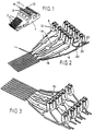
- the connector unit shown in Fig. 1 has eight contact springs 2 protruding at the front end of the connector and being bent-over into their operative positions, see also Fig. 6, in which they are shown in dotted lines in that position.
- the leads of the connector are cast into a plastic block 4, in which the contact springs 2 are, respectively, connected with individual wire connector terminals 6 arranged in two rows with four in each row, viz, a foremost high level row 8 and a rearmost low level row 10.
- Each of these inverted U-shaped terminals is provided with a notch 12 for receiving a horizontally disposed wire end, and on the conductor block 4 they are marked with the uneven figures 1-7 at the higher row 8, and (as indicated in Fig. 3) with the even figures 2-8 at the lower row 10.
- Figs. 2 and 3 show the packing of leads as made ready for being cast into the body 4.
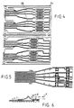
- the leads connecting the wiring terminals in the rear row 10 with their associated contact springs 2 extend in the plane of the forwardly projecting, not yet bent-over contact springs 2, while only the inverted U-shaped terminals 6 are provided as bent-up portions on these leads.
- the other four leads are bent upwardly a short distance at 14, where-after they extend rearwardly through a short horizontal stretch 16 and then further through an upwardly inclined stretch 18 to the inverted U-member forming the associated terminal 6 in the upper terminal row, and therefrom further rearwardly through a downwardly inclined stretch 20 and a following, rear stretch 23 almost in level with the foremost horizontal stretch 16, i.e. somewhat spaced above the level of the lowermost leads.
- the lower terminals 6 have rearwardly projecting portions.
- the lead packing according to Figs. 2 and 3 is made of two superimposed layers made, each, of four leads as illustrated in Fig. 4.
- This figure shows a section of a bronze strip 24, from which is punched, repeatedly, two bottom layers 26 and two top layers 28, which layers are then subjected to spatial shaping for the formation of the terminals 6 and the raised runs 18, 20 of the upper layer. Thereafter, the two different layers are consecutively superimposed and fed to an injection moulding machine, in which they are provided with the block 4 according to Fig. 1.
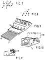
- the immediate result is shown in a more detailed view in Fig. 9, where the contact springs 2 are shown leaving the block 4 horizontally and with their outer ends interconnected by an integral cross strip 3 in each layer. After the moulding of the block 4 these strips are cut off and the springs are bent over according to Fig. 1.
- the unit is provided with a front frame member 5, which is secured by snap locking into non-illustrated apertures in the underside of the foremost flat portion of the block unit.
- a press-cap member 30 which, according to known principles, may facilitate the mounting of the isolated connector wires in the self-cutting type of wiring terminals 6, 12.
- a press-cap member 30 which, according to known principles, may facilitate the mounting of the isolated connector wires in the self-cutting type of wiring terminals 6, 12.
- the electrical conditions are very critical, and instead of prescribing such a mounting, see the wire pair A shown in dot-and-dash lines in Fig. 6, it is found better to arrange the wires as shown by the wire pair B in the same figure, i.e. let in through the top of the presscap 30.
- wires A particularly the uppermost wires, form loops together with the leads of the connector, and it will be noted from Fig. 6 that the areas of these loops will be considerably smaller for wires B than for wires A.
- the wires B are mounted in the press-cap as shown in Fig. 11.
- the connector is made according to a specific standard, according to which the different terminals as numbered 1-8 in Fig. 1 should be used in pairs for different circuits, these pairs being defined by the following terminals: 1-2; 4-5; 3-6; 7-8.
- the associated leads 18 will be located one above the other, such that the loop portion they form will have its cross axis located horizontally or in an oblique plane rather than vertically as in case of leads running in parallel side by side. This is illustrated in Fig. 8, where the two leads a and b form a coil portion having the field axis x.
- Another wire pair c, d is located in a vertical plane, thus having a horizontal loop axis.
- Fig. 7 shows three leads e, f and g arranged in a spatial, triangular pattern. They should be compared with a corresponding flat system, with lead g located in the position marked g'. In that situation the capacity between g' and e, as well as between e and f, may be satisfactory, while it could be desired to increase the capacity between g' and f. In a plane system this will be practically impossible without adversely affecting the other capacities, but if in a spatial system the lead g' is swung along a circle centred in e, it will maintain its capacity to e while increasing its capacity to f. Thus, in position g it still has the desired capacity to e and a capacity to f increased as much as desired.
- e could be swung about g', away from f.
- e may be arranged more or less close to g' for changing even this capacity, and furthermore the widths of the leads will influence the capacities.
- the lead system is provided with various portions such as protrusions 34, Fig. 3, and rear extensions 20, 22 from the upper row of terminals 6, such that these portions can be gripped by suitable transfer means.
- the presence of these electrically non-required portions will call for special attention in the design of the system, because they will inevitably affect at least some of the operationally relevant parameters.
- the connector shown is a female jack or socket member for receiving a counterpart made as a plug with rigid connector terminals. It will be understood that such a plug may be designed widely similar to the disclosed jack or at least according to the same principles with respect to the spatial arrangement of the leads.
- the leads in the lower level extend in a common plane viz.
- the bottom plane also comprising the originally punched-out contact springs 2 according to Figs. 1 and 2, but it will be an open possibility that these leads or some of them might extend otherwise, upwardly or downwardly.
- the row of upper leads which should not necessarily be located in a common plane.
- Even the terminals 6 will not have to be provided in line or level with each other; for the electrical adaptation there could be good reasons for arranging them otherwise, but it will be appreciated that it is indeed practical to have them arranged in neat rows.
- terminals which are potential high-capacity units, can be separated in the longitudinal direction, while in the transverse direction they can be allowed to have a considerable, mechanically required width without making the entire width of the connector element excessive.
- the terminals in the single rows may be non-uniformly interspaced.
- the two or even more rows of wire connection terminals 6 may thus be located otherwise as shown, and so may the contact strips 2, which should not necessarily be arranged in one neat row.
Landscapes
- Details Of Connecting Devices For Male And Female Coupling (AREA)
- Coupling Device And Connection With Printed Circuit (AREA)
- Communication Cables (AREA)
- Small-Scale Networks (AREA)
- Input Circuits Of Receivers And Coupling Of Receivers And Audio Equipment (AREA)
- Filters And Equalizers (AREA)
- Multi-Conductor Connections (AREA)
- Connections Arranged To Contact A Plurality Of Conductors (AREA)
- Structure Of Telephone Exchanges (AREA)
- Insulated Conductors (AREA)
- Cable Transmission Systems, Equalization Of Radio And Reduction Of Echo (AREA)
- Connector Housings Or Holding Contact Members (AREA)
Claims (10)
- Ein Verbindungs- bzw. Anschluß-Buchsen- oder -Steckerelement zur Verwendung in Hochfrequenzkommunikationsnetzwerken, die auf elektrischen Leitern basieren, umfassend eine standardisierte Gruppe Kontaktanschlüsse (2) zur Verbindung mit korrespondierenden Anschlüssen eines Buchsen- bzw. Steckergegenstücks, wobei das Verbindungselement weiter Leitungsverbindungsanschlüsse (6) aufweist, die durch interne Leitungen (14, 16, 18) in dem Buchsen- oder Steckerelement mit den Kontaktanschlüssen verbunden sind, dadurch gekennzeichnet, daß die internen Leitungen der Steckverbindung in einem gegossenen Blockelement (4) aus einem dielektrischen Material in einer räumlichen oder 3-dimensionalen Weise verankert derart angeordnet sind, daß mindestens einige der Leitungen nicht nur seitlich wechselseitig beabstandet sind, sondern auch quer zum seitlichen Abstand, und daß die Leitungen mit Unregelmäßigkeiten, die dem alleinigen Zweck der Optimierung der elektrischen Übertragungsfunktion der Verbindung dienen, geformt und wechselseitig ausgebildet sind.
- Ein Steckverbindungselement nach Anspruch 1, bei dem sich die Leitungen, die sich von den Kontaktanschlüssen nach hinten gerichtet erstrecken, allgemein voneinander weg ausbreiten, wobei sich einige der Leitungen in einer gemeinsamen Ebene erstrecken, in der sie seitlich voneinander divergieren, und andere Leitungen sich in einer divergierenden Weise in einer oder mehreren Ebenen, die von der gemeinsamen Ebene divergieren, erstrecken.
- Ein Steckverbindungselement nach Anspruch 1, bei dem sich die Leitungen zu jeweiligen Leitungsverbindungsanschlüssen, die sich in schrägen Reihen befinden, erstrecken, falls erforderlich mit uneinheitlichen Anschlußbreiten und mit einem Zwischenabstand in jeder Reihe, wobei eine Reihe beabstandet hinter einer anderen und vorzugsweise auch davon beabstandet senkrecht zu der Ebene der Verbindung zwischen den Kontaktanschlüssen und der anderen Reihe der Leitungsverbindungsanschlüsse.
- Ein Steckverbindungselement nach Anspruch 1, bei dem die Leitungen allgemein in zwei Lagen angeordnet sind, wobei die Kontaktanschlüsse jeder Lage bündig und verflochten-mit den Kontaktanschlüssen der anderen Lage verbunden sind, wobei sich die Leitungen in jeder Lage von den Leitungsverbindungsanschlüssen zum hinteren Ende des Verbindungselements rückwärts gerichtet (20, 22, 23) fortsetzen.
- Ein Steckverbindungselement nach Anspruch 4, bei dem sich eine Bodenlage in einer allgemein ebenen Weise erstreckt, ausgenommen nach oben gebogene Leitungsanschlußschleifen nahe dem hinteren Ende des Elements, während sich eine obere Lage allgemein nach oben und nach hinten geneigt über die Bodenlage bis zu einer Reihe integraler Leitungsanschlüsse oberhalb und vor den Leitungsanschlüssen der Bodenlage erstreckt und dann weiter nach hinten und nach unten in Richtung des hinteren Endes des Elements.
- Ein Steckverbindungselement nach Anspruch 1, bei dem sich mindestens eine Leitung, die sich von ihrem zugehörigen Kontaktanschluß nach hinten erstreckt, nach oben von ihrer benachbarten Leitung hervorsteht, dann seitlich zu einer Position oberhalb der benachbarten Leitung und dann nach hinten oberhalb und vertikal divergierend von der benachbarten Leitung.
- Ein Steckverbindungselement Anspruch 3 und umfassend eine Presskappe (30), die betätigbar ist, umjeweilige Leitungsenden aufzunehmen, die durch eine Druckbetätigung der Presskappe über die Anschlüsse nach unten gemeinsam in Kerben in den Leitungsverbindungsanschlüssen montiert werden sollen, wobei die Presskappe auf ihrer oberen Seite mit Leitung-Durchlaßlöchern versehen ist, derart, daß die Leitungsenden in ihrer montierten Position allgemein in einem Bereich zwischen den Anschlußreihen angeordnet sind.
- Ein Steckverbindungselement nach Anspruch 1, bei dem die Leitungen in einem gegossenen Block (4) eines dielektrischen Materials angeordnet sind, und bei dem einige Leitung-Bereichsabschnitte, getrennt von den Anschlüssen, an der Oberfläche des Blocks freiliegen.
- Ein Verfahren zur Herstellung eines Steckverbindungselements nach Anspruch 4, gekennzeichnet durch das Zusammenbringen zweier Lagen von im Endbereich verbundenen, gestanzten Leitungen, von denen eine Lage im wesentlichen eben ist, abgesehen von nach oben gebogenen Leitungsanschlußbereichen auf den einzelnen Leitungen, während für die andere Lage deren Leitungen sich nach oben divergierend von den Leitungen der unteren Lage erstreckt werden, dann die Leitungen miteinander durch Vereinigen in einem injektionsgeschweißten Blockelement verankert und die verbindenden Bereiche zwischen den Leitungsenden weggeschnitten werden.
- Ein Verfahren nach Anspruch 9, wobei die Leitungsverbindungsanschlüsse so angeordnet werden, daß sie in beabstandeten Querreihen angebracht werden, die mit hintersten Querverbindungsbereichen, die schließlich weggeschnitten werden, versehen sind.
Applications Claiming Priority (4)
| Application Number | Priority Date | Filing Date | Title |
|---|---|---|---|
| DK281/93 | 1993-03-12 | ||
| DK28193 | 1993-03-12 | ||
| DK93281A DK28193D0 (da) | 1993-03-12 | 1993-03-12 | Forbindelsesstik til kommunikationsnet |
| PCT/DK1994/000107 WO1994021007A1 (en) | 1993-03-12 | 1994-03-11 | A connector element for telecommunication |
Publications (2)
| Publication Number | Publication Date |
|---|---|
| EP0688472A1 EP0688472A1 (de) | 1995-12-27 |
| EP0688472B1 true EP0688472B1 (de) | 2000-05-17 |
Family
ID=8091795
Family Applications (1)
| Application Number | Title | Priority Date | Filing Date |
|---|---|---|---|
| EP94908996A Expired - Lifetime EP0688472B1 (de) | 1993-03-12 | 1994-03-11 | Telekommunikationssteckverbinder |
Country Status (12)
| Country | Link |
|---|---|
| US (1) | US6113418A (de) |
| EP (1) | EP0688472B1 (de) |
| JP (1) | JP3414737B2 (de) |
| AT (1) | ATE193164T1 (de) |
| AU (1) | AU691485B2 (de) |
| CA (1) | CA2157279C (de) |
| DE (1) | DE69424536T2 (de) |
| DK (2) | DK28193D0 (de) |
| ES (1) | ES2149261T3 (de) |
| NZ (1) | NZ260078A (de) |
| TW (1) | TW250595B (de) |
| WO (1) | WO1994021007A1 (de) |
Families Citing this family (38)
| Publication number | Priority date | Publication date | Assignee | Title |
|---|---|---|---|---|
| US5586914A (en) * | 1995-05-19 | 1996-12-24 | The Whitaker Corporation | Electrical connector and an associated method for compensating for crosstalk between a plurality of conductors |
| JPH097651A (ja) * | 1995-06-09 | 1997-01-10 | Minnesota Mining & Mfg Co <3M> | 接触子及びこの接触子を備えた端末コネクタ |
| JP3354373B2 (ja) | 1995-12-25 | 2002-12-09 | 松下電工株式会社 | モジュラジャック |
| AU716436B2 (en) * | 1995-12-25 | 2000-02-24 | Matsushita Electric Works Ltd. | Connector |
| JP3354371B2 (ja) | 1995-12-25 | 2002-12-09 | 松下電工株式会社 | コネクタ |
| FR2757691B1 (fr) * | 1996-12-20 | 1999-01-22 | Pouyet Sa | Procede de realisation d'une reglette d'interconnexion de lignes telephoniques ou informatiques, et reglette obtenue par ce procede |
| US5993259A (en) * | 1997-02-07 | 1999-11-30 | Teradyne, Inc. | High speed, high density electrical connector |
| CH693012A5 (de) * | 1997-06-02 | 2003-01-15 | Reichle & De Massari Fa | Steckverbindungsteil für hochfrequente Datenübertragung über elektrische Leiter. |
| GB2332786B (en) * | 1997-11-04 | 2001-10-10 | Richard Weatherley | Plug and mating socket for data transmission systems |
| US6346005B1 (en) * | 1998-01-19 | 2002-02-12 | The Siemon Company | Reduced cross-talk high frequency wiring connection system |
| US6086428A (en) * | 1998-03-25 | 2000-07-11 | Lucent Technologies Inc. | Crosstalk compensation for connector jack |
| CH695034A5 (de) * | 1998-09-30 | 2005-11-15 | Reichle & De Massari Fa | Steckverbindungsteil einer Steckverbindung fuer hochfrequente Datenuebertragung ueber elektrische Leiter. |
| US6409547B1 (en) | 1998-12-02 | 2002-06-25 | Nordx/Cdt, Inc. | Modular connectors with compensation structures |
| US6468090B2 (en) * | 1999-09-15 | 2002-10-22 | Fci Americas Technology, Inc. | Low inductance power connector and method of reducing inductance in an electrical connector |
| US6290524B1 (en) * | 2000-07-12 | 2001-09-18 | Molex Incorporated | System for varying capacitive coupling between electrical terminals |
| US6896557B2 (en) | 2001-03-28 | 2005-05-24 | Ortronics, Inc. | Dual reactance low noise modular connector insert |
| US7172466B2 (en) * | 2001-04-05 | 2007-02-06 | Ortronics, Inc. | Dual reactance low noise modular connector insert |
| US20030082954A1 (en) * | 2001-11-01 | 2003-05-01 | Espenshade Leonard K. | Cross-talk reduced modular jack |
| CA2464834A1 (en) | 2004-04-19 | 2005-10-19 | Nordx/Cdt Inc. | Connector |
| US7530854B2 (en) * | 2006-06-15 | 2009-05-12 | Ortronics, Inc. | Low noise multiport connector |
| US7288001B1 (en) | 2006-09-20 | 2007-10-30 | Ortronics, Inc. | Electrically isolated shielded multiport connector assembly |
| US7485010B2 (en) * | 2007-06-14 | 2009-02-03 | Ortronics, Inc. | Modular connector exhibiting quad reactance balance functionality |
| JP4795444B2 (ja) * | 2009-02-09 | 2011-10-19 | ホシデン株式会社 | コネクタ |
| US8366485B2 (en) | 2009-03-19 | 2013-02-05 | Fci Americas Technology Llc | Electrical connector having ribbed ground plate |
| JP5112383B2 (ja) * | 2009-05-28 | 2013-01-09 | ヒロセ電機株式会社 | モジュラープラグ |
| US8231415B2 (en) | 2009-07-10 | 2012-07-31 | Fci Americas Technology Llc | High speed backplane connector with impedance modification and skew correction |
| US9088116B2 (en) | 2011-11-23 | 2015-07-21 | Panduit Corp. | Compensation network using an orthogonal compensation network |
| EP2624034A1 (de) | 2012-01-31 | 2013-08-07 | Fci | Abbaubare optische Kupplungsvorrichtung |
| USD727852S1 (en) | 2012-04-13 | 2015-04-28 | Fci Americas Technology Llc | Ground shield for a right angle electrical connector |
| USD727268S1 (en) | 2012-04-13 | 2015-04-21 | Fci Americas Technology Llc | Vertical electrical connector |
| US9257778B2 (en) | 2012-04-13 | 2016-02-09 | Fci Americas Technology | High speed electrical connector |
| USD718253S1 (en) | 2012-04-13 | 2014-11-25 | Fci Americas Technology Llc | Electrical cable connector |
| US8944831B2 (en) | 2012-04-13 | 2015-02-03 | Fci Americas Technology Llc | Electrical connector having ribbed ground plate with engagement members |
| USD751507S1 (en) | 2012-07-11 | 2016-03-15 | Fci Americas Technology Llc | Electrical connector |
| US9543703B2 (en) | 2012-07-11 | 2017-01-10 | Fci Americas Technology Llc | Electrical connector with reduced stack height |
| USD745852S1 (en) | 2013-01-25 | 2015-12-22 | Fci Americas Technology Llc | Electrical connector |
| USD720698S1 (en) | 2013-03-15 | 2015-01-06 | Fci Americas Technology Llc | Electrical cable connector |
| DE112014005378T5 (de) * | 2013-11-26 | 2016-08-11 | Samtec, Inc. | Direktbefestigungsverbinder |
Family Cites Families (9)
| Publication number | Priority date | Publication date | Assignee | Title |
|---|---|---|---|---|
| US4418239A (en) * | 1981-08-24 | 1983-11-29 | Oak Industries Inc. | Flexible connector with interconnection between conductive traces |
| DE3607409C1 (de) * | 1986-03-06 | 1987-06-11 | Allied Corp | Steckverbinder fuer Flachkabelanschluss |
| JPH01315968A (ja) * | 1988-03-07 | 1989-12-20 | Hirose Electric Co Ltd | 電気コネクタ |
| US4995828A (en) * | 1990-04-12 | 1991-02-26 | Itt Corporation | Connector for paired wire cable |
| US5064383A (en) * | 1990-11-14 | 1991-11-12 | Amp Incorporated | Multiple conductor cable connector with clip and towers |
| US5186647A (en) * | 1992-02-24 | 1993-02-16 | At&T Bell Laboratories | High frequency electrical connector |
| US5299956B1 (en) * | 1992-03-23 | 1995-10-24 | Superior Modular Prod Inc | Low cross talk electrical connector system |
| US5326286A (en) * | 1992-12-17 | 1994-07-05 | Molex Incorporated | Electrical connector assembly with terminal alignment system |
| US5586914A (en) * | 1995-05-19 | 1996-12-24 | The Whitaker Corporation | Electrical connector and an associated method for compensating for crosstalk between a plurality of conductors |
-
1993
- 1993-03-12 DK DK93281A patent/DK28193D0/da not_active Application Discontinuation
-
1994
- 1994-03-11 JP JP51949094A patent/JP3414737B2/ja not_active Expired - Lifetime
- 1994-03-11 AU AU62033/94A patent/AU691485B2/en not_active Expired
- 1994-03-11 DE DE69424536T patent/DE69424536T2/de not_active Expired - Lifetime
- 1994-03-11 ES ES94908996T patent/ES2149261T3/es not_active Expired - Lifetime
- 1994-03-11 EP EP94908996A patent/EP0688472B1/de not_active Expired - Lifetime
- 1994-03-11 DK DK94908996T patent/DK0688472T3/da active
- 1994-03-11 US US08/530,266 patent/US6113418A/en not_active Expired - Lifetime
- 1994-03-11 NZ NZ260078A patent/NZ260078A/en not_active IP Right Cessation
- 1994-03-11 WO PCT/DK1994/000107 patent/WO1994021007A1/en not_active Ceased
- 1994-03-11 AT AT94908996T patent/ATE193164T1/de not_active IP Right Cessation
- 1994-03-11 CA CA002157279A patent/CA2157279C/en not_active Expired - Lifetime
- 1994-05-04 TW TW083104028A patent/TW250595B/zh active
Also Published As
| Publication number | Publication date |
|---|---|
| AU6203394A (en) | 1994-09-26 |
| CA2157279A1 (en) | 1994-09-15 |
| ES2149261T3 (es) | 2000-11-01 |
| DK28193D0 (da) | 1993-03-12 |
| WO1994021007A1 (en) | 1994-09-15 |
| EP0688472A1 (de) | 1995-12-27 |
| DE69424536D1 (de) | 2000-06-21 |
| ATE193164T1 (de) | 2000-06-15 |
| CA2157279C (en) | 2004-08-10 |
| AU691485B2 (en) | 1998-05-21 |
| DE69424536T2 (de) | 2001-02-15 |
| JPH08507406A (ja) | 1996-08-06 |
| DK0688472T3 (da) | 2000-10-09 |
| TW250595B (de) | 1995-07-01 |
| NZ260078A (en) | 1997-06-24 |
| US6113418A (en) | 2000-09-05 |
| JP3414737B2 (ja) | 2003-06-09 |
Similar Documents
| Publication | Publication Date | Title |
|---|---|---|
| EP0688472B1 (de) | Telekommunikationssteckverbinder | |
| US6102730A (en) | Connector element for telecommunications | |
| JP4168158B2 (ja) | 改良コネクター | |
| CA2243149C (en) | High-frequency communication jack | |
| CA2244426C (en) | Solderless mountable insulation displacement connector | |
| CA2244301C (en) | Wire terminal block for communication connectors | |
| US7448920B2 (en) | Wire lead guide and method for terminating a communications cable | |
| KR100668189B1 (ko) | 전기플러그-소켓 접속부로 이루어진 접속케이블 | |
| AU741508B2 (en) | Alignment apparatus for use in the jack interface housing of a communication plug | |
| JP2001506394A (ja) | 電気コネクタ及びそれに関わる複数の導体間のクロストークを補償する方法 | |
| EP1365486B1 (de) | Modularer Jack Steckverbinder | |
| AU8302998A (en) | Strain relief apparatus for use in a communication plug | |
| JPH11508723A (ja) | パッチコード組立体 | |
| AU8303298A (en) | Communication plug | |
| GB2347025A (en) | Wiring unit with angled insulation displacement contacts | |
| US6276954B1 (en) | Communication plug having consistent and set levels of complementary crosstalk | |
| JP2002508882A (ja) | 高速idcモジュラジャック | |
| US6488525B2 (en) | Wire lead guide for communication connectors | |
| US20010024902A1 (en) | Modular plug and harnessed plug | |
| AU764903B2 (en) | A connector element for telecommunication | |
| JP2568405B2 (ja) | ケ−ブル用多対コネクタ | |
| RO119800B1 (ro) | Conector | |
| CN216598023U (zh) | 一种高密度配线架及其idc模块 | |
| CA2712846C (en) | Wire lead guide and method for terminating a communications cable | |
| AU752830B2 (en) | Low-crosstalk electrical connector grouping like conductors together |
Legal Events
| Date | Code | Title | Description |
|---|---|---|---|
| PUAI | Public reference made under article 153(3) epc to a published international application that has entered the european phase |
Free format text: ORIGINAL CODE: 0009012 |
|
| 17P | Request for examination filed |
Effective date: 19950918 |
|
| AK | Designated contracting states |
Kind code of ref document: A1 Designated state(s): AT BE CH DE DK ES FR GB GR IE IT LI NL PT SE |
|
| GRAG | Despatch of communication of intention to grant |
Free format text: ORIGINAL CODE: EPIDOS AGRA |
|
| 17Q | First examination report despatched |
Effective date: 19970822 |
|
| GRAG | Despatch of communication of intention to grant |
Free format text: ORIGINAL CODE: EPIDOS AGRA |
|
| GRAH | Despatch of communication of intention to grant a patent |
Free format text: ORIGINAL CODE: EPIDOS IGRA |
|
| GRAH | Despatch of communication of intention to grant a patent |
Free format text: ORIGINAL CODE: EPIDOS IGRA |
|
| RAP1 | Party data changed (applicant data changed or rights of an application transferred) |
Owner name: CEKAN/CDT A/S |
|
| RIN1 | Information on inventor provided before grant (corrected) |
Inventor name: KJERDAHL, POUL |
|
| GRAA | (expected) grant |
Free format text: ORIGINAL CODE: 0009210 |
|
| AK | Designated contracting states |
Kind code of ref document: B1 Designated state(s): AT BE CH DE DK ES FR GB GR IE IT LI NL PT SE |
|
| PG25 | Lapsed in a contracting state [announced via postgrant information from national office to epo] |
Ref country code: NL Free format text: LAPSE BECAUSE OF FAILURE TO SUBMIT A TRANSLATION OF THE DESCRIPTION OR TO PAY THE FEE WITHIN THE PRESCRIBED TIME-LIMIT Effective date: 20000517 Ref country code: LI Free format text: LAPSE BECAUSE OF FAILURE TO SUBMIT A TRANSLATION OF THE DESCRIPTION OR TO PAY THE FEE WITHIN THE PRESCRIBED TIME-LIMIT Effective date: 20000517 Ref country code: GR Free format text: LAPSE BECAUSE OF NON-PAYMENT OF DUE FEES Effective date: 20000517 Ref country code: CH Free format text: LAPSE BECAUSE OF FAILURE TO SUBMIT A TRANSLATION OF THE DESCRIPTION OR TO PAY THE FEE WITHIN THE PRESCRIBED TIME-LIMIT Effective date: 20000517 Ref country code: BE Free format text: LAPSE BECAUSE OF FAILURE TO SUBMIT A TRANSLATION OF THE DESCRIPTION OR TO PAY THE FEE WITHIN THE PRESCRIBED TIME-LIMIT Effective date: 20000517 Ref country code: AT Free format text: LAPSE BECAUSE OF FAILURE TO SUBMIT A TRANSLATION OF THE DESCRIPTION OR TO PAY THE FEE WITHIN THE PRESCRIBED TIME-LIMIT Effective date: 20000517 |
|
| REF | Corresponds to: |
Ref document number: 193164 Country of ref document: AT Date of ref document: 20000615 Kind code of ref document: T |
|
| RIC1 | Information provided on ipc code assigned before grant |
Free format text: 7H 01R 13/719 A, 7H 01R 12/24 B, 7H 04B 3/32 B |
|
| RIN1 | Information on inventor provided before grant (corrected) |
Inventor name: KJELDAHL, POUL |
|
| REG | Reference to a national code |
Ref country code: IE Ref legal event code: FG4D Ref country code: CH Ref legal event code: EP |
|
| REF | Corresponds to: |
Ref document number: 69424536 Country of ref document: DE Date of ref document: 20000621 |
|
| ITF | It: translation for a ep patent filed | ||
| PG25 | Lapsed in a contracting state [announced via postgrant information from national office to epo] |
Ref country code: SE Free format text: LAPSE BECAUSE OF FAILURE TO SUBMIT A TRANSLATION OF THE DESCRIPTION OR TO PAY THE FEE WITHIN THE PRESCRIBED TIME-LIMIT Effective date: 20000817 Ref country code: PT Free format text: LAPSE BECAUSE OF FAILURE TO SUBMIT A TRANSLATION OF THE DESCRIPTION OR TO PAY THE FEE WITHIN THE PRESCRIBED TIME-LIMIT Effective date: 20000817 |
|
| ET | Fr: translation filed | ||
| REG | Reference to a national code |
Ref country code: DK Ref legal event code: T3 |
|
| NLV1 | Nl: lapsed or annulled due to failure to fulfill the requirements of art. 29p and 29m of the patents act | ||
| REG | Reference to a national code |
Ref country code: ES Ref legal event code: FG2A Ref document number: 2149261 Country of ref document: ES Kind code of ref document: T3 |
|
| REG | Reference to a national code |
Ref country code: CH Ref legal event code: PL |
|
| PG25 | Lapsed in a contracting state [announced via postgrant information from national office to epo] |
Ref country code: IE Free format text: LAPSE BECAUSE OF NON-PAYMENT OF DUE FEES Effective date: 20010312 |
|
| PLBE | No opposition filed within time limit |
Free format text: ORIGINAL CODE: 0009261 |
|
| STAA | Information on the status of an ep patent application or granted ep patent |
Free format text: STATUS: NO OPPOSITION FILED WITHIN TIME LIMIT |
|
| 26N | No opposition filed | ||
| REG | Reference to a national code |
Ref country code: GB Ref legal event code: IF02 |
|
| REG | Reference to a national code |
Ref country code: IE Ref legal event code: MM4A |
|
| PG25 | Lapsed in a contracting state [announced via postgrant information from national office to epo] |
Ref country code: IT Free format text: LAPSE BECAUSE OF NON-PAYMENT OF DUE FEES Effective date: 20100311 |
|
| PGRI | Patent reinstated in contracting state [announced from national office to epo] |
Ref country code: IT Effective date: 20110616 |
|
| PGFP | Annual fee paid to national office [announced via postgrant information from national office to epo] |
Ref country code: IT Payment date: 20120326 Year of fee payment: 19 |
|
| PGFP | Annual fee paid to national office [announced via postgrant information from national office to epo] |
Ref country code: DK Payment date: 20130325 Year of fee payment: 20 Ref country code: GB Payment date: 20130327 Year of fee payment: 20 Ref country code: DE Payment date: 20130327 Year of fee payment: 20 Ref country code: ES Payment date: 20130326 Year of fee payment: 20 Ref country code: FR Payment date: 20130405 Year of fee payment: 20 |
|
| REG | Reference to a national code |
Ref country code: DE Ref legal event code: R071 Ref document number: 69424536 Country of ref document: DE |
|
| REG | Reference to a national code |
Ref country code: DK Ref legal event code: EUP Effective date: 20140311 |
|
| REG | Reference to a national code |
Ref country code: GB Ref legal event code: PE20 Expiry date: 20140310 |
|
| PG25 | Lapsed in a contracting state [announced via postgrant information from national office to epo] |
Ref country code: DE Free format text: LAPSE BECAUSE OF EXPIRATION OF PROTECTION Effective date: 20140312 Ref country code: GB Free format text: LAPSE BECAUSE OF EXPIRATION OF PROTECTION Effective date: 20140310 |
|
| REG | Reference to a national code |
Ref country code: ES Ref legal event code: FD2A Effective date: 20140926 |
|
| PG25 | Lapsed in a contracting state [announced via postgrant information from national office to epo] |
Ref country code: ES Free format text: LAPSE BECAUSE OF EXPIRATION OF PROTECTION Effective date: 20140312 |