EP0686324B1 - Empfänger mit regelbarem bandpassfilter - Google Patents
Empfänger mit regelbarem bandpassfilter Download PDFInfo
- Publication number
- EP0686324B1 EP0686324B1 EP95901574A EP95901574A EP0686324B1 EP 0686324 B1 EP0686324 B1 EP 0686324B1 EP 95901574 A EP95901574 A EP 95901574A EP 95901574 A EP95901574 A EP 95901574A EP 0686324 B1 EP0686324 B1 EP 0686324B1
- Authority
- EP
- European Patent Office
- Prior art keywords
- resistive
- receiver
- current
- frequency
- passive filtering
- Prior art date
- Legal status (The legal status is an assumption and is not a legal conclusion. Google has not performed a legal analysis and makes no representation as to the accuracy of the status listed.)
- Expired - Lifetime
Links
Images

Classifications
-
- H—ELECTRICITY
- H04—ELECTRIC COMMUNICATION TECHNIQUE
- H04M—TELEPHONIC COMMUNICATION
- H04M3/00—Automatic or semi-automatic exchanges
-
- H—ELECTRICITY
- H03—ELECTRONIC CIRCUITRY
- H03J—TUNING RESONANT CIRCUITS; SELECTING RESONANT CIRCUITS
- H03J5/00—Discontinuous tuning; Selecting predetermined frequencies; Selecting frequency bands with or without continuous tuning in one or more of the bands, e.g. push-button tuning, turret tuner
- H03J5/24—Discontinuous tuning; Selecting predetermined frequencies; Selecting frequency bands with or without continuous tuning in one or more of the bands, e.g. push-button tuning, turret tuner with a number of separate pretuned tuning circuits or separate tuning elements selectively brought into circuit, e.g. for waveband selection or for television channel selection
- H03J5/246—Discontinuous tuning; Selecting predetermined frequencies; Selecting frequency bands with or without continuous tuning in one or more of the bands, e.g. push-button tuning, turret tuner with a number of separate pretuned tuning circuits or separate tuning elements selectively brought into circuit, e.g. for waveband selection or for television channel selection using electronic means
-
- H—ELECTRICITY
- H03—ELECTRONIC CIRCUITRY
- H03H—IMPEDANCE NETWORKS, e.g. RESONANT CIRCUITS; RESONATORS
- H03H19/00—Networks using time-varying elements, e.g. N-path filters
-
- H—ELECTRICITY
- H04—ELECTRIC COMMUNICATION TECHNIQUE
- H04B—TRANSMISSION
- H04B1/00—Details of transmission systems, not covered by a single one of groups H04B3/00 - H04B13/00; Details of transmission systems not characterised by the medium used for transmission
- H04B1/06—Receivers
- H04B1/16—Circuits
- H04B1/30—Circuits for homodyne or synchrodyne receivers
-
- H—ELECTRICITY
- H04—ELECTRIC COMMUNICATION TECHNIQUE
- H04B—TRANSMISSION
- H04B1/00—Details of transmission systems, not covered by a single one of groups H04B3/00 - H04B13/00; Details of transmission systems not characterised by the medium used for transmission
- H04B1/06—Receivers
- H04B1/16—Circuits
- H04B1/26—Circuits for superheterodyne receivers
- H04B1/28—Circuits for superheterodyne receivers the receiver comprising at least one semiconductor device having three or more electrodes
Definitions
- the present invention relates to a radio frequency receiver and particularly but not exclusively to an adjustable bandwidth filter for use in a radio frequency receiver for receiving particularly, but not exclusively, digital signals.
- Communication receivers for receiving digital signals are well known and frequently have an architecture in which a received signal is applied to an adjustable gain r.f. amplifier prior to a first frequency down conversion stage which produces an i.f. frequency.
- the i.f. frequency is filtered in say a SAW filter and the filtered signal is applied to another frequency down conversion stage in which the i.f. signal is applied to nominally quadrature related mixers, the outputs of which are low pass filtered and then applied to a digital signal processor (DSP).
- DSP digital signal processor
- Figure 1 illustrates a typical low pass filter input-output characteristic in which the ordinate is amplitude in db and the abscissa is frequency f.
- the wanted signal band is indicated as f w and the unwanted higher band of frequencies is indicated as f uw .
- the receiver noise level is indicated by a horizontal broken line RNL.
- the amplitude of the input signal need only be several dbs above a level termed the Minimum Distinguishable Signal MDS. Accordingly there is little point in designing filters to handle much bigger signals if the result is the consumption of a lot more current.
- the low pass filters are thus generally designed to handle a limited dynamic range of wanted signals and to consume a low power.
- a problem arises when strong unwanted signals need to be blocked by the filters as there is no AGC applied by the DSP.
- the filters must be able to cope with such unwanted signals in a linear way. If the filters are designed to be capable of handling large unwanted signals this could lead to a significant increase in power consumption, for example 141 times more power could be required for handling an unwanted signal which is greater than the MDS level by 23 db than for a signal just above that level.
- Such low pass filters are not infrequently voltage driven transconductor filters.
- a much larger signal for example 14.5 db larger in the case of a Gaussian to 6 db filter, can occur in the stop-band than in the wanted band without the filter going non-linear.
- Even with this improvement there is still a desire to cope with an even larger signal, for example up to say 23 db larger, in the stop-band without the filter going non-linear and also to make the filter have an adjustable bandwidth to be able to selectively pass a narrow band signal which for example occurs in the Pan-European or GSM cellular telephone system and a wider band signal which for example occurs in the Digital European Cordless Telephone (DECT) system.
- DECT Digital European Cordless Telephone
- a radio frequency receiver comprising a frequency down conversion stage which includes first passive filtering means having a first cut-off frequency, first and second outputs from the frequency down conversion stage, an amplifier comprising first and second active devices having control electrodes connected to the first and second outputs, current supply electrodes and current output electrodes, third filtering means having inputs for receiving current outputs from said first and second active devices, said third filtering means including transconducting means connected to said inputs, first resistive means interconnecting the current supply electrodes of the first and second active devices, and second passive filtering means including a resistive component and switching means, whereby when the switching means are closed the resistive component shunts the first resistive means and the amplifier has a wider bandwidth than when the switching means are open circuit.
- the level of signal in the stop band which can be handled without the filter going non-linear is increased from 14.5 db to 23 db without increasing the current consumption.
- the provision of the second passive filtering means enables the filter bandwidth to be selectively adjustable.
- the second passive filtering means may further comprise a first capacitance.
- the resistive component may comprise second and third resistance means of substantially equal resistance value, each of the second and third resistive means having first and second ends, the first ends being coupled to respective ends of the first resistive means.
- the switching means may comprise first and second switching means coupled respectively between the second ends of the second and third resistive means and the first capacitance means.
- the first and second switching means may comprise field effect transistors and by locating them between the second and third resistive means and the capacitive means it is possible to operate the switching means using relatively small d.c. voltages and minimise non-linearities due to differences in potential between the first switching means and the substrate and the second switching means and the substrate. Also using two switching means rather than one maintains the symmetry of the circuit and in so doing avoids the risk of introducing other non-linearities.
- An advantage of arranging the second passive filtering means to be connected in parallel with the first resistive means when selecting the wider band signals is that the narrow band signal is not compromised because the second and third switching means are then open (non-conductive) and the non-linearities are not present.
- the receiver comprises an antenna 10 which is connected to an r.f. input stage 12 comprising adjustable gain r.f. amplifiers 14,15 and a mixer 16 connected in cascade and a first local oscillator 18 connected to the mixer 16.
- the products of mixing are supplied to a band pass filter 20 which selects the desired band of intermediate frequencies (i.f.).
- a second frequency down conversion stage 22 is coupled to an output of the filter 20.
- the stage 22 comprises an i.f. amplifier 24 and two nominally quadrature related signal paths I and Q which are connected to inputs of a DSP 26.
- Each of the I and Q signal paths comprises a mixer 28,29 having an input coupled to an output of the amplifier 24 and an adjustable bandwidth low pass filter 30,31 coupled between its mixer 28,29, respectively, and the DSP 26.
- the nominally quadrature related signal paths I and Q are obtained in the illustrated receiver by supplying a local oscillator signal nominally in quadrature to the mixers 28,29. This is done by connecting an output of a local oscillator 32 directly to the mixer 28 and to a nominally ⁇ /2 phase shifter 34 having an output connected to the mixer 29.
- the DSP 26 not only is used to recover the signal but also is used to control the gain of one or both r.f. amplifiers 14,15 so that the amplitude of the wanted signal f w ( Figure 1) is only slightly greater than the MDS level.
- the operation of this type of receiver is generally well known and has been summarised in the preamble of this specification.
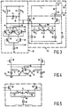
- FIG 3 illustrates an embodiment of a mixer 28 and a low pass filter 30 having a switchable bandwidth.
- the mixer 28 comprises a first long tail pair circuit formed by NPN transistors 36,37 whose base electrodes receive an input signal from the amplifier 24 ( Figure 2) and whose emitter electrodes are jointly connected to a current source 38.
- the collector electrodes of the transistors 36,37 are respectively connected to second and third long tail pair circuits formed by pairs of NPN transistors 40,41 and 42,43.
- the emitter electrodes of the pairs of transistors 40,41 and 42,43 are respectively connected to the collector electrodes of the transistors 36,37.
- the base electrodes of the transistors 40,43 are interconnected as are the base electrodes of the transistors 41,42.
- a local oscillator (LO) source is connected to the respective interconnections.
- the collector electrodes of the transistors 40,42 and of the transistors 41,43 are interconnected at junctions 44,46, respectively.
- the junctions 44,46 are coupled to a supply rail V + by way of a first passive filtering means 48 formed by resistive devices 50,51 of substantially equal value connected respectively between the junctions 44,46 and the supply line V + and a shunt capacitor 52.
- the partially filtered output voltages appearing at the junctions 44,46 are supplied to a post mixer amplifier consisting of a voltage to current converter 54 comprising NPN transistors 56,58 whose base electrodes are connected respectively to the junctions 44,46, whose emitter electrodes are interconnected by an emitter degeneration resistive device 60 and are connected to respective current sources 62,64, and whose collector electrodes are connected to respective inputs 65,67 of a current driven transconductor filter 66 to be described with reference to Figure 6.
- a second, switchable passive filtering means 68 is connectable in parallel with the resistive device 60.
- the filtering means comprises two substantially equal value resistive devices 70,71 having one end connected respectively to the emitter electrodes of the transistors 56,58, a capacitive element 74 and switch devices 72,73 connected between the second ends of the resistive devices 70,71, respectively and respective plates of the capacitive element 74.
- Figure 4 illustrates an embodiment in which the switch devices 72,73 comprise field effect transistors, the gate electrodes of which are connected to a bandwidth control input 75.
- the switch devices 72,73 are non-conductive when the second passive filtering means 68 is non-operative and the overall circuit is behaving as a narrow band filter and conductive, in response to a signal on the input 75, when the second passive filtering means 68 is shunting the resistive device 60 to provide a broader bandwidth filter.
- Figure 5 is a variant of the voltage to current converter 54 in which the current sources 62,64 are combined into one current source 63 which is connected to a centre tap of the resistor 60.
- the current driven transconductor low pass filter 66 ( Figure 6) comprises a transconductor 76 configured as a resistor connected between the inputs 65,67, a simulation of an LC filter comprising two series connected inductances 78,79 and three shunt capacitive elements 80,81,82 and a transconductor 84 configured as a resistor connected to outputs 85,86.
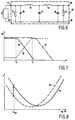
- FIG. 7 illustrates how the second, switchable passive filtering means can be used to widen the filter response.
- the filter response 88 is that shown by the continuous line and is produced by the first passive filtering means.
- the response is a narrow band response having a cut-off above a wanted frequency f a but below the frequency f b of the alternative wanted broadband signal.
- the second, switchable passive filtering means modifies the normally frequency independent response of the voltage to current converter 54 so that it has the response 90 shown in broken lines.
- an overall broadband filter response 92 shown in chain-dot lines is thus obtained.
- two switch devices 72,73 are provided in order to maintain symmetry and thereby avoid introducing non-linearities.
- these devices 72,73 By arranging these devices 72,73 to be on either side of the capacitive element 74 then the effect of voltage variations with respect to the substrate are very small or substantially zero.
- the switch devices 72,73 were located on the other sides of the resistive elements 70,71 then the effect of voltage variations with respect to the substrate will be much larger which is undesirable.
- the frequency increases the voltage across the capacitive element 74 goes down thereby causing the switch devices 72,73 to get closer together, differences in the influence of the substrate on the on-resistance diminishing.
- the curve 94 shown by a full line is the typical noise characteristic of an amplifier. This characteristic has a minima which indicates the value of the source resistance Rs which gives the best noise figure.
- the voltage to current converter 54 sees the output resistance (Rs 28 ) of the mixer 28 which is less than the optimum value. This is normally the case and is a consequence of the resistive device 60 being relatively large so that the linearity of the voltage to current converter 54 is adequate.
- the optimum value of Rs would typically be hundreds of kilohms.
- the signal to noise ratio at the input to the voltage to current converter 54 remains substantially unchanged, in other words the amplitude of the mixer output and the noise figure effectively track each other.
- the cut-off frequency of the current driven transconductor filter 66 can also be tuned from f a to f b in known manner.
- Radio receiver suitable for digital cellular and/or digital cordless telephones are provided.
Landscapes
- Engineering & Computer Science (AREA)
- Signal Processing (AREA)
- Computer Networks & Wireless Communication (AREA)
- Superheterodyne Receivers (AREA)
- Networks Using Active Elements (AREA)
Claims (8)
- Funkfrequenzempfänger mit einer Frequenzabwärtsmischstufe (28), die erste passive Filtermittel (50, 51, 52) mit einer ersten Grenzfrequenz (fa), mit einem ersten und einem zweiten Ausgang (44, 46) der Frequenzabwärtsmischstufe aufweist, mit einem Verstärker (54) mit einer ersten und einer zweiten aktiven Anordnung (56, 58), wobei deren Steuerelektroden mit dem ersten und dem zweiten Ausgang, mit Stromzuliefungserelektroden und Stromausgangselektroden verbunden sind, wobei dritte Filtermittel (66) mit Eingängen (65, 67)versehen sind zum Empfangen von Stromausgängen von der genannten ersten und zweiten aktiven Anordnung, wobei die genannten dritten Filtermittel mit den genannten Eingängen verbundene Transkonduktormittel (76) aufweisen, wobei erste Widerstandsmittel (60 die Stromzulieferungselektroden der ersten und der zweiten aktiven Anordnung miteinander verbinden und wobei zweite passive Filtermittel (68) ein Widerstandselement (70, 71) und Schaltmittel (72, 73) umfassen, wodurch, wenn die Schaltmittel geschlossen werden, das Widerstandselement die ersten Widerstandsmittel parallel schalten und der Verstärker eine größere Bandbreite hat als wenn die Schaltmittel offen sind.
- Empfänger nach Anspruch 1, dadurch gekennzeichnet, dass die zweiten passiven Filtermittel weiterhin eine erste Kapazität )74) aufweisen, dass das Widerstandselement zweite und dritte Widerstandselemente (70, 71) nahezu gleichen Wertes aufweisen, wobei jedes Widerstandsmittel der zweiten und dritten Widerstandsmittel ein erstes und ein zweites Ende hat, wobei die ersten Enden mit den betreffenden Enden des ersten Widerstandsmittel (60) gekoppelt sind und dass die Schaltmittel erste und zweite Schaltmittel (72, 73) aufweisen, die zwischen den zweiten Enden der zweiten und dritten Widerstandsmittel (70, 71) und den ersten Widerstandsmitteln vorgesehen sind.
- Empfänger nach Anspruch 2, dadurch gekennzeichnet, dass die ersten und zweiten Schaltmittel (72, 73) Feldeffekttransistoren aufweisen.
- Empfänger nach Anspruch 2 oder 3, dadurch gekennzeichnet, dass der gesamte Widerstandswert des zweiten und dritten Widerstandsmittel kleiner ist als der Widerstandswert des genannten ersten Widerstandsmittels.
- Empfänger nach einem der Ansprüche 2 bis 4, dadurch gekennzeichnet, dass Stromquellen (62, 64) mit jedem der durch die ersten Enden der zweiten und dritten Widerstandsmittel und die Enden des ersten Widerstandsmittels gebildeten Knotenpunkte verbunden sind.
- Empfänger nach einem der Ansprüche 1 bis 4, dadurch gekennzeichnet, dass da erste Widerstandsmittel (60) einen Abgriff hat und dass eine Stromquelle (63) mit dem Abgriff verbunden ist.
- Empfänger nach einem der Ansprüche 1 bis 6, dadurch gekennzeichnet, dass das erste passive Filtermittel nahezu gleichwertige vierte und fünfte Widerstandsmittel (50, 51) aufweist, die zwischen dem ersten und dem zweiten Ausgang (44, 46) der Frequenzabwärtsmischstufe (28) und einer Speiseleitung vorgesehen sind und dass es ein zweites kapazitives Mittel (52) aufweist, das zu dem vierten und fünften Widerstandsmittel parallel geschaltet ist.
- Empfänger nach einem der Ansprüche 1 bis 7, dadurch gekennzeichnet, dass Elemente der ersten und zweiten passiven Filtermittel aus dem gleichen Material hergestellt sind.
Applications Claiming Priority (3)
| Application Number | Priority Date | Filing Date | Title |
|---|---|---|---|
| GB9326464 | 1993-12-24 | ||
| GB939326464A GB9326464D0 (en) | 1993-12-24 | 1993-12-24 | Receiver having an adjustable bandwidth filter |
| PCT/IB1994/000415 WO1995019073A2 (en) | 1993-12-24 | 1994-12-13 | Receiver having an adjustable bandwidth filter |
Publications (2)
| Publication Number | Publication Date |
|---|---|
| EP0686324A1 EP0686324A1 (de) | 1995-12-13 |
| EP0686324B1 true EP0686324B1 (de) | 2000-05-10 |
Family
ID=10747237
Family Applications (1)
| Application Number | Title | Priority Date | Filing Date |
|---|---|---|---|
| EP95901574A Expired - Lifetime EP0686324B1 (de) | 1993-12-24 | 1994-12-13 | Empfänger mit regelbarem bandpassfilter |
Country Status (7)
| Country | Link |
|---|---|
| US (1) | US5604927A (de) |
| EP (1) | EP0686324B1 (de) |
| JP (1) | JP3701306B2 (de) |
| KR (1) | KR100323925B1 (de) |
| DE (1) | DE69424407T2 (de) |
| GB (1) | GB9326464D0 (de) |
| WO (1) | WO1995019073A2 (de) |
Families Citing this family (41)
| Publication number | Priority date | Publication date | Assignee | Title |
|---|---|---|---|---|
| US6072994A (en) * | 1995-08-31 | 2000-06-06 | Northrop Grumman Corporation | Digitally programmable multifunction radio system architecture |
| US5909193A (en) * | 1995-08-31 | 1999-06-01 | Northrop Grumman Corporation | Digitally programmable radio modules for navigation systems |
| US5859878A (en) * | 1995-08-31 | 1999-01-12 | Northrop Grumman Corporation | Common receive module for a programmable digital radio |
| US5805988A (en) * | 1995-12-22 | 1998-09-08 | Microtune, Inc. | System and method for switching an RF signal between mixers |
| US5673003A (en) * | 1996-03-29 | 1997-09-30 | Motorola, Inc. | Amplifier circuit having a variable bandwidth |
| US6633550B1 (en) | 1997-02-20 | 2003-10-14 | Telefonaktiebolaget Lm Ericsson (Publ) | Radio transceiver on a chip |
| JP3164008B2 (ja) * | 1997-03-04 | 2001-05-08 | 日本電気株式会社 | 無線受信機 |
| JP3413060B2 (ja) | 1997-05-13 | 2003-06-03 | 松下電器産業株式会社 | 直接変換受信機 |
| US6061551A (en) | 1998-10-21 | 2000-05-09 | Parkervision, Inc. | Method and system for down-converting electromagnetic signals |
| US7515896B1 (en) | 1998-10-21 | 2009-04-07 | Parkervision, Inc. | Method and system for down-converting an electromagnetic signal, and transforms for same, and aperture relationships |
| US6370371B1 (en) | 1998-10-21 | 2002-04-09 | Parkervision, Inc. | Applications of universal frequency translation |
| US7039372B1 (en) | 1998-10-21 | 2006-05-02 | Parkervision, Inc. | Method and system for frequency up-conversion with modulation embodiments |
| US7236754B2 (en) | 1999-08-23 | 2007-06-26 | Parkervision, Inc. | Method and system for frequency up-conversion |
| US6853690B1 (en) | 1999-04-16 | 2005-02-08 | Parkervision, Inc. | Method, system and apparatus for balanced frequency up-conversion of a baseband signal and 4-phase receiver and transceiver embodiments |
| US6879817B1 (en) | 1999-04-16 | 2005-04-12 | Parkervision, Inc. | DC offset, re-radiation, and I/Q solutions using universal frequency translation technology |
| US7110444B1 (en) | 1999-08-04 | 2006-09-19 | Parkervision, Inc. | Wireless local area network (WLAN) using universal frequency translation technology including multi-phase embodiments and circuit implementations |
| US7693230B2 (en) | 1999-04-16 | 2010-04-06 | Parkervision, Inc. | Apparatus and method of differential IQ frequency up-conversion |
| US7065162B1 (en) | 1999-04-16 | 2006-06-20 | Parkervision, Inc. | Method and system for down-converting an electromagnetic signal, and transforms for same |
| US8295406B1 (en) | 1999-08-04 | 2012-10-23 | Parkervision, Inc. | Universal platform module for a plurality of communication protocols |
| EP1098449A1 (de) * | 1999-11-04 | 2001-05-09 | Siemens Aktiengesellschaft | Funkemfänger für des Empfangs Signalen mit verschiedenenBandbreiten und in verschiedenen Frequenzbändern |
| US6614806B1 (en) * | 2000-01-06 | 2003-09-02 | Motorola Inc. | Method and apparatus for interfering receiver signal overload protection |
| US7010286B2 (en) | 2000-04-14 | 2006-03-07 | Parkervision, Inc. | Apparatus, system, and method for down-converting and up-converting electromagnetic signals |
| US7454453B2 (en) | 2000-11-14 | 2008-11-18 | Parkervision, Inc. | Methods, systems, and computer program products for parallel correlation and applications thereof |
| US6469574B1 (en) | 2001-01-26 | 2002-10-22 | Applied Micro Circuits Corporation | Selectable equalization system and method |
| US6928249B2 (en) * | 2001-02-15 | 2005-08-09 | Agilent Technologies, Inc. | Fiber optic receiver with an adjustable response preamplifier |
| DE10114779A1 (de) * | 2001-03-26 | 2002-10-24 | Infineon Technologies Ag | Sende-und Empfangseinheit |
| US6570447B2 (en) * | 2001-05-25 | 2003-05-27 | Infineon Technologies Ag | Programmable logarithmic gain adjustment for open-loop amplifiers |
| KR20030016747A (ko) * | 2001-08-21 | 2003-03-03 | 엘지전자 주식회사 | 이동통신 단말기의 광대역 수신장치 |
| US7072427B2 (en) | 2001-11-09 | 2006-07-04 | Parkervision, Inc. | Method and apparatus for reducing DC offsets in a communication system |
| US7379883B2 (en) | 2002-07-18 | 2008-05-27 | Parkervision, Inc. | Networking methods and systems |
| US7460584B2 (en) | 2002-07-18 | 2008-12-02 | Parkervision, Inc. | Networking methods and systems |
| TWI228925B (en) * | 2003-04-17 | 2005-03-01 | Realtek Semiconductor Corp | Image signal processing method and device thereof |
| TWI257202B (en) | 2005-05-04 | 2006-06-21 | Realtek Semiconductor Corp | Filter of tunable bandwidth |
| FR2902583A1 (fr) * | 2006-06-20 | 2007-12-21 | St Microelectronics Sa | Amplificateur melangeur et circuit frontal radiofrequence pourvu d'un tel amplificateur melangeur |
| US20080113644A1 (en) * | 2006-11-14 | 2008-05-15 | Saverio Trotta | Low Noise Mixer |
| US9444418B1 (en) * | 2013-03-15 | 2016-09-13 | Rockwell Collins, Inc. | Frequency enhanced active transistor |
| US9544070B2 (en) * | 2014-10-06 | 2017-01-10 | Rohde & Schwarz Gmbh & Co. Kg | Frequency-converting sensor and system for providing a radio frequency signal parameter |
| US11337920B2 (en) | 2017-12-18 | 2022-05-24 | Tris Pharma, Inc. | Pharmaceutical composition comprising GHB gastro-retentive raft forming systems having trigger pulse drug release |
| CA3097737A1 (en) | 2017-12-18 | 2019-06-27 | Tris Pharma, Inc. | Pharmaceutical compositions comprising a floating interpenetrating polymer network forming system |
| CA3085941A1 (en) | 2017-12-18 | 2019-06-27 | Tris Pharma, Inc. | Ghb pharmaceutical compositions comprising a floating interpenetrating polymer network forming system |
| JP2021506984A (ja) | 2017-12-18 | 2021-02-22 | トリス・フアルマ・インコーポレーテツド | トリガーパルス薬物放出を有する胃内滞留型raft形成システムを含む放出調節薬物粉末組成物 |
Family Cites Families (6)
| Publication number | Priority date | Publication date | Assignee | Title |
|---|---|---|---|---|
| JPS5610021Y2 (de) * | 1975-05-28 | 1981-03-05 | ||
| JPS6218809A (ja) * | 1985-07-18 | 1987-01-27 | Toshiba Corp | チユ−ナagc回路 |
| US4905306A (en) * | 1988-02-26 | 1990-02-27 | Rca Licensing Corporation | Filter switching arrangement for a tuner |
| JPH0250624A (ja) * | 1988-08-12 | 1990-02-20 | Sanyo Electric Co Ltd | 中間周波帯域切換装置 |
| TW263640B (de) * | 1992-06-26 | 1995-11-21 | Philips Electronics Nv | |
| GB2268846A (en) * | 1992-07-08 | 1994-01-19 | Ics Electronics Ltd | Eliminating band-pass filters from two tone binary data receivers |
-
1993
- 1993-12-24 GB GB939326464A patent/GB9326464D0/en active Pending
-
1994
- 1994-12-13 KR KR1019950703545A patent/KR100323925B1/ko not_active IP Right Cessation
- 1994-12-13 DE DE69424407T patent/DE69424407T2/de not_active Expired - Lifetime
- 1994-12-13 EP EP95901574A patent/EP0686324B1/de not_active Expired - Lifetime
- 1994-12-13 JP JP51838995A patent/JP3701306B2/ja not_active Expired - Fee Related
- 1994-12-13 WO PCT/IB1994/000415 patent/WO1995019073A2/en active IP Right Grant
- 1994-12-22 US US08/362,621 patent/US5604927A/en not_active Expired - Lifetime
Also Published As
| Publication number | Publication date |
|---|---|
| DE69424407T2 (de) | 2000-12-07 |
| JPH08507430A (ja) | 1996-08-06 |
| US5604927A (en) | 1997-02-18 |
| JP3701306B2 (ja) | 2005-09-28 |
| EP0686324A1 (de) | 1995-12-13 |
| KR960701551A (ko) | 1996-02-24 |
| DE69424407D1 (de) | 2000-06-15 |
| KR100323925B1 (ko) | 2002-06-20 |
| WO1995019073A3 (en) | 1995-08-17 |
| GB9326464D0 (en) | 1994-02-23 |
| WO1995019073A2 (en) | 1995-07-13 |
Similar Documents
| Publication | Publication Date | Title |
|---|---|---|
| EP0686324B1 (de) | Empfänger mit regelbarem bandpassfilter | |
| EP1012963B1 (de) | Gilbert-multiplizierer-zellen und quadraturmodulatoren mit niedrigem rauschen und verfahren dazu | |
| US6453157B1 (en) | Radio frequency tracking filter | |
| US8112059B2 (en) | Mixer circuit, integrated circuit device and radio frequency communication unit | |
| US7714654B2 (en) | Amplifier and amplifier gain adjustment circuitry using current steering, and multimode communication device containing same | |
| US7885624B2 (en) | Filter switching system and method | |
| JPH10112613A (ja) | 集積イメージ阻止ミキサ | |
| US9419586B2 (en) | Device for negative group delay | |
| US20100167681A1 (en) | Interference-robust receiver for a wireless communication system | |
| CN114465632B (zh) | 多信道接收机及多信道接收方法 | |
| US9559735B2 (en) | Switching resonator filter circuits and methods | |
| US7493097B2 (en) | High dynamic range compact mixer output stage for a wireless receiver | |
| DE69937329T2 (de) | Modulator für einen Sender und eine Mobilstation | |
| US20030125004A1 (en) | Twin-T dual notch filter | |
| EP0722627B1 (de) | Verbesserungen einen null-zwischenfrequenz-empfänger betreffend | |
| CN101106362A (zh) | 一种跨导电路模块及射频滤波器 | |
| US20030128068A1 (en) | Low noise image-reject gm-c filter | |
| US20040198259A1 (en) | Harmonic circuit for improving linearity | |
| CN216565125U (zh) | 一种多模rxfe电路 | |
| JPH0787355B2 (ja) | 入力切換回路 | |
| EP0730343A1 (de) | Verbesserungen in Transkonduktanzschaltungen | |
| JPH04116440U (ja) | 高周波回路 | |
| JPH11145756A (ja) | 大電力高周波信号制御回路とこれを用いた高周波装置 |
Legal Events
| Date | Code | Title | Description |
|---|---|---|---|
| PUAI | Public reference made under article 153(3) epc to a published international application that has entered the european phase |
Free format text: ORIGINAL CODE: 0009012 |
|
| AK | Designated contracting states |
Kind code of ref document: A1 Designated state(s): DE FR GB |
|
| 17P | Request for examination filed |
Effective date: 19960115 |
|
| 17Q | First examination report despatched |
Effective date: 19990326 |
|
| GRAG | Despatch of communication of intention to grant |
Free format text: ORIGINAL CODE: EPIDOS AGRA |
|
| GRAG | Despatch of communication of intention to grant |
Free format text: ORIGINAL CODE: EPIDOS AGRA |
|
| GRAH | Despatch of communication of intention to grant a patent |
Free format text: ORIGINAL CODE: EPIDOS IGRA |
|
| GRAH | Despatch of communication of intention to grant a patent |
Free format text: ORIGINAL CODE: EPIDOS IGRA |
|
| GRAA | (expected) grant |
Free format text: ORIGINAL CODE: 0009210 |
|
| AK | Designated contracting states |
Kind code of ref document: B1 Designated state(s): DE FR GB |
|
| REF | Corresponds to: |
Ref document number: 69424407 Country of ref document: DE Date of ref document: 20000615 |
|
| ET | Fr: translation filed | ||
| PLBE | No opposition filed within time limit |
Free format text: ORIGINAL CODE: 0009261 |
|
| STAA | Information on the status of an ep patent application or granted ep patent |
Free format text: STATUS: NO OPPOSITION FILED WITHIN TIME LIMIT |
|
| 26N | No opposition filed | ||
| REG | Reference to a national code |
Ref country code: GB Ref legal event code: IF02 |
|
| REG | Reference to a national code |
Ref country code: GB Ref legal event code: 746 Effective date: 20020918 |
|
| REG | Reference to a national code |
Ref country code: FR Ref legal event code: D6 |
|
| REG | Reference to a national code |
Ref country code: GB Ref legal event code: 732E |
|
| REG | Reference to a national code |
Ref country code: GB Ref legal event code: 732E |
|
| REG | Reference to a national code |
Ref country code: FR Ref legal event code: TP |
|
| PGFP | Annual fee paid to national office [announced via postgrant information from national office to epo] |
Ref country code: GB Payment date: 20101201 Year of fee payment: 17 |
|
| PGFP | Annual fee paid to national office [announced via postgrant information from national office to epo] |
Ref country code: DE Payment date: 20101208 Year of fee payment: 17 |
|
| PGFP | Annual fee paid to national office [announced via postgrant information from national office to epo] |
Ref country code: FR Payment date: 20120119 Year of fee payment: 18 |
|
| GBPC | Gb: european patent ceased through non-payment of renewal fee |
Effective date: 20121213 |
|
| REG | Reference to a national code |
Ref country code: FR Ref legal event code: ST Effective date: 20130830 |
|
| REG | Reference to a national code |
Ref country code: DE Ref legal event code: R119 Ref document number: 69424407 Country of ref document: DE Effective date: 20130702 |
|
| PG25 | Lapsed in a contracting state [announced via postgrant information from national office to epo] |
Ref country code: DE Free format text: LAPSE BECAUSE OF NON-PAYMENT OF DUE FEES Effective date: 20130702 |
|
| PG25 | Lapsed in a contracting state [announced via postgrant information from national office to epo] |
Ref country code: GB Free format text: LAPSE BECAUSE OF NON-PAYMENT OF DUE FEES Effective date: 20121213 Ref country code: FR Free format text: LAPSE BECAUSE OF NON-PAYMENT OF DUE FEES Effective date: 20130102 |