EP0684651A2 - Photodetector module and method of making same - Google Patents
Photodetector module and method of making same Download PDFInfo
- Publication number
- EP0684651A2 EP0684651A2 EP19950302974 EP95302974A EP0684651A2 EP 0684651 A2 EP0684651 A2 EP 0684651A2 EP 19950302974 EP19950302974 EP 19950302974 EP 95302974 A EP95302974 A EP 95302974A EP 0684651 A2 EP0684651 A2 EP 0684651A2
- Authority
- EP
- European Patent Office
- Prior art keywords
- package
- capacitor
- photodiode
- preamplifier
- module
- Prior art date
- Legal status (The legal status is an assumption and is not a legal conclusion. Google has not performed a legal analysis and makes no representation as to the accuracy of the status listed.)
- Granted
Links
- 238000004519 manufacturing process Methods 0.000 title abstract description 10
- 239000003990 capacitor Substances 0.000 claims abstract description 166
- 229910000679 solder Inorganic materials 0.000 claims description 32
- 238000002844 melting Methods 0.000 claims description 10
- 230000008018 melting Effects 0.000 claims description 10
- 239000013307 optical fiber Substances 0.000 claims description 8
- 229910007116 SnPb Inorganic materials 0.000 claims description 7
- 230000003287 optical effect Effects 0.000 claims description 7
- 238000005476 soldering Methods 0.000 claims description 5
- 230000002093 peripheral effect Effects 0.000 claims description 4
- 238000007789 sealing Methods 0.000 claims description 3
- 238000000034 method Methods 0.000 claims 3
- 239000000835 fiber Substances 0.000 abstract description 7
- 230000003247 decreasing effect Effects 0.000 abstract description 3
- 229910052751 metal Inorganic materials 0.000 description 21
- 239000002184 metal Substances 0.000 description 21
- 239000010931 gold Substances 0.000 description 11
- 239000010410 layer Substances 0.000 description 11
- 239000012212 insulator Substances 0.000 description 8
- 239000000758 substrate Substances 0.000 description 8
- 238000003466 welding Methods 0.000 description 7
- 239000010949 copper Substances 0.000 description 6
- PCHJSUWPFVWCPO-UHFFFAOYSA-N gold Chemical compound [Au] PCHJSUWPFVWCPO-UHFFFAOYSA-N 0.000 description 6
- 229910052737 gold Inorganic materials 0.000 description 6
- 125000006850 spacer group Chemical group 0.000 description 6
- 238000004891 communication Methods 0.000 description 5
- 238000010586 diagram Methods 0.000 description 3
- 239000010408 film Substances 0.000 description 3
- RYGMFSIKBFXOCR-UHFFFAOYSA-N Copper Chemical compound [Cu] RYGMFSIKBFXOCR-UHFFFAOYSA-N 0.000 description 2
- 229910001218 Gallium arsenide Inorganic materials 0.000 description 2
- VYPSYNLAJGMNEJ-UHFFFAOYSA-N Silicium dioxide Chemical compound O=[Si]=O VYPSYNLAJGMNEJ-UHFFFAOYSA-N 0.000 description 2
- 238000005253 cladding Methods 0.000 description 2
- 229910052802 copper Inorganic materials 0.000 description 2
- 230000006698 induction Effects 0.000 description 2
- 239000000463 material Substances 0.000 description 2
- 239000010445 mica Substances 0.000 description 2
- 229910052618 mica group Inorganic materials 0.000 description 2
- 230000001902 propagating effect Effects 0.000 description 2
- 230000000087 stabilizing effect Effects 0.000 description 2
- 239000010409 thin film Substances 0.000 description 2
- 239000010936 titanium Substances 0.000 description 2
- IJGRMHOSHXDMSA-UHFFFAOYSA-N Atomic nitrogen Chemical compound N#N IJGRMHOSHXDMSA-UHFFFAOYSA-N 0.000 description 1
- ATJFFYVFTNAWJD-UHFFFAOYSA-N Tin Chemical compound [Sn] ATJFFYVFTNAWJD-UHFFFAOYSA-N 0.000 description 1
- RTAQQCXQSZGOHL-UHFFFAOYSA-N Titanium Chemical compound [Ti] RTAQQCXQSZGOHL-UHFFFAOYSA-N 0.000 description 1
- 239000000919 ceramic Substances 0.000 description 1
- 239000003985 ceramic capacitor Substances 0.000 description 1
- 229910052681 coesite Inorganic materials 0.000 description 1
- 239000004020 conductor Substances 0.000 description 1
- 229910052906 cristobalite Inorganic materials 0.000 description 1
- 239000013078 crystal Substances 0.000 description 1
- 238000005520 cutting process Methods 0.000 description 1
- 230000007423 decrease Effects 0.000 description 1
- 238000009792 diffusion process Methods 0.000 description 1
- 229910001873 dinitrogen Inorganic materials 0.000 description 1
- 238000009826 distribution Methods 0.000 description 1
- 230000008030 elimination Effects 0.000 description 1
- 238000003379 elimination reaction Methods 0.000 description 1
- 238000005516 engineering process Methods 0.000 description 1
- 230000002708 enhancing effect Effects 0.000 description 1
- 239000003292 glue Substances 0.000 description 1
- 239000012535 impurity Substances 0.000 description 1
- 238000003780 insertion Methods 0.000 description 1
- 230000037431 insertion Effects 0.000 description 1
- 238000002955 isolation Methods 0.000 description 1
- 230000005693 optoelectronics Effects 0.000 description 1
- 230000010355 oscillation Effects 0.000 description 1
- 230000003071 parasitic effect Effects 0.000 description 1
- 238000007747 plating Methods 0.000 description 1
- 230000002265 prevention Effects 0.000 description 1
- 239000011241 protective layer Substances 0.000 description 1
- 239000004065 semiconductor Substances 0.000 description 1
- 230000035945 sensitivity Effects 0.000 description 1
- 238000004904 shortening Methods 0.000 description 1
- 239000000377 silicon dioxide Substances 0.000 description 1
- 235000012239 silicon dioxide Nutrition 0.000 description 1
- 239000007787 solid Substances 0.000 description 1
- 229910052682 stishovite Inorganic materials 0.000 description 1
- 229910052715 tantalum Inorganic materials 0.000 description 1
- GUVRBAGPIYLISA-UHFFFAOYSA-N tantalum atom Chemical compound [Ta] GUVRBAGPIYLISA-UHFFFAOYSA-N 0.000 description 1
- 229910052719 titanium Inorganic materials 0.000 description 1
- 229910052905 tridymite Inorganic materials 0.000 description 1
Images


Classifications
-
- G—PHYSICS
- G02—OPTICS
- G02B—OPTICAL ELEMENTS, SYSTEMS OR APPARATUS
- G02B6/00—Light guides; Structural details of arrangements comprising light guides and other optical elements, e.g. couplings
- G02B6/24—Coupling light guides
- G02B6/42—Coupling light guides with opto-electronic elements
- G02B6/43—Arrangements comprising a plurality of opto-electronic elements and associated optical interconnections
-
- H—ELECTRICITY
- H01—ELECTRIC ELEMENTS
- H01L—SEMICONDUCTOR DEVICES NOT COVERED BY CLASS H10
- H01L31/00—Semiconductor devices sensitive to infrared radiation, light, electromagnetic radiation of shorter wavelength or corpuscular radiation and specially adapted either for the conversion of the energy of such radiation into electrical energy or for the control of electrical energy by such radiation; Processes or apparatus specially adapted for the manufacture or treatment thereof or of parts thereof; Details thereof
- H01L31/02—Details
- H01L31/0203—Containers; Encapsulations, e.g. encapsulation of photodiodes
-
- G—PHYSICS
- G02—OPTICS
- G02B—OPTICAL ELEMENTS, SYSTEMS OR APPARATUS
- G02B6/00—Light guides; Structural details of arrangements comprising light guides and other optical elements, e.g. couplings
- G02B6/24—Coupling light guides
- G02B6/42—Coupling light guides with opto-electronic elements
- G02B6/4201—Packages, e.g. shape, construction, internal or external details
- G02B6/4204—Packages, e.g. shape, construction, internal or external details the coupling comprising intermediate optical elements, e.g. lenses, holograms
-
- H—ELECTRICITY
- H01—ELECTRIC ELEMENTS
- H01L—SEMICONDUCTOR DEVICES NOT COVERED BY CLASS H10
- H01L24/00—Arrangements for connecting or disconnecting semiconductor or solid-state bodies; Methods or apparatus related thereto
- H01L24/01—Means for bonding being attached to, or being formed on, the surface to be connected, e.g. chip-to-package, die-attach, "first-level" interconnects; Manufacturing methods related thereto
- H01L24/26—Layer connectors, e.g. plate connectors, solder or adhesive layers; Manufacturing methods related thereto
- H01L24/31—Structure, shape, material or disposition of the layer connectors after the connecting process
- H01L24/32—Structure, shape, material or disposition of the layer connectors after the connecting process of an individual layer connector
-
- H—ELECTRICITY
- H01—ELECTRIC ELEMENTS
- H01L—SEMICONDUCTOR DEVICES NOT COVERED BY CLASS H10
- H01L31/00—Semiconductor devices sensitive to infrared radiation, light, electromagnetic radiation of shorter wavelength or corpuscular radiation and specially adapted either for the conversion of the energy of such radiation into electrical energy or for the control of electrical energy by such radiation; Processes or apparatus specially adapted for the manufacture or treatment thereof or of parts thereof; Details thereof
- H01L31/02—Details
- H01L31/0232—Optical elements or arrangements associated with the device
- H01L31/02325—Optical elements or arrangements associated with the device the optical elements not being integrated nor being directly associated with the device
-
- G—PHYSICS
- G02—OPTICS
- G02B—OPTICAL ELEMENTS, SYSTEMS OR APPARATUS
- G02B6/00—Light guides; Structural details of arrangements comprising light guides and other optical elements, e.g. couplings
- G02B6/24—Coupling light guides
- G02B6/42—Coupling light guides with opto-electronic elements
- G02B6/4201—Packages, e.g. shape, construction, internal or external details
- G02B6/4219—Mechanical fixtures for holding or positioning the elements relative to each other in the couplings; Alignment methods for the elements, e.g. measuring or observing methods especially used therefor
- G02B6/4236—Fixing or mounting methods of the aligned elements
- G02B6/4237—Welding
-
- H—ELECTRICITY
- H01—ELECTRIC ELEMENTS
- H01L—SEMICONDUCTOR DEVICES NOT COVERED BY CLASS H10
- H01L2224/00—Indexing scheme for arrangements for connecting or disconnecting semiconductor or solid-state bodies and methods related thereto as covered by H01L24/00
- H01L2224/01—Means for bonding being attached to, or being formed on, the surface to be connected, e.g. chip-to-package, die-attach, "first-level" interconnects; Manufacturing methods related thereto
- H01L2224/34—Strap connectors, e.g. copper straps for grounding power devices; Manufacturing methods related thereto
- H01L2224/36—Structure, shape, material or disposition of the strap connectors prior to the connecting process
- H01L2224/37—Structure, shape, material or disposition of the strap connectors prior to the connecting process of an individual strap connector
- H01L2224/37001—Core members of the connector
- H01L2224/37099—Material
- H01L2224/371—Material with a principal constituent of the material being a metal or a metalloid, e.g. boron [B], silicon [Si], germanium [Ge], arsenic [As], antimony [Sb], tellurium [Te] and polonium [Po], and alloys thereof
-
- H—ELECTRICITY
- H01—ELECTRIC ELEMENTS
- H01L—SEMICONDUCTOR DEVICES NOT COVERED BY CLASS H10
- H01L2224/00—Indexing scheme for arrangements for connecting or disconnecting semiconductor or solid-state bodies and methods related thereto as covered by H01L24/00
- H01L2224/01—Means for bonding being attached to, or being formed on, the surface to be connected, e.g. chip-to-package, die-attach, "first-level" interconnects; Manufacturing methods related thereto
- H01L2224/34—Strap connectors, e.g. copper straps for grounding power devices; Manufacturing methods related thereto
- H01L2224/39—Structure, shape, material or disposition of the strap connectors after the connecting process
- H01L2224/40—Structure, shape, material or disposition of the strap connectors after the connecting process of an individual strap connector
- H01L2224/401—Disposition
- H01L2224/40151—Connecting between a semiconductor or solid-state body and an item not being a semiconductor or solid-state body, e.g. chip-to-substrate, chip-to-passive
- H01L2224/40221—Connecting between a semiconductor or solid-state body and an item not being a semiconductor or solid-state body, e.g. chip-to-substrate, chip-to-passive the body and the item being stacked
- H01L2224/40245—Connecting between a semiconductor or solid-state body and an item not being a semiconductor or solid-state body, e.g. chip-to-substrate, chip-to-passive the body and the item being stacked the item being metallic
-
- H—ELECTRICITY
- H01—ELECTRIC ELEMENTS
- H01L—SEMICONDUCTOR DEVICES NOT COVERED BY CLASS H10
- H01L2224/00—Indexing scheme for arrangements for connecting or disconnecting semiconductor or solid-state bodies and methods related thereto as covered by H01L24/00
- H01L2224/01—Means for bonding being attached to, or being formed on, the surface to be connected, e.g. chip-to-package, die-attach, "first-level" interconnects; Manufacturing methods related thereto
- H01L2224/42—Wire connectors; Manufacturing methods related thereto
- H01L2224/44—Structure, shape, material or disposition of the wire connectors prior to the connecting process
- H01L2224/45—Structure, shape, material or disposition of the wire connectors prior to the connecting process of an individual wire connector
- H01L2224/45001—Core members of the connector
- H01L2224/4501—Shape
- H01L2224/45012—Cross-sectional shape
- H01L2224/45015—Cross-sectional shape being circular
-
- H—ELECTRICITY
- H01—ELECTRIC ELEMENTS
- H01L—SEMICONDUCTOR DEVICES NOT COVERED BY CLASS H10
- H01L2224/00—Indexing scheme for arrangements for connecting or disconnecting semiconductor or solid-state bodies and methods related thereto as covered by H01L24/00
- H01L2224/01—Means for bonding being attached to, or being formed on, the surface to be connected, e.g. chip-to-package, die-attach, "first-level" interconnects; Manufacturing methods related thereto
- H01L2224/42—Wire connectors; Manufacturing methods related thereto
- H01L2224/44—Structure, shape, material or disposition of the wire connectors prior to the connecting process
- H01L2224/45—Structure, shape, material or disposition of the wire connectors prior to the connecting process of an individual wire connector
- H01L2224/45001—Core members of the connector
- H01L2224/45099—Material
- H01L2224/451—Material with a principal constituent of the material being a metal or a metalloid, e.g. boron (B), silicon (Si), germanium (Ge), arsenic (As), antimony (Sb), tellurium (Te) and polonium (Po), and alloys thereof
- H01L2224/45117—Material with a principal constituent of the material being a metal or a metalloid, e.g. boron (B), silicon (Si), germanium (Ge), arsenic (As), antimony (Sb), tellurium (Te) and polonium (Po), and alloys thereof the principal constituent melting at a temperature of greater than or equal to 400°C and less than 950°C
- H01L2224/45124—Aluminium (Al) as principal constituent
-
- H—ELECTRICITY
- H01—ELECTRIC ELEMENTS
- H01L—SEMICONDUCTOR DEVICES NOT COVERED BY CLASS H10
- H01L2224/00—Indexing scheme for arrangements for connecting or disconnecting semiconductor or solid-state bodies and methods related thereto as covered by H01L24/00
- H01L2224/01—Means for bonding being attached to, or being formed on, the surface to be connected, e.g. chip-to-package, die-attach, "first-level" interconnects; Manufacturing methods related thereto
- H01L2224/42—Wire connectors; Manufacturing methods related thereto
- H01L2224/44—Structure, shape, material or disposition of the wire connectors prior to the connecting process
- H01L2224/45—Structure, shape, material or disposition of the wire connectors prior to the connecting process of an individual wire connector
- H01L2224/45001—Core members of the connector
- H01L2224/45099—Material
- H01L2224/451—Material with a principal constituent of the material being a metal or a metalloid, e.g. boron (B), silicon (Si), germanium (Ge), arsenic (As), antimony (Sb), tellurium (Te) and polonium (Po), and alloys thereof
- H01L2224/45138—Material with a principal constituent of the material being a metal or a metalloid, e.g. boron (B), silicon (Si), germanium (Ge), arsenic (As), antimony (Sb), tellurium (Te) and polonium (Po), and alloys thereof the principal constituent melting at a temperature of greater than or equal to 950°C and less than 1550°C
- H01L2224/45144—Gold (Au) as principal constituent
-
- H—ELECTRICITY
- H01—ELECTRIC ELEMENTS
- H01L—SEMICONDUCTOR DEVICES NOT COVERED BY CLASS H10
- H01L2224/00—Indexing scheme for arrangements for connecting or disconnecting semiconductor or solid-state bodies and methods related thereto as covered by H01L24/00
- H01L2224/01—Means for bonding being attached to, or being formed on, the surface to be connected, e.g. chip-to-package, die-attach, "first-level" interconnects; Manufacturing methods related thereto
- H01L2224/42—Wire connectors; Manufacturing methods related thereto
- H01L2224/44—Structure, shape, material or disposition of the wire connectors prior to the connecting process
- H01L2224/45—Structure, shape, material or disposition of the wire connectors prior to the connecting process of an individual wire connector
- H01L2224/45001—Core members of the connector
- H01L2224/45099—Material
- H01L2224/451—Material with a principal constituent of the material being a metal or a metalloid, e.g. boron (B), silicon (Si), germanium (Ge), arsenic (As), antimony (Sb), tellurium (Te) and polonium (Po), and alloys thereof
- H01L2224/45138—Material with a principal constituent of the material being a metal or a metalloid, e.g. boron (B), silicon (Si), germanium (Ge), arsenic (As), antimony (Sb), tellurium (Te) and polonium (Po), and alloys thereof the principal constituent melting at a temperature of greater than or equal to 950°C and less than 1550°C
- H01L2224/45147—Copper (Cu) as principal constituent
-
- H—ELECTRICITY
- H01—ELECTRIC ELEMENTS
- H01L—SEMICONDUCTOR DEVICES NOT COVERED BY CLASS H10
- H01L2224/00—Indexing scheme for arrangements for connecting or disconnecting semiconductor or solid-state bodies and methods related thereto as covered by H01L24/00
- H01L2224/01—Means for bonding being attached to, or being formed on, the surface to be connected, e.g. chip-to-package, die-attach, "first-level" interconnects; Manufacturing methods related thereto
- H01L2224/42—Wire connectors; Manufacturing methods related thereto
- H01L2224/47—Structure, shape, material or disposition of the wire connectors after the connecting process
- H01L2224/48—Structure, shape, material or disposition of the wire connectors after the connecting process of an individual wire connector
- H01L2224/481—Disposition
- H01L2224/48135—Connecting between different semiconductor or solid-state bodies, i.e. chip-to-chip
- H01L2224/48137—Connecting between different semiconductor or solid-state bodies, i.e. chip-to-chip the bodies being arranged next to each other, e.g. on a common substrate
-
- H—ELECTRICITY
- H01—ELECTRIC ELEMENTS
- H01L—SEMICONDUCTOR DEVICES NOT COVERED BY CLASS H10
- H01L2224/00—Indexing scheme for arrangements for connecting or disconnecting semiconductor or solid-state bodies and methods related thereto as covered by H01L24/00
- H01L2224/01—Means for bonding being attached to, or being formed on, the surface to be connected, e.g. chip-to-package, die-attach, "first-level" interconnects; Manufacturing methods related thereto
- H01L2224/42—Wire connectors; Manufacturing methods related thereto
- H01L2224/47—Structure, shape, material or disposition of the wire connectors after the connecting process
- H01L2224/49—Structure, shape, material or disposition of the wire connectors after the connecting process of a plurality of wire connectors
- H01L2224/4901—Structure
- H01L2224/4903—Connectors having different sizes, e.g. different diameters
-
- H—ELECTRICITY
- H01—ELECTRIC ELEMENTS
- H01L—SEMICONDUCTOR DEVICES NOT COVERED BY CLASS H10
- H01L2224/00—Indexing scheme for arrangements for connecting or disconnecting semiconductor or solid-state bodies and methods related thereto as covered by H01L24/00
- H01L2224/01—Means for bonding being attached to, or being formed on, the surface to be connected, e.g. chip-to-package, die-attach, "first-level" interconnects; Manufacturing methods related thereto
- H01L2224/42—Wire connectors; Manufacturing methods related thereto
- H01L2224/47—Structure, shape, material or disposition of the wire connectors after the connecting process
- H01L2224/49—Structure, shape, material or disposition of the wire connectors after the connecting process of a plurality of wire connectors
- H01L2224/491—Disposition
- H01L2224/4911—Disposition the connectors being bonded to at least one common bonding area, e.g. daisy chain
- H01L2224/49111—Disposition the connectors being bonded to at least one common bonding area, e.g. daisy chain the connectors connecting two common bonding areas, e.g. Litz or braid wires
-
- H—ELECTRICITY
- H01—ELECTRIC ELEMENTS
- H01L—SEMICONDUCTOR DEVICES NOT COVERED BY CLASS H10
- H01L2224/00—Indexing scheme for arrangements for connecting or disconnecting semiconductor or solid-state bodies and methods related thereto as covered by H01L24/00
- H01L2224/73—Means for bonding being of different types provided for in two or more of groups H01L2224/10, H01L2224/18, H01L2224/26, H01L2224/34, H01L2224/42, H01L2224/50, H01L2224/63, H01L2224/71
- H01L2224/732—Location after the connecting process
- H01L2224/73251—Location after the connecting process on different surfaces
- H01L2224/73265—Layer and wire connectors
-
- H—ELECTRICITY
- H01—ELECTRIC ELEMENTS
- H01L—SEMICONDUCTOR DEVICES NOT COVERED BY CLASS H10
- H01L24/00—Arrangements for connecting or disconnecting semiconductor or solid-state bodies; Methods or apparatus related thereto
- H01L24/01—Means for bonding being attached to, or being formed on, the surface to be connected, e.g. chip-to-package, die-attach, "first-level" interconnects; Manufacturing methods related thereto
- H01L24/42—Wire connectors; Manufacturing methods related thereto
- H01L24/44—Structure, shape, material or disposition of the wire connectors prior to the connecting process
- H01L24/45—Structure, shape, material or disposition of the wire connectors prior to the connecting process of an individual wire connector
-
- H—ELECTRICITY
- H01—ELECTRIC ELEMENTS
- H01L—SEMICONDUCTOR DEVICES NOT COVERED BY CLASS H10
- H01L2924/00—Indexing scheme for arrangements or methods for connecting or disconnecting semiconductor or solid-state bodies as covered by H01L24/00
- H01L2924/01—Chemical elements
- H01L2924/01015—Phosphorus [P]
-
- H—ELECTRICITY
- H01—ELECTRIC ELEMENTS
- H01L—SEMICONDUCTOR DEVICES NOT COVERED BY CLASS H10
- H01L2924/00—Indexing scheme for arrangements or methods for connecting or disconnecting semiconductor or solid-state bodies as covered by H01L24/00
- H01L2924/10—Details of semiconductor or other solid state devices to be connected
- H01L2924/102—Material of the semiconductor or solid state bodies
- H01L2924/1025—Semiconducting materials
- H01L2924/10251—Elemental semiconductors, i.e. Group IV
- H01L2924/10253—Silicon [Si]
-
- H—ELECTRICITY
- H01—ELECTRIC ELEMENTS
- H01L—SEMICONDUCTOR DEVICES NOT COVERED BY CLASS H10
- H01L2924/00—Indexing scheme for arrangements or methods for connecting or disconnecting semiconductor or solid-state bodies as covered by H01L24/00
- H01L2924/10—Details of semiconductor or other solid state devices to be connected
- H01L2924/11—Device type
- H01L2924/12—Passive devices, e.g. 2 terminal devices
- H01L2924/1203—Rectifying Diode
- H01L2924/12033—Gunn diode
-
- H—ELECTRICITY
- H01—ELECTRIC ELEMENTS
- H01L—SEMICONDUCTOR DEVICES NOT COVERED BY CLASS H10
- H01L2924/00—Indexing scheme for arrangements or methods for connecting or disconnecting semiconductor or solid-state bodies as covered by H01L24/00
- H01L2924/10—Details of semiconductor or other solid state devices to be connected
- H01L2924/11—Device type
- H01L2924/12—Passive devices, e.g. 2 terminal devices
- H01L2924/1204—Optical Diode
- H01L2924/12042—LASER
-
- H—ELECTRICITY
- H01—ELECTRIC ELEMENTS
- H01L—SEMICONDUCTOR DEVICES NOT COVERED BY CLASS H10
- H01L2924/00—Indexing scheme for arrangements or methods for connecting or disconnecting semiconductor or solid-state bodies as covered by H01L24/00
- H01L2924/10—Details of semiconductor or other solid state devices to be connected
- H01L2924/11—Device type
- H01L2924/12—Passive devices, e.g. 2 terminal devices
- H01L2924/1204—Optical Diode
- H01L2924/12043—Photo diode
-
- H—ELECTRICITY
- H01—ELECTRIC ELEMENTS
- H01L—SEMICONDUCTOR DEVICES NOT COVERED BY CLASS H10
- H01L2924/00—Indexing scheme for arrangements or methods for connecting or disconnecting semiconductor or solid-state bodies as covered by H01L24/00
- H01L2924/10—Details of semiconductor or other solid state devices to be connected
- H01L2924/11—Device type
- H01L2924/13—Discrete devices, e.g. 3 terminal devices
- H01L2924/1304—Transistor
- H01L2924/1305—Bipolar Junction Transistor [BJT]
-
- H—ELECTRICITY
- H01—ELECTRIC ELEMENTS
- H01L—SEMICONDUCTOR DEVICES NOT COVERED BY CLASS H10
- H01L2924/00—Indexing scheme for arrangements or methods for connecting or disconnecting semiconductor or solid-state bodies as covered by H01L24/00
- H01L2924/10—Details of semiconductor or other solid state devices to be connected
- H01L2924/11—Device type
- H01L2924/14—Integrated circuits
-
- H—ELECTRICITY
- H01—ELECTRIC ELEMENTS
- H01L—SEMICONDUCTOR DEVICES NOT COVERED BY CLASS H10
- H01L2924/00—Indexing scheme for arrangements or methods for connecting or disconnecting semiconductor or solid-state bodies as covered by H01L24/00
- H01L2924/19—Details of hybrid assemblies other than the semiconductor or other solid state devices to be connected
- H01L2924/191—Disposition
- H01L2924/19101—Disposition of discrete passive components
- H01L2924/19105—Disposition of discrete passive components in a side-by-side arrangement on a common die mounting substrate
-
- H—ELECTRICITY
- H01—ELECTRIC ELEMENTS
- H01L—SEMICONDUCTOR DEVICES NOT COVERED BY CLASS H10
- H01L2924/00—Indexing scheme for arrangements or methods for connecting or disconnecting semiconductor or solid-state bodies as covered by H01L24/00
- H01L2924/19—Details of hybrid assemblies other than the semiconductor or other solid state devices to be connected
- H01L2924/191—Disposition
- H01L2924/19101—Disposition of discrete passive components
- H01L2924/19107—Disposition of discrete passive components off-chip wires
-
- H—ELECTRICITY
- H01—ELECTRIC ELEMENTS
- H01L—SEMICONDUCTOR DEVICES NOT COVERED BY CLASS H10
- H01L2924/00—Indexing scheme for arrangements or methods for connecting or disconnecting semiconductor or solid-state bodies as covered by H01L24/00
- H01L2924/30—Technical effects
- H01L2924/301—Electrical effects
- H01L2924/3011—Impedance
Definitions
- This invention relates to a photodetector module which is utilized in optoelectronic communication systems and a method of making the photodetector module.
- the photodetector module is a device which receives optical signals propagating in an optical fiber and converts the optical signals into electric signals.
- a photodetector module is produced by mounting a photodiode chip, a preamplifier chip and a capacitor on a package, sealing the package with a cap having a window and sticking a sleeve above the cap to the package.
- the sleeve is a cylindrical receptacle in which an end of an optical fiber will be inserted.
- a lens is often fitted on the window of the cap in order to converge the light beams emitted from the end of an optical fiber on the photodiode chip.
- the device is called a "photodetector" module, because the device has a photodiode which converts optical signals to electric signals and a preamplifier for amplifying the electric signals in the same package.
- Prior photodetecting device was usually built of a package and a photodiode chip mounted on the package. Optical signals are converted to electric signals by the photodiode and are output from the device. The electric signals are amplified by an preamplifier which is furnished on a print circuit plate out of the photodetecting device.
- the outer-installed preamplifier cannot prevent external noise from mixing with a weak signal, since a weak signal propagates in a long, narrow wire. In the case of a high frequency signal, the self-induction L of the long wire deforms the electric signal. Contrivance which furnishes a photodiode and a preamplifier on close positions in the same package has been suggested in order to suppress the bad influence of the external noise. For example, the following module was proposed;
- the proposed PD module has a stem (30), a plate (34) fixed on the stem (30), a photodiode and a preamplifier which are mounted together on the plate (34).
- a cap (31) is positioned and is welded on the stem (30) by a laser.
- a lens (32) has been fitted in an opening of the cap (31).
- a receptacle (33) is also positioned and is welded on the front end of the cap (31).
- the photodiode is an InGaAs-PIN photodiode.
- the preamplifier is a Si bipolar transistor type amplifier.
- the PD module adopts an optical fiber with a core of a 50 ⁇ m diameter and a cladding of a 125 ⁇ m diameter.
- This module has a diameter of 10 mm and a length of 14 mm.
- the report writes that the -3dB attenuating frequency is 200 MHz.
- the author describes that the device obtained a flat frequency performance without peaking and the necessary properties for an optical network of a 100 Mbit/sec band.
- the device has a photodiode and a preamplifier mounted on a print plate.
- the electrode pads and patterns are connected by bonding wires between them.
- the purpose of the PD module is to enhance the speed of response and reliability of the device by assembling the preamplifier in the package together with the photodiode.
- the device is produced by mounting a photodiode and a preamplifier on a plate (44) fixed on a stem (40), positioning a cap (41) having a lens and fixing the cap (41) on the stem (40).
- the device has a receptacle (holder) on the cap (41).
- An end of a fiber assembly (42) is inserted into the receptacle.
- a nut prevents the fiber end from being plucking out of the receptacle.
- the preamplifier is a Si bipolar transistor type.
- the photodetector is an InGaAs-PIN photodiode with a light-receiving region of an 80 ⁇ m diameter.
- the device is built with a GaAs-FET preamplifier and an InGaAs-PIN photodiode with a light-receiving region of a 50 ⁇ m diameter.
- the optical fiber is a single-mode fiber with a core of a 10 ⁇ m diameter and a cladding of a 125 ⁇ m outer diameter.
- the module has a 7 mm diameter except for the flange and a 24 mm length.
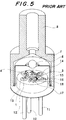
- Fig.5 is a perspective view of a prior photodiode module.
- Fig.8 is a plan view of the package.
- the package (1) is a general-use package on sale.
- a photodiode (3) and a preamplifier IC (4) are mounted on a print plate (15).
- a source (power supply) pattern (16) and a ground pattern (17) are formed on the print plate (15).
- a wire connects the source (power supply) pattern (16) with a source pin (11).
- a ring electrode on the photodiode (3) is joined to an input terminal of the preamplifier IC (4) with a wire.
- the ground pattern (17) is jointed to the package by another wire.
- a chip capacitor (18) bridges the source pattern (16) and the ground pattern (17). The ends of the capacitor are soldered on both the source pattern (16) and the ground pattern (17).
- the photodiode is fixed at the center of the upper surface of the package.
- the preamplifier (4) and the chip capacitor (18) are fixed on reverse sides with regard to the photodiode chip (3) on the package.
- the amplified signal from the preamplifier (4) is taken out from an output pin (12) of the package.
- a cap (7) with a lens(6) covers the upper surface of the package (1).
- the light-receiving region of the photodiode is aligned in a central axial line of the lens.
- the cap (7) is welded by a laser at the adjusted position of the package.
- a sleeve (8) for fitting a ferrule is positioned and welded by a laser on the package outside of the cap (7).
- a ferrule holding an end of an optical fiber is inserted and fixed in the sleeve (8).
- Fig.6 is a perspective section of another prior photodiode module.
- the module forms a special patterns (19) and (20) on the upper surface (5) of the package (1).
- the ground pattern (19) is made from a rectangular metal pattern which is connected to a case pin (10) below.
- the source pattern (20) is bow-shaped metal pattern which is connected to a source pin (11) below.
- the package (1) has a metal disc part, three pins (10), (11), (12) and an insulator (13) which maintains the pins to the disc part, and electrically separates these pins from the disc.
- the insulator (13) is denoted by dots in Fig.6.
- the insulator (13) has the role of unifying these parts and sealing the inner space of the package.
- the prior module used special pins and a single-purposed package which had been made only for this device.
- the photodiode (3) and the preamplifier (4) are mounted on the central ground pattern (19) which connects with the case pin (10).
- the bottom surface of the photodiode is a cathode of the diode. Thus, the bottom surface must electrically be isolated from the ground pattern (19) below.
- an insulating spacer (9) is stuck to the ground pattern (19).
- the photodiode chip (3) is furnished on the insulating spacer (9).
- the source pattern (20) is connected by a wire to the upper metal-coated surface of the insulating spacer. Another wire joins the source pattern (20) to an electrode pad of the preamplifier IC (4).
- Prior modules of example 1 and example 2 accomplish such a circuit designated by Fig.9.
- electrodes of a capacitor (2) or (18) are connected to the source pin (11) and to the ground pin (10).
- the source pad of the preamplifier is jointed by the wire (22) to the source pin (11).
- the ground pad of the preamplifier is connected by the wire (24) to the case pin (ground pin) (10).
- the output of the preamplifier (4) is joined to the signal output pin (12).
- the cathode of the photodiode (3) communicates with the source.
- the anode of the photodiode (3) is connected to the preamplifier IC (4).
- the source line (16) corresponds to the pattern (16) and the ground line (17) corresponds to the pattern (17).
- the source line is the source pattern (20) and the ground line is the ground pattern (19).
- a conventional photodiode module mounts a photodiode and a preamplifier close together in a package. Furthermore, a capacitor is inserted between the source voltage and the ground voltage of the photodiode and the preamplifier for stabilizing the performance of the photodiode module.
- the capacitor reduces the AC resistance of the power source and prevents the noise riding on the source line from entering the device by forming a noise filter in the source.
- the power source which is connected by the pins to the device is accompanied by a capacitor of a big capacitance. The external, big capacitance also decreases the impedance of the power source.
- a small print plate (15) on which a capacitor, a photodiode and a preamplifier are furnished together is fixed on a package (Fig.5).
- a special package having the patterns (19) and (20) on which a capacitor, a photodiode and a preamplifier are upholstered together is used (Fig.6).
- a purpose of the present invention is to provide a small-sized photodetector module. Another purpose of the present invention is to provide a photodetector module which can be produced by facile steps. Another purpose of the present invention is to provide a photodetector module which can be produced with low cost.
- bypass capacitor in a pertinent position which is used as a filter for reducing the AC resistance of the power source, eliminating the ripple of the voltage and getting rid of the noise.
- the photodetector module of the present invention is characterized by an adoption of a parallel plate capacitor which has two parallel electrodes sandwiching a dielectric medium.
- the photodiode module is produced by fitting a parallel plate capacitor at the center of a package and sticking a photodiode on the parallel plate capacitor.
- the upper surface of the parallel plate capacitor is allotted to the source pattern for the photodiode. Since the photodiode is piled on the parallel plate capacitor, the device can save the area for mounting the capacitor.
- This invention is characterized by the three-dimensional structure of heaping the photodiode on the capacitor.
- the parallel plate capacitor is a new type of capacitor which has a flat dielectric medium and two parallel electrodes which sandwich the flat dielectric medium.
- the bottom (cathode) of a photodiode should be connected to the power source, as shown in Fig.9.
- the structure of the photodiode enables the device to ride the photodiode directly on the top surface of the parallel plate capacitor which shall be the source pattern for the diode.
- This invention fixes the parallel plate capacitor on a package and mounts the photodiode on the parallel plate capacitor.
- the two-story structure of the capacitor and the photodiode features this invention.
- the two-story structure is novel.
- the structure enables the module to reduce the mounting area of the package. The reduction of the necessary area can miniaturize the module.
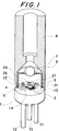
- Fig.1 is a perspective view of a vertical section of a photodiode module of a first embodiment of the present invention.
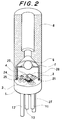
- Fig.2 is a perspective view of a vertical section of a photodiode module of a second embodiment of the present invention.
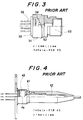
- Fig. 3 is a partially sectioned side view of the pre-Amp containing PD module disclosed by Horigome et al., 1990 Spring Conference of Electronics Information Communication Society, the 4th-volume, C271, p4-326(1990).
- Fig.4 is a partially sectioned side view of the pre-Amp containing PD module proposed by Sawai et al., 1993 Spring Conference of Electronics Information Communication Society, the 4th-volume, C186, p4-222(1993).
- Fig.5 is a perspective view of a vertical section of a prior photodiode module which is produced by mounting a capacitor, a photodiode and a preamplifier on a special print plate on which a source pattern and a ground pattern have been depicted.
- Fig.6 is a perspective view of a vertical section of another prior photodiode module which unifies a source-pattern pin, a signal output pin and a ground-pattern pin with an insulator to a package.
- Fig.7 is a plan view of the package of the embodiment of Fig.1.
- Fig.8 is a plan view of the package of the prior module of Fig.5.
- Fig.9 is a diagram of the electric circuit of the photodetector module of the first embodiment of Fig.1.
- Fig.10 is a diagram of the electric circuit of the photodiode module of the second embodiment of Fig.2.
- Fig.11 is a perspective view of a parallel plate capacitor.
- Fig.12 is perspective views of four examples of the parallel plate capacitor which is interposed between two microstrip lines.
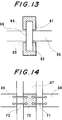
- Fig.13 is a plan view of two parallel plate capacitors interposed between two ground surfaces and a metal pattern.
- Fig.14 is a plan view of three metal patterns and a parallel plate capacitor connected to the patterns.
- Fig.15 is a graph showing the frequency performance of the photodiode module of the present invention (solid line) and the prior module (dotted line).
- Fig.16 is a sectional view of the mount of the photodiode module of the present invention which mounts a parallel plate capacitor on the package with a solder and fixes a photodiode chip on the capacitor with another solder.
- This invention bonds a parallel plate capacitor at a center of a package and fits a photodiode on the capacitor.
- the structure can be called a two-story structure briefly.
- the two-story structure saves the area for placing a capacitor and dispenses with a wire which connects the capacitor to the source pattern and another wire which couples the capacitor to the ground pattern.
- the saving of the area enables this invention to miniaturize the module.
- the reduction of the parts simplifies the steps of fabricating the module and reduces the cost of production.
- the most important matter of this invention is the use of the parallel plate capacitor.
- the use of the parallel plate capacitor allows the photodiode to ride on the capacitor.
- Other type of capacitor forbids another device from riding on it.
- the fiber, the lens, the photodiode and the capacitor align along a central line with rotational symmetry.
- Electric or electronic parts are used to be arranged in two dimensional relations either on a print circuit plate or on a package.
- capacitors with a small capacitance of pico Farads (pF) are usually made from a dielectric of oxides of titanium (Ti) or tantalum (Ta). Mica capacitors cover the capacitance region from pF to micro Farads ( ⁇ F).
- Electrolytic capacitors with a big capacitance are used for stabilizing the power source. The capacitor winds a strip having a dielectric and metal sheets sandwiching the dielectric in many turns for increasing the capacitance.
- capacitors can be sorted by the connecting parts. Most popular capacitors have two parallel pins for connecting them to external devices.
- the pin type capacitor is fixed to a print circuit plate having copper plating patterns on the bottom surface by boring holes, inserting the pins to some pertinent holes, soldering the pins to the Cu print patterns and cutting extra length of the pins.
- Chip capacitors are used in hybrid integrated circuits (IC).
- the chip capacitor is a rectangular solid having flat electrodes on both ends instead of pins.
- the chip capacitor is fixed to a print plate with Cu patterns coated with a solder of a hybrid IC by positioning the chip capacitor at a suitable spot, carrying the print plate in a reflow furnace, melting the solder and soldering the side electrodes to the Cu patterns.
- the pin type capacitors and the chip type capacitors have been used since a long time before.
- a capacitor is a device which sandwiches a dielectric film by two metal sheets in principle.
- Usual textbooks of electronics depict a schematic view of a capacitor which has a dielectric medium and two electrodes holding the dielectric between them.
- the parallel electrodes and a flat dielectric medium are a simplified concept of a capacitor.
- a parallel plate capacitor however, has not been used since long before, because such a capacitor could not be produced yet owing to the difficulty of making a very thin dielectric film without a leak current.
- Pin type capacitors or chip type capacitors are not built simply with parallel electrodes and a flat dielectric medium.
- Recent development of thin film technology enables to make a quite thin film without holes and to produce new parallel electrode capacitors in which parallel flat electrodes sandwich a flat dielectric medium.
- Dielectric Laboratories Inc. in U.S.A. produces and sales parallel plate capacitors with the trademark of "di-cap".
- the capacitor is built by sandwiching a ceramic dielectric by Au layers.
- the Au layers are electrodes.
- the reason why the electrodes are made of gold is that gold layers enable the capacitor to be directly soldered to copper patterns.
- the capacitor is a thin rectangular parallelepiped having electrodes on both surfaces.
- the capacitor can be directly ridden on a microstrip line and be soldered on the line.
- the use of the di-cap allows the microstrip line to reduce the self induction L and to prohibit the reflection of signals at the capacitor by equalizing the width of the capacitor to the width of the line.
- Low resistance metal layers are directly in contact with the dielectric layer.
- the capacitor need not use narrow wires for jointing the capacitor to an external device unlike other types of capacitors.
- the self-induction L of the connection lines is small enough.
- the capacitors are suitable for high frequency circuits which are suitable for the treatment as a distributed parameter circuit.
- the width W of the "di-cap” ranges from 0.254mm to 2.286mm.
- the length L ranges from 0.254mm to 2.540mm.
- the thickness T is from 0.102mm to 0.254mm.
- the withstanding voltage of the "di-cap” is 50V or 100V. No capacitor with other withstanding voltage has not been sold yet.
- the di-cap of a 100V withstanding voltage has a 1.5 times bigger thickness than the di-cap of a 50V withstanding voltage.
- the capacitance of the parallel plate capacitors ranges from 68pF to 1500pF.
- the DC resistance is more than 106M ⁇ .
- Fig.11 shows a parallel plate capacitor (2) which has a simple structure having a metal (50), a dielectric (51) and a metal (52) which are piled in this order.
- This capacitor is entirely different in the shape and in the mode of connection with other circuit from the pin-type capacitors or the chip capacitors.
- Fig.12 demonstrates four examples of the modes of connection in which a capacitor (2) is jointed between two metal patterns (55) and (56) which are microstrip lines.
- Mode 1 solders a parallel plate capacitor (2) at an end of a metal pattern (56) with a width equal to the width of the capacitor (2).
- the whole of the bottom surface of the capacitor (2) is joined to the pattern (56).
- the upper surface is connected by a wire (57) to an end of another pattern (55).
- Mode 2 also fits a di-cap on an end of the microstrip line (56) with a solder.
- the upper surface of the capacitor (2) is connected by two wires to another metal pattern (55). The use of two wires reduces the resistance and the self-induction of the joints.
- Mode 3 connects the upper surface of the capacitor (2) with three wires to another metal pattern (55).
- the adoption of three wires further reduces the resistance and the self-induction.
- Mode 4 couples the upper surface of the capacitor (2) to another metal pattern (55) by a wide thin metal plate (58).
- Mode 4 is the best mode of connection owing to the minimum L and R.
- Fig.13 denotes another mode of connection between the capacitors and patterns.
- a bonding stripe (66) is employed in the mode for inserting two parallel plate capacitors (61) and (62) between a microstrip line (63) and the ground patterns(64) and (65).
- the bottom surfaces of the capacitors (61) and (62) are overall stuck to the ground patterns (64) and (65).
- the upper surfaces of the capacitors (61) and (62) are connected by the bonding stripe (66) to the middle microstrip line (63).
- the whole of the bottom is entirely glued to the ground pattern.
- the upper surface is connected by the wide bonding stripe (66).
- the mode of connection can minimize the self-induction L of the connection lines.
- the examples clarify the fact that the parallel plate capacitors have wide electrodes which enables the capacitor to be soldered to metal patterns overall.
- the parallel plate capacitor is suitable for a high frequency circuit, because it can reduce the AC resistance of the connection lines.
- FIG.14 Other mode of connection is shown in Fig.14.
- This mode connects a capacitor (70) to two source patterns (68) and (69) and a ground line (67). The whole of the bottom of the capacitor (70) is soldered on the ground pattern (67).
- the upper surface is joined to a source pattern (68) by a pair of wires (71). The same surface is jointed to a different source pattern (69) by another pair of wires (72).
- Parallel plate capacitors are novel, small-seized capacitors which are preferably used between a source level and a ground level for eliminating the noise riding on the source line.
- the bottom surface is soldered to a pattern and the upper surface is connected to another pattern by wires or a stripe.
- These are the modes of mounting of parallel plate capacitors. There is no other mode of connection yet.
- This invention is novel also with regard to the connection mode of the capacitor itself in addition to the novelty of the structure of a PD module.
- Photodetector module of this invention succeeds in saving the necessary area of the package, reducing the number of parts and decreasing the steps of production by piling a photodiode on a parallel plate capacitor.
- Fig.1 is a perspective view of a vertical section of the photodiode module as an embodiment of the present invention.
- This embodiment adopts a general-use three pin package (1) of a 5.6 mm diameter.
- This is a commonplace package which has been used for a package of various kinds of transistors.
- the package has three pins (10), (11) and (12).
- One pin is a case pin (10) which is connected to the package itself.
- Another pin is a source pin (11).
- the last one is a signal output pin (12) which transmits the signal of the preamplifier to an external circuit.
- the case pin (10) is soldered to the package (1).
- Upper ends of the source pin (11) and the signal output pin (12) project over the upper surface (5) of the package (1).
- a parallel plate capacitor (2) of a capacitance of 470 pF is fixed on the package (1) with an AuSn (gold/tin) solder.
- the size of the rectangular capacitor (2) is 0.9mm ⁇ 1.0mm ⁇ 0.1mm.
- the parallel plate capacitor (2) has electrodes on the top surface and the bottom surface (0.9mm ⁇ 1.0mm). The bottom surface is glued directly with the AuSn solder to the package which is at the ground level.
- the AuSn solder has a melting point of 286°C.
- the upper surface of the parallel plate capacitor is another electrode.
- a photodiode (3) is positioned for harmonizing it with the center of the package and is fixed on the parallel plate capacitor (2) with a SnPb solder.
- the melting point of the SnPb (tin/lead) solder is 240 °C.
- the difference of the melting points of the solders is important for making the structure of Fig.1.
- the solder which glues the bottom surface of the capacitor (2) the upper face of the package (1) is called the first solder.
- the melting point of the first solder is denoted by Tc1.
- the solder which connects the bottom of the photodiode chip to the top of the capacitor (2) is called the second solder.
- the melting point is Tc2.
- the photodiode (3) is glued by the second solder to the top of the capacitor (2).
- the order of the soldering requires an inequality of Tc1>Tc2. Otherwise, when the second solder is melted, the once-solidified first solder is also melted and the parallel plate capacitor is liable to displace from the normal position.
- Tc1-Tc2 The desirable difference (Tc1-Tc2) of the melting points Tc1 and Tc2 is more than 20 °C.
- There are other probable sets of solders except the sets of AuSn and SnPb of the example.
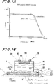
- Fig.16 exhibits the section of the mount of a parallel plate capacitor (2) and a photodiode (3) on a package.
- a parallel plate capacitor (2) is stuck on a package (1) with an AuSn solder (81). Since the parallel plate capacitor has a complete metal layer (52) on the bottom, the whole of the bottom of the capacitor (2) is soldered to the upper surface of the package (1).
- a photodiode (3) is glued with a SnPb solder (82) to the upper surface (50) of the capacitor (2).
- the bottom of the photodiode is overall a metal electrode (91) which is an n-side electrode made from gold (Au). The n-side electrode is directly soldered to the capacitor (2) with the SnPb (82).
- the bottom electrode (52) is allotted to the ground level and the top electrode (50) is assigned to the source voltage.
- a wire (21) connect's the upper surface (50) to the source pin (11).
- the photodiode (3) is produced upon an n-type substrate. Any kinds of photodiodes are available for this module.
- the substrate wafer is a crystal which can be a substrate material of a photodetector, for example, a GaAs wafer, an InP wafer or a Si wafer.
- the example of Fig.16 consists of a low resistance n-type substrate (92), a buffer layer (93), a light receiving layer (94) and a window layer (95) which are piled in this order.
- a dish-shaped p-type region (96) is formed by thermal diffusion of a p-type impurity at the center of the upper surface.
- a ring-shaped p-side electrode (97) is formed on the periphery of the p-type region (96).
- the peripheral insulator on the top is a protective layer (99) made from SiN, SiO2 etc.
- the central transparent layer is an antireflection layer (98) which is made from multilayers of two materials with different refractive indexes.
- the annular p-side electrode (97) which is an output of the photodiode (3) is connected with a wire (23) to a preamplifier.
- the preamplifier IC (4) is die-bonded at a peripheral point, as shown in Fig.1 or Fig.7. These parts are bonded on the package in the order of the parallel plate capacitor (2), the preamplifier IC (4) and the photodiode (3). After the parts have been bonded on the package, the parts, the print patterns and the pins are joined by wirebonding of gold (Au) wires of a 20 ⁇ m diameter.
- Au gold
- a metal cap (7) with a lens (6) is fitted on the package (1) in the atmosphere of dry nitrogen gas.
- the position of the cap (7) is determined at the spot which maximizes the power of the vertically incident light through the lens (6) into the photodiode (3).
- the cap (7) is welded by the resistor welding at the spot on the package (1).
- the resistor welding can be replaced by the laser welding.
- the inner space of the cap is airtightly sealed by the welding.
- a ferrule-holding sleeve (8) is positioned on the package.
- the optimum position of the sleeve (8) is determined by inserting a fiber into the sleeve, sending light in the fiber, observing the light power at the photodiode and maximizing the light power.
- the sleeve (8) is fixed at the optimum point by welding, that is, by the YAG laser welding or the resistor welding. In the example, the sleeve (8) is fixed on the package. Otherwise, the sleeve (8) can be fitted on the cap (7).
- the two-story structure of the PD and the capacitor enables this invention to mount all the necessary parts within the central area of a 3.0 mm diameter on the package (1). This fact allows the device to use a general-purposed package of a 5.6 mm diameter which is far smaller than the single-purposed packages of the prior devices (Fig.5, Fig.6 or Fig.8).
- Prior modules were used to mount a capacitor and a photodiode at different spots on a package.
- the flat structure demanded a wider area than an area of a 4.0 mm diameter for mounting the parts.
- prior modules sometimes employed a 10mm ⁇ package or an 8mm ⁇ package.
- the prior structure required at least a 7mm ⁇ package owing to the flat distribution of the parts.
- This invention succeeds in reducing the necessary area for mounting parts of the package.
- the reduction of the mounting area enables this invention to miniaturize photodiode modules.
- the two-story mount of the module dispenses with the insulating spacer of the photodiode which electrically insulates the photodiode from the package.
- the omission of the spacer alleviates the number of the parts and the steps of production.
- Frequency performance of the photodiode module which is driven by the signal rate of 125 Mbit/s is measured in order to estimate the quality of the photodiode module.
- Fig. 15 denotes the results.
- the frequency performance of the prior one is also denoted in the same graph.
- the solid line shows the result of this invention.
- the dotted line shows the property of the prior one.
- the abscissa is the frequency (MHz) of modulation.
- the ordinate is the output of the signal of the module in a unit of dB. This invention can accomplish a flat response property till more than 150 MHz.
- the 3-dB attenuation frequency is 200 MHz.
- the prior one obtains a flat response property till 90 MHz but suffers from a peaking at 100 MHz.
- the 3-dB attenuation frequency is 130 MHz. This result exhibits that the module of this invention enjoys more excellent high frequency performance than the prior one.
- the above is an embodiment which utilizes the capacitor (2) sandwiched between the package (1) and the photodiode (3) in common both as a bypass capacitor of the photodiode and as a bypass capacitor of the preamplifier. Otherwise, the capacitor can solely be allotted to the bypass capacitor either for the photodiode or the preamplifier.
- Fig.2 shows another embodiment which makes use of the capacitor as the bypass capacitor only of a photodiode.
- a four-pin package is employed in the second embodiment for separating the source line of the photodiode from the source line of the preamplifier. Then two independent source pins are prepared in the package respectively to the photodiode (3) and the preamplifier (4).
- the parallel plate capacitor (2) is made use of the bypass capacitor solely for the photodiode (3).
- Fig.2 is the perspective view of the second embodiment and Fig.10 is the circuit diagram of the same module.
- a parallel plate capacitor (2) is soldered by the AuSn solder at the center of the package (1).
- a photodiode (3) is soldered with the SnPb on the capacitor (2).
- a preamplifier IC (4) is also soldered at a periphery of the package (1).
- the bottom of the preamplifier (4) and the bottom of the capacitor (2) are at the ground level, since they are directly bonded on the case (package) which is connected to the ground pin (10).
- a PD source pin (11) is connected by a wire (21) to the upper surface of the parallel plate capacitor (2).
- the preamplifier source pin (27) is joined by a wire (28) to a source pad of the preamplifier(4).
- the source pins (11) and (27) are separated in order to supply the photodiode (3) and the preamplifier (4) with different voltages or different DC impedance.
- the isolation of the photodiode (3) from the preamplifier (4) is effective to cut the noise or to suppress the parasitic oscillation.
- An annular electrode (p-side electrode) of the photodiode (3) is coupled by a wire (23) to an input pad of the preamplifier (4).
- a signal output pad of the preamplifier (4) is joined by a wire (25) to a signal output pin (12).
- a wire (24) connects a ground pad of the preamplifier (4) to the case (package(1)).
- An increase of the pin (27) hardly enlarges the size of the package in the four-pin module.
- This invention does not restrict the photodiode to an n-type substrate one.
- a p-type substrate photodiode is also available in the module. In the case of the p-type substrate photodiode, the voltage applied from the source is negative. The polarities of parts are all reverse.
- the photodiode which has been built on a semi-insulating semiconductor is also applicable, for example, a GaAs photodiode. In this case, no current flows throughout the substrate. Thus, the upper electrode of the capacitor should be joined to the source pad of the photodiode chip.
- the module does not restrict the driving voltage to 5 V. This invention can be applied to any device of any driving voltage.
- this invention is not confined to the 5.6mm ⁇ package but can be applied to any sized package with any number of pins. This invention narrows the mounting area on any package and reduces the number of the parts.
- the parallel plate capacitor can take various sizes and various shapes in this invention.
- the wire is not restricted to gold (Au).
- Cu wires or Al wires can be also utilized to connect the electrodes and pads in the module.
- the mode of connection of wires is not restricted to the mode shown in Fig.1 or Fig.2.
- This invention succeeds in miniaturization of a photodiode module and in simplifying the steps of production of a photodiode module by piling a photodiode on a parallel plate capacitor.
- the difference of the necessary areas will easily be understood by comparing the plan views of the packages.
- Fig.7 is the plan view of the package of the present invention.
- Fig.8 is the plan view of the package of the prior module of Fig.5. The comparison verifies the excellence of the present invention.
Abstract
Description
- This invention relates to a photodetector module which is utilized in optoelectronic communication systems and a method of making the photodetector module. The photodetector module is a device which receives optical signals propagating in an optical fiber and converts the optical signals into electric signals. A photodetector module is produced by mounting a photodiode chip, a preamplifier chip and a capacitor on a package, sealing the package with a cap having a window and sticking a sleeve above the cap to the package. The sleeve is a cylindrical receptacle in which an end of an optical fiber will be inserted. A lens is often fitted on the window of the cap in order to converge the light beams emitted from the end of an optical fiber on the photodiode chip. The device is called a "photodetector" module, because the device has a photodiode which converts optical signals to electric signals and a preamplifier for amplifying the electric signals in the same package.
- This application claims a priority based on Japanese Patent Application NO. 126973/1994 filed 16 May, 1994. Prior photodetecting device was usually built of a package and a photodiode chip mounted on the package. Optical signals are converted to electric signals by the photodiode and are output from the device. The electric signals are amplified by an preamplifier which is furnished on a print circuit plate out of the photodetecting device. The outer-installed preamplifier, however, cannot prevent external noise from mixing with a weak signal, since a weak signal propagates in a long, narrow wire. In the case of a high frequency signal, the self-induction L of the long wire deforms the electric signal. Contrivance which furnishes a photodiode and a preamplifier on close positions in the same package has been suggested in order to suppress the bad influence of the external noise. For example, the following module was proposed;
- The proposed PD module has a stem (30), a plate (34) fixed on the stem (30), a photodiode and a preamplifier which are mounted together on the plate (34). A cap (31) is positioned and is welded on the stem (30) by a laser. A lens (32) has been fitted in an opening of the cap (31). A receptacle (33) is also positioned and is welded on the front end of the cap (31). The photodiode is an InGaAs-PIN photodiode. The preamplifier is a Si bipolar transistor type amplifier. The PD module adopts an optical fiber with a core of a 50 µm diameter and a cladding of a 125 µm diameter. This module has a diameter of 10 mm and a length of 14 mm. The report writes that the -3dB attenuating frequency is 200 MHz. The author describes that the device obtained a flat frequency performance without peaking and the necessary properties for an optical network of a 100 Mbit/sec band. The device has a photodiode and a preamplifier mounted on a print plate. The electrode pads and patterns are connected by bonding wires between them. The purpose of the PD module is to enhance the speed of response and reliability of the device by assembling the preamplifier in the package together with the photodiode.
- The device is produced by mounting a photodiode and a preamplifier on a plate (44) fixed on a stem (40), positioning a cap (41) having a lens and fixing the cap (41) on the stem (40). The device has a receptacle (holder) on the cap (41). An end of a fiber assembly (42) is inserted into the receptacle. A nut prevents the fiber end from being plucking out of the receptacle. The preamplifier is a Si bipolar transistor type. The photodetector is an InGaAs-PIN photodiode with a light-receiving region of an 80 µm diameter. In the case of making a device of high sensitivity, the device is built with a GaAs-FET preamplifier and an InGaAs-PIN photodiode with a light-receiving region of a 50 µm diameter. The optical fiber is a single-mode fiber with a core of a 10 µm diameter and a cladding of a 125 µm outer diameter. The module has a 7 mm diameter except for the flange and a 24 mm length.
- These improvements try to cut the noise commonly by mounting a photodiode and a preamplifier together in a package and shortening signal propagating wires. These photodiode modules use a special IC (integrated circuit) for the preamplifier of the signal of the photodiode. Fig.3 and Fig.4 do not clearly depict the way of mounting the preamplifier and the photodiode on the package. Thus, two examples will be described for clarifying the way of mounting the photodiode and the preamplifier.
- Fig.5 is a perspective view of a prior photodiode module. Fig.8 is a plan view of the package. The package (1) is a general-use package on sale. A photodiode (3) and a preamplifier IC (4) are mounted on a print plate (15). A source (power supply) pattern (16) and a ground pattern (17) are formed on the print plate (15). A wire connects the source (power supply) pattern (16) with a source pin (11). A ring electrode on the photodiode (3)is joined to an input terminal of the preamplifier IC (4) with a wire. The ground pattern (17) is jointed to the package by another wire.
- A chip capacitor (18) bridges the source pattern (16) and the ground pattern (17). The ends of the capacitor are soldered on both the source pattern (16) and the ground pattern (17). The photodiode is fixed at the center of the upper surface of the package. The preamplifier (4) and the chip capacitor (18) are fixed on reverse sides with regard to the photodiode chip (3) on the package. The amplified signal from the preamplifier (4) is taken out from an output pin (12) of the package.
- A cap (7) with a lens(6) covers the upper surface of the package (1). The light-receiving region of the photodiode is aligned in a central axial line of the lens. Then the cap (7) is welded by a laser at the adjusted position of the package. Furthermore, a sleeve (8) for fitting a ferrule is positioned and welded by a laser on the package outside of the cap (7). A ferrule holding an end of an optical fiber is inserted and fixed in the sleeve (8).
- Fig.6 is a perspective section of another prior photodiode module. The module forms a special patterns (19) and (20) on the upper surface (5) of the package (1). The ground pattern (19) is made from a rectangular metal pattern which is connected to a case pin (10) below. The source pattern (20) is bow-shaped metal pattern which is connected to a source pin (11) below. The package (1) has a metal disc part, three pins (10), (11), (12) and an insulator (13) which maintains the pins to the disc part, and electrically separates these pins from the disc. The insulator (13) is denoted by dots in Fig.6. The insulator (13) has the role of unifying these parts and sealing the inner space of the package. The prior module used special pins and a single-purposed package which had been made only for this device.
- The photodiode (3) and the preamplifier (4) are mounted on the central ground pattern (19) which connects with the case pin (10). The bottom surface of the photodiode is a cathode of the diode. Thus, the bottom surface must electrically be isolated from the ground pattern (19) below. For the purpose of isolating the photodiode chip, an insulating spacer (9) is stuck to the ground pattern (19). The photodiode chip (3) is furnished on the insulating spacer (9). The source pattern (20) is connected by a wire to the upper metal-coated surface of the insulating spacer. Another wire joins the source pattern (20) to an electrode pad of the preamplifier IC (4).
- Prior modules of example 1 and example 2 accomplish such a circuit designated by Fig.9. In the circuit, electrodes of a capacitor (2) or (18) are connected to the source pin (11) and to the ground pin (10). The source pad of the preamplifier is jointed by the wire (22) to the source pin (11). The ground pad of the preamplifier is connected by the wire (24) to the case pin (ground pin) (10). The output of the preamplifier (4) is joined to the signal output pin (12). The cathode of the photodiode (3) communicates with the source. The anode of the photodiode (3) is connected to the preamplifier IC (4).
- In the module of Fig.5 and Fig.8, the source line (16) corresponds to the pattern (16) and the ground line (17) corresponds to the pattern (17). In the module of Fig.6, the source line is the source pattern (20) and the ground line is the ground pattern (19).
- A conventional photodiode module mounts a photodiode and a preamplifier close together in a package. Furthermore, a capacitor is inserted between the source voltage and the ground voltage of the photodiode and the preamplifier for stabilizing the performance of the photodiode module. The capacitor reduces the AC resistance of the power source and prevents the noise riding on the source line from entering the device by forming a noise filter in the source. Of course, the power source which is connected by the pins to the device is accompanied by a capacitor of a big capacitance. The external, big capacitance also decreases the impedance of the power source. An AC resistance, however, arises in the source line due to the self-induction L of the pins and the wires, which raises the impedance substantially. Prevention of the rise of the AC impedance requires an insertion of another capacitor at a point quite close to the preamplifier and the photodiode. Prior modules have installed a capacitor in the package for the reason. The capacitor plays the role of the filter of abating the AC resistance of the source line, eliminating the ripple of the voltage and removing the noise. Conventional photodiode modules have the following structures as mentioned till now;
- A small print plate (15) on which a capacitor, a photodiode and a preamplifier are furnished together is fixed on a package (Fig.5).
- A special package having the patterns (19) and (20) on which a capacitor, a photodiode and a preamplifier are upholstered together is used (Fig.6).
- These prior structures still suffer from some difficulties. The additional use of a print plate complicates the steps of mounting parts on the package in
structure ①. The use of the special package having complex patterns (19) and (20) raises the cost of production. Besides, the horizontal disposition of the capacitor and the photodiode demands a wide area for mounting, which enlarges the package. In particular, the capacitor has a broader size than the photodiode or the amplifier in general. Bothstructures - A purpose of the present invention is to provide a small-sized photodetector module. Another purpose of the present invention is to provide a photodetector module which can be produced by facile steps. Another purpose of the present invention is to provide a photodetector module which can be produced with low cost.
- These difficulties can be eliminated by disposing the bypass capacitor in a pertinent position which is used as a filter for reducing the AC resistance of the power source, eliminating the ripple of the voltage and getting rid of the noise.
- The photodetector module of the present invention is characterized by an adoption of a parallel plate capacitor which has two parallel electrodes sandwiching a dielectric medium. The photodiode module is produced by fitting a parallel plate capacitor at the center of a package and sticking a photodiode on the parallel plate capacitor. The upper surface of the parallel plate capacitor is allotted to the source pattern for the photodiode. Since the photodiode is piled on the parallel plate capacitor, the device can save the area for mounting the capacitor. This invention is characterized by the three-dimensional structure of heaping the photodiode on the capacitor. The parallel plate capacitor is a new type of capacitor which has a flat dielectric medium and two parallel electrodes which sandwich the flat dielectric medium. Inherently the bottom (cathode) of a photodiode should be connected to the power source, as shown in Fig.9. The structure of the photodiode enables the device to ride the photodiode directly on the top surface of the parallel plate capacitor which shall be the source pattern for the diode.
- This invention fixes the parallel plate capacitor on a package and mounts the photodiode on the parallel plate capacitor. The two-story structure of the capacitor and the photodiode features this invention. The two-story structure is novel. The structure enables the module to reduce the mounting area of the package. The reduction of the necessary area can miniaturize the module. The elimination of the special-purposed plate of Fig.5 and the spacer of Fig.6 simplifies the steps of production. This invention can realize a small, inexpensive and high-performance photodetector module.
- The invention will be more fully understood from the following description given by way of example only with reference to the several figures of the accompanying drawings in which,
- Fig.1 is a perspective view of a vertical section of a photodiode module of a first embodiment of the present invention.
- Fig.2 is a perspective view of a vertical section of a photodiode module of a second embodiment of the present invention.
- Fig. 3 is a partially sectioned side view of the pre-Amp containing PD module disclosed by Horigome et al., 1990 Spring Conference of Electronics Information Communication Society, the 4th-volume, C271, p4-326(1990).
- Fig.4 is a partially sectioned side view of the pre-Amp containing PD module proposed by Sawai et al., 1993 Spring Conference of Electronics Information Communication Society, the 4th-volume, C186, p4-222(1993).
- Fig.5 is a perspective view of a vertical section of a prior photodiode module which is produced by mounting a capacitor, a photodiode and a preamplifier on a special print plate on which a source pattern and a ground pattern have been depicted.
- Fig.6 is a perspective view of a vertical section of another prior photodiode module which unifies a source-pattern pin, a signal output pin and a ground-pattern pin with an insulator to a package.
- Fig.7 is a plan view of the package of the embodiment of Fig.1.
- Fig.8 is a plan view of the package of the prior module of Fig.5.
- Fig.9 is a diagram of the electric circuit of the photodetector module of the first embodiment of Fig.1.
- Fig.10 is a diagram of the electric circuit of the photodiode module of the second embodiment of Fig.2.
- Fig.11 is a perspective view of a parallel plate capacitor.
- Fig.12 is perspective views of four examples of the parallel plate capacitor which is interposed between two microstrip lines.
- Fig.13 is a plan view of two parallel plate capacitors interposed between two ground surfaces and a metal pattern.
- Fig.14 is a plan view of three metal patterns and a parallel plate capacitor connected to the patterns.
- Fig.15 is a graph showing the frequency performance of the photodiode module of the present invention (solid line) and the prior module (dotted line).
- Fig.16 is a sectional view of the mount of the photodiode module of the present invention which mounts a parallel plate capacitor on the package with a solder and fixes a photodiode chip on the capacitor with another solder.
- To achieve the foregoing objects and in accordance with the purpose of the invention, embodiments will be broadly described herein;
- This invention bonds a parallel plate capacitor at a center of a package and fits a photodiode on the capacitor. The structure can be called a two-story structure briefly. The two-story structure saves the area for placing a capacitor and dispenses with a wire which connects the capacitor to the source pattern and another wire which couples the capacitor to the ground pattern. The saving of the area enables this invention to miniaturize the module. The reduction of the parts simplifies the steps of fabricating the module and reduces the cost of production.
- The most important matter of this invention is the use of the parallel plate capacitor. The use of the parallel plate capacitor allows the photodiode to ride on the capacitor. Other type of capacitor forbids another device from riding on it. Thus the fiber, the lens, the photodiode and the capacitor align along a central line with rotational symmetry. Nobody has tried to mount an electric part on another electric part as yet. It contradicts the common sense of the skilled to pile a part upon another part. Electric or electronic parts are used to be arranged in two dimensional relations either on a print circuit plate or on a package.
- What enables this invention to dispose the parts in three dimensional relation is the parallel plate capacitor which is a novel type of capacitor.
- Therefore, it may be desirable to explain the parallel plate capacitor at first. Many different kinds (paper capacitor, film capacitor, electrolytic capacitor, mica capacitor, ceramic capacitor etc.) of capacitors have been produced and used in accordance with the differences of the capacitance or the withstanding voltage. Capacitors with a small capacitance of pico Farads (pF) are usually made from a dielectric of oxides of titanium (Ti) or tantalum (Ta). Mica capacitors cover the capacitance region from pF to micro Farads (µ F). Electrolytic capacitors with a big capacitance are used for stabilizing the power source. The capacitor winds a strip having a dielectric and metal sheets sandwiching the dielectric in many turns for increasing the capacitance.
- In addition to the classification by the withstanding voltage and the capacitance, capacitors can be sorted by the connecting parts. Most popular capacitors have two parallel pins for connecting them to external devices. The pin type capacitor is fixed to a print circuit plate having copper plating patterns on the bottom surface by boring holes, inserting the pins to some pertinent holes, soldering the pins to the Cu print patterns and cutting extra length of the pins. Chip capacitors are used in hybrid integrated circuits (IC). The chip capacitor is a rectangular solid having flat electrodes on both ends instead of pins. The chip capacitor is fixed to a print plate with Cu patterns coated with a solder of a hybrid IC by positioning the chip capacitor at a suitable spot, carrying the print plate in a reflow furnace, melting the solder and soldering the side electrodes to the Cu patterns. The pin type capacitors and the chip type capacitors have been used since a long time before.
- A capacitor is a device which sandwiches a dielectric film by two metal sheets in principle. Usual textbooks of electronics depict a schematic view of a capacitor which has a dielectric medium and two electrodes holding the dielectric between them. The simplified figures used to show two parallel electrodes and a flat dielectric medium maintained therebetween. The parallel electrodes and a flat dielectric medium are a simplified concept of a capacitor. A parallel plate capacitor, however, has not been used since long before, because such a capacitor could not be produced yet owing to the difficulty of making a very thin dielectric film without a leak current. The capacitance C is in proportion to the area S of the dielectric and the dielectric constant ε, but in reverse proportion to the thickness d of the dielectric. Namely, C = εS/d. Prior capacitors used to wind or fold a sheet of a dielectric sandwiched by conductors and insulators in many turns in order to raise the total capacitance by enhancing the effective area S of the dielectric medium. Pin type capacitors or chip type capacitors are not built simply with parallel electrodes and a flat dielectric medium.
- Recent development of thin film technology enables to make a quite thin film without holes and to produce new parallel electrode capacitors in which parallel flat electrodes sandwich a flat dielectric medium.
- For example, Dielectric Laboratories Inc., in U.S.A. produces and sales parallel plate capacitors with the trademark of "di-cap". The capacitor is built by sandwiching a ceramic dielectric by Au layers. The Au layers are electrodes. The reason why the electrodes are made of gold is that gold layers enable the capacitor to be directly soldered to copper patterns. The capacitor is a thin rectangular parallelepiped having electrodes on both surfaces. Thus, the capacitor can be directly ridden on a microstrip line and be soldered on the line. The use of the di-cap allows the microstrip line to reduce the self induction L and to prohibit the reflection of signals at the capacitor by equalizing the width of the capacitor to the width of the line.
- Low resistance metal layers are directly in contact with the dielectric layer. The capacitor need not use narrow wires for jointing the capacitor to an external device unlike other types of capacitors. The self-induction L of the connection lines is small enough. Thus the capacitors are suitable for high frequency circuits which are suitable for the treatment as a distributed parameter circuit.
- The width W of the "di-cap" ranges from 0.254mm to 2.286mm. The length L ranges from 0.254mm to 2.540mm. The thickness T is from 0.102mm to 0.254mm. The withstanding voltage of the "di-cap"is 50V or 100V. No capacitor with other withstanding voltage has not been sold yet. The di-cap of a 100V withstanding voltage has a 1.5 times bigger thickness than the di-cap of a 50V withstanding voltage. The capacitance of the parallel plate capacitors ranges from 68pF to 1500pF. The DC resistance is more than 106MΩ.
- For example, a di-cap of 68pF with a 50V withstanding voltage has a width W = 0.254mm, a length L = 0.254mm and a thickness T = 0.102mm. Another di-cap of 470pF with a 50V withstanding voltage has W = 0.635mm, L = 0.762mm and T = 0.102mm. Since the thickness of the dielectric is restricted within a narrow scope, the size differs according to the difference of the capacitance. The area WL is in proportion to the capacitance C.
- Fig.11 shows a parallel plate capacitor (2) which has a simple structure having a metal (50), a dielectric (51) and a metal (52) which are piled in this order. This capacitor is entirely different in the shape and in the mode of connection with other circuit from the pin-type capacitors or the chip capacitors.
- Fig.12 demonstrates four examples of the modes of connection in which a capacitor (2) is jointed between two metal patterns (55) and (56) which are microstrip lines.
-
Mode ① solders a parallel plate capacitor (2) at an end of a metal pattern (56) with a width equal to the width of the capacitor (2). The whole of the bottom surface of the capacitor (2) is joined to the pattern (56). The upper surface is connected by a wire (57) to an end of another pattern (55). -
Mode ② also fits a di-cap on an end of the microstrip line (56) with a solder. The upper surface of the capacitor (2) is connected by two wires to another metal pattern (55). The use of two wires reduces the resistance and the self-induction of the joints. -
Mode ③ connects the upper surface of the capacitor (2) with three wires to another metal pattern (55). The adoption of three wires further reduces the resistance and the self-induction. -
Mode ④ couples the upper surface of the capacitor (2) to another metal pattern (55) by a wide thin metal plate (58). - The use of plural wires prevents the delay, the deformation and the reflection of signals by decreasing the AC resistance R and the induction L of the line.
Mode ④ is the best mode of connection owing to the minimum L and R. - Fig.13 denotes another mode of connection between the capacitors and patterns. A bonding stripe (66) is employed in the mode for inserting two parallel plate capacitors (61) and (62) between a microstrip line (63) and the ground patterns(64) and (65). The bottom surfaces of the capacitors (61) and (62) are overall stuck to the ground patterns (64) and (65). The upper surfaces of the capacitors (61) and (62) are connected by the bonding stripe (66) to the middle microstrip line (63). The whole of the bottom is entirely glued to the ground pattern. The upper surface is connected by the wide bonding stripe (66). The mode of connection can minimize the self-induction L of the connection lines.
- The examples clarify the fact that the parallel plate capacitors have wide electrodes which enables the capacitor to be soldered to metal patterns overall. The parallel plate capacitor is suitable for a high frequency circuit, because it can reduce the AC resistance of the connection lines.
- Other mode of connection is shown in Fig.14. This mode connects a capacitor (70) to two source patterns (68) and (69) and a ground line (67). The whole of the bottom of the capacitor (70) is soldered on the ground pattern (67). The upper surface is joined to a source pattern (68) by a pair of wires (71). The same surface is jointed to a different source pattern (69) by another pair of wires (72).
- Parallel plate capacitors are novel, small-seized capacitors which are preferably used between a source level and a ground level for eliminating the noise riding on the source line. In any cases, the bottom surface is soldered to a pattern and the upper surface is connected to another pattern by wires or a stripe. These are the modes of mounting of parallel plate capacitors. There is no other mode of connection yet. Nobody has tried another mode of mounting than the modes of Fig.12, Fig.13 and Fig.14. Thus, nobody has found a mode of placing another device on the capacitor like this invention. This invention is novel also with regard to the connection mode of the capacitor itself in addition to the novelty of the structure of a PD module.
- Then this invention is explained more in detail by preferred embodiments.
- Photodetector module of this invention succeeds in saving the necessary area of the package, reducing the number of parts and decreasing the steps of production by piling a photodiode on a parallel plate capacitor.
- An embodiment will be explained by referring to figures. Fig.1 is a perspective view of a vertical section of the photodiode module as an embodiment of the present invention. This embodiment adopts a general-use three pin package (1) of a 5.6 mm diameter. This is a commonplace package which has been used for a package of various kinds of transistors.
- The package has three pins (10), (11) and (12). One pin is a case pin (10) which is connected to the package itself. Another pin is a source pin (11). The last one is a signal output pin (12) which transmits the signal of the preamplifier to an external circuit. The case pin (10) is soldered to the package (1). Upper ends of the source pin (11) and the signal output pin (12) project over the upper surface (5) of the package (1). There are insulators (13) and (14) among the package (1), the source pin (11) and the signal output pin (12). The insulators mechanically hold the pins (11) and (12) to the package (1), separating electrically the pins from the package (1).
- A parallel plate capacitor (2) of a capacitance of 470 pF is fixed on the package (1) with an AuSn (gold/tin) solder. The size of the rectangular capacitor (2) is 0.9mm×1.0mm×0.1mm. The parallel plate capacitor (2) has electrodes on the top surface and the bottom surface (0.9mm×1.0mm). The bottom surface is glued directly with the AuSn solder to the package which is at the ground level. The AuSn solder has a melting point of 286°C. The upper surface of the parallel plate capacitor is another electrode.
- A photodiode (3) is positioned for harmonizing it with the center of the package and is fixed on the parallel plate capacitor (2) with a SnPb solder. The melting point of the SnPb (tin/lead) solder is 240 °C. The difference of the melting points of the solders is important for making the structure of Fig.1. The solder which glues the bottom surface of the capacitor (2) the upper face of the package (1) is called the first solder. The melting point of the first solder is denoted by Tc1. The solder which connects the bottom of the photodiode chip to the top of the capacitor (2) is called the second solder. The melting point is Tc2.
- After the capacitor (2) has been stuck by the first solder to the package (1), the photodiode (3) is glued by the second solder to the top of the capacitor (2). The order of the soldering requires an inequality of Tc1>Tc2. Otherwise, when the second solder is melted, the once-solidified first solder is also melted and the parallel plate capacitor is liable to displace from the normal position.
- The desirable difference (Tc1-Tc2) of the melting points Tc1 and Tc2 is more than 20 °C. The above example satisfies the condition, because Tc1 = 286°C, Tc2 = 240°C, and Tc1-Tc2 = 46°C. There are other probable sets of solders except the sets of AuSn and SnPb of the example.
- Fig.16 exhibits the section of the mount of a parallel plate capacitor (2) and a photodiode (3) on a package. A parallel plate capacitor (2) is stuck on a package (1) with an AuSn solder (81). Since the parallel plate capacitor has a complete metal layer (52) on the bottom, the whole of the bottom of the capacitor (2) is soldered to the upper surface of the package (1). A photodiode (3) is glued with a SnPb solder (82) to the upper surface (50) of the capacitor (2). The bottom of the photodiode is overall a metal electrode (91) which is an n-side electrode made from gold (Au). The n-side electrode is directly soldered to the capacitor (2) with the SnPb (82).
- The bottom electrode (52) is allotted to the ground level and the top electrode (50) is assigned to the source voltage. A wire (21) connect's the upper surface (50) to the source pin (11).
- The photodiode (3) is produced upon an n-type substrate. Any kinds of photodiodes are available for this module. The substrate wafer is a crystal which can be a substrate material of a photodetector, for example, a GaAs wafer, an InP wafer or a Si wafer. The example of Fig.16 consists of a low resistance n-type substrate (92), a buffer layer (93), a light receiving layer (94) and a window layer (95) which are piled in this order. A dish-shaped p-type region (96) is formed by thermal diffusion of a p-type impurity at the center of the upper surface. A ring-shaped p-side electrode (97) is formed on the periphery of the p-type region (96). The peripheral insulator on the top is a protective layer (99) made from SiN, SiO₂ etc. The central transparent layer is an antireflection layer (98) which is made from multilayers of two materials with different refractive indexes. The annular p-side electrode (97) which is an output of the photodiode (3) is connected with a wire (23) to a preamplifier.
- The preamplifier IC (4) is die-bonded at a peripheral point, as shown in Fig.1 or Fig.7. These parts are bonded on the package in the order of the parallel plate capacitor (2), the preamplifier IC (4) and the photodiode (3). After the parts have been bonded on the package, the parts, the print patterns and the pins are joined by wirebonding of gold (Au) wires of a 20 µm diameter.
- As clearly demonstrated in Fig.7, five wires (21) to (25) connect five
sets ① to ⑤ of pads or pins; - ① the source pin (11) and the upper surface of the capacitor (2) by a wire (21),
- ② the upper surface of the capacitor (2) and the source pad of the preamplifier IC (4) by a wire (22),
- ③ the signal output pad (anode) of the photodiode (3) and the input pad of the preamplifier (4) by a wire (23),
- ④ the output pad of the preamplifier IC (4) and the signal output pin (12) of the package (1) by a wire (25), and
- ⑤ the ground pad of the preamplifier (4) and the package (1) by a wire (24).
- A metal cap (7) with a lens (6) is fitted on the package (1) in the atmosphere of dry nitrogen gas. The position of the cap (7) is determined at the spot which maximizes the power of the vertically incident light through the lens (6) into the photodiode (3). Then the cap (7) is welded by the resistor welding at the spot on the package (1). The resistor welding can be replaced by the laser welding. The inner space of the cap is airtightly sealed by the welding.
- Then a ferrule-holding sleeve (8) is positioned on the package. The optimum position of the sleeve (8) is determined by inserting a fiber into the sleeve, sending light in the fiber, observing the light power at the photodiode and maximizing the light power. The sleeve (8) is fixed at the optimum point by welding, that is, by the YAG laser welding or the resistor welding. In the example, the sleeve (8) is fixed on the package. Otherwise, the sleeve (8) can be fitted on the cap (7).
- The two-story structure of the PD and the capacitor enables this invention to mount all the necessary parts within the central area of a 3.0 mm diameter on the package (1). This fact allows the device to use a general-purposed package of a 5.6 mm diameter which is far smaller than the single-purposed packages of the prior devices (Fig.5, Fig.6 or Fig.8).
- Prior modules were used to mount a capacitor and a photodiode at different spots on a package. The flat structure demanded a wider area than an area of a 4.0 mm diameter for mounting the parts. Thus, prior modules sometimes employed a 10mm φ package or an 8mmφ package. The prior structure required at least a 7mmφ package owing to the flat distribution of the parts.
- This invention succeeds in reducing the necessary area for mounting parts of the package. The reduction of the mounting area enables this invention to miniaturize photodiode modules. The two-story mount of the module dispenses with the insulating spacer of the photodiode which electrically insulates the photodiode from the package. The omission of the spacer alleviates the number of the parts and the steps of production.
- Frequency performance of the photodiode module which is driven by the signal rate of 125 Mbit/s is measured in order to estimate the quality of the photodiode module. Fig. 15 denotes the results. The frequency performance of the prior one is also denoted in the same graph. The solid line shows the result of this invention. The dotted line shows the property of the prior one. The abscissa is the frequency (MHz) of modulation. The ordinate is the output of the signal of the module in a unit of dB. This invention can accomplish a flat response property till more than 150 MHz. The 3-dB attenuation frequency is 200 MHz.
- The prior one obtains a flat response property till 90 MHz but suffers from a peaking at 100 MHz. The 3-dB attenuation frequency is 130 MHz. This result exhibits that the module of this invention enjoys more excellent high frequency performance than the prior one.
- The above is an embodiment which utilizes the capacitor (2) sandwiched between the package (1) and the photodiode (3) in common both as a bypass capacitor of the photodiode and as a bypass capacitor of the preamplifier. Otherwise, the capacitor can solely be allotted to the bypass capacitor either for the photodiode or the preamplifier.
- Fig.2 shows another embodiment which makes use of the capacitor as the bypass capacitor only of a photodiode. Instead of the three-pin package, a four-pin package is employed in the second embodiment for separating the source line of the photodiode from the source line of the preamplifier. Then two independent source pins are prepared in the package respectively to the photodiode (3) and the preamplifier (4). In this case, the parallel plate capacitor (2) is made use of the bypass capacitor solely for the photodiode (3). Fig.2 is the perspective view of the second embodiment and Fig.10 is the circuit diagram of the same module.
- In Fig.2, a parallel plate capacitor (2) is soldered by the AuSn solder at the center of the package (1). A photodiode (3) is soldered with the SnPb on the capacitor (2). A preamplifier IC (4) is also soldered at a periphery of the package (1). The bottom of the preamplifier (4) and the bottom of the capacitor (2) are at the ground level, since they are directly bonded on the case (package) which is connected to the ground pin (10). A PD source pin (11) is connected by a wire (21) to the upper surface of the parallel plate capacitor (2). The preamplifier source pin (27) is joined by a wire (28) to a source pad of the preamplifier(4). The source pins (11) and (27) are separated in order to supply the photodiode (3) and the preamplifier (4) with different voltages or different DC impedance. The isolation of the photodiode (3) from the preamplifier (4) is effective to cut the noise or to suppress the parasitic oscillation. These are different points from the former embodiment.
- The rest are the same as the first embodiment. An annular electrode (p-side electrode) of the photodiode (3) is coupled by a wire (23) to an input pad of the preamplifier (4). A signal output pad of the preamplifier (4) is joined by a wire (25) to a signal output pin (12). A wire (24) connects a ground pad of the preamplifier (4) to the case (package(1)). An increase of the pin (27) hardly enlarges the size of the package in the four-pin module.
- This invention does not restrict the photodiode to an n-type substrate one. A p-type substrate photodiode is also available in the module. In the case of the p-type substrate photodiode, the voltage applied from the source is negative. The polarities of parts are all reverse. The photodiode which has been built on a semi-insulating semiconductor is also applicable, for example, a GaAs photodiode. In this case, no current flows throughout the substrate. Thus, the upper electrode of the capacitor should be joined to the source pad of the photodiode chip. The module does not restrict the driving voltage to 5 V. This invention can be applied to any device of any driving voltage.
- Furthermore, this invention is not confined to the 5.6mmφ package but can be applied to any sized package with any number of pins. This invention narrows the mounting area on any package and reduces the number of the parts.
- The parallel plate capacitor can take various sizes and various shapes in this invention. The wire is not restricted to gold (Au). Cu wires or Al wires can be also utilized to connect the electrodes and pads in the module. The mode of connection of wires is not restricted to the mode shown in Fig.1 or Fig.2.
- This invention succeeds in miniaturization of a photodiode module and in simplifying the steps of production of a photodiode module by piling a photodiode on a parallel plate capacitor. The difference of the necessary areas will easily be understood by comparing the plan views of the packages. Fig.7 is the plan view of the package of the present invention. Fig.8 is the plan view of the package of the prior module of Fig.5. The comparison verifies the excellence of the present invention.
Claims (6)
- A photodetector module comprising:
a package having one or more connector pins;
a parallel plate capacitor mounted generally centrally of the package;
a photodiode mounted on the parallel plate capacitor for receiving optical signals and converting optical signals to electric signals;
a preamplifier disposed at a peripheral point on the package for amplifying the electric signals from the photodiode;
a cap with a lens sealing the upper surface of the package;
a sleeve mounted on the package or on the cap for holding a ferule at an end of an optical fiber, and;
means which connect electrically the electrode of the capacitor, the pads of the preamplifier, the electrode of the photodiode, the surface of the package and the pins of the package. - A photodetector module as claimed in claim 1, wherein the package has a case pin, a signal output pin, and a source pin.
- A module according to claim 2, wherein the package includes a photodiode source pin and a preamplifier source pin.
- A method of producing a photodetector module comprising the steps of:
soldering a parallel plate capacitor by a first solder to a central part of a package having a case pin, a source pin and a signal output pin;
securing a preamplifier at a peripheral point on the package, soldering a photodiode on the capacitor by a second solder having a lower melting point than the first solder;
wire-bonding the pads of the photodiode, the pads of the preamplifier, and the electrode of the capacitor;
positioning a cap with a lens;
fixing the cap on the package;
positioning a sleeve for holding a ferrule at an end of an optical fiber, and;
fixing the sleeve on the package or on the cap. - A method as claimed in claim 4, wherein the difference between the melting point Tc1 of the first solder and the melting point Tc2 of the second solder is greater than 20°C.
- A method as claimed in claim 5, wherein the first solder is AuSn and the second solder is SnPb.
Applications Claiming Priority (3)
| Application Number | Priority Date | Filing Date | Title |
|---|---|---|---|
| JP6126973A JP3047735B2 (en) | 1994-05-16 | 1994-05-16 | Optical receiving module and method of manufacturing the same |
| JP126973/94 | 1994-05-16 | ||
| JP12697394 | 1994-05-16 |
Publications (3)
| Publication Number | Publication Date |
|---|---|
| EP0684651A2 true EP0684651A2 (en) | 1995-11-29 |
| EP0684651A3 EP0684651A3 (en) | 1997-04-02 |
| EP0684651B1 EP0684651B1 (en) | 2001-01-17 |
Family
ID=14948485
Family Applications (1)
| Application Number | Title | Priority Date | Filing Date |
|---|---|---|---|
| EP19950302974 Expired - Lifetime EP0684651B1 (en) | 1994-05-16 | 1995-05-02 | Photodetector module and method of making same |
Country Status (7)
| Country | Link |
|---|---|
| US (1) | US5610395A (en) |
| EP (1) | EP0684651B1 (en) |
| JP (1) | JP3047735B2 (en) |
| KR (1) | KR0167628B1 (en) |
| CA (1) | CA2148894C (en) |
| DE (1) | DE69519894T2 (en) |
| TW (1) | TW275169B (en) |
Cited By (7)
| Publication number | Priority date | Publication date | Assignee | Title |
|---|---|---|---|---|
| EP0825653A2 (en) * | 1996-07-31 | 1998-02-25 | Sumitomo Electric Industries, Limited | Optoelectronic device package |
| DE19923417A1 (en) * | 1999-05-21 | 2000-11-30 | Tyco Electronics Logistics Ag | Diode holder has diode housing with attachment/positioning element(s) that makes aligned engagement between diode housing, optical plug connector in combination with latching device(s) |
| WO2003027743A1 (en) * | 2001-09-14 | 2003-04-03 | Infineon Technologies Ag | Transmitter and/or receiver arrangement for optical signal transmission |
| EP1310813A1 (en) * | 2001-11-08 | 2003-05-14 | DaimlerChrysler AG | Plug and socket for an opto-electronical plug system |
| EP1826927A1 (en) * | 2006-01-27 | 2007-08-29 | OpNext Japan, Inc. | Optical receiver module |
| EP1989796A2 (en) * | 2006-02-17 | 2008-11-12 | Finisar Corporation | Discrete bootstrapping in an optical receiver to prevent signal feedback |
| EP2003689A1 (en) * | 2007-06-15 | 2008-12-17 | Schott AG | Header, especially for electronic packages |
Families Citing this family (31)
| Publication number | Priority date | Publication date | Assignee | Title |
|---|---|---|---|---|
| JP3830583B2 (en) * | 1996-08-15 | 2006-10-04 | 富士通株式会社 | Optical semiconductor assembly |
| US5870517A (en) * | 1997-10-07 | 1999-02-09 | Integrated Device Technology, Inc. | Package including self-aligned laser diode and method of aligning a laser diode |
| US5977567A (en) | 1998-01-06 | 1999-11-02 | Lightlogic, Inc. | Optoelectronic assembly and method of making the same |
| US6585427B2 (en) | 1999-01-11 | 2003-07-01 | Intel Corporation | Flexure coupled to a substrate for maintaining the optical fibers in alignment |
| US6511236B1 (en) | 1999-09-07 | 2003-01-28 | Intel Corporation | Optoelectronic assembly and method for fabricating the same |
| US6207950B1 (en) | 1999-01-11 | 2001-03-27 | Lightlogic, Inc. | Optical electronic assembly having a flexure for maintaining alignment between optical elements |
| US6252726B1 (en) | 1999-09-02 | 2001-06-26 | Lightlogic, Inc. | Dual-enclosure optoelectronic packages |
| US6540412B2 (en) * | 2000-02-10 | 2003-04-01 | Sumitomo Electric Industries, Ltd. | Optical transceiver |
| JP4187376B2 (en) * | 2000-02-16 | 2008-11-26 | ローム株式会社 | Photoreceiver / amplifier |
| TW502492B (en) * | 2000-05-30 | 2002-09-11 | Alps Electric Co Ltd | Electronic circuit unit |
| DE10064599A1 (en) * | 2000-12-18 | 2002-07-04 | Infineon Technologies Ag | Sender receiver for bidirectional optical news and signal transmission has blocking filter to clearly separate send and receive signals |
| JP3996780B2 (en) * | 2001-03-21 | 2007-10-24 | シャープ株式会社 | Semiconductor laser device and manufacturing method thereof |
| DE10120692B4 (en) * | 2001-04-27 | 2004-02-12 | Siemens Ag | Mounting arrangement of electrical and / or electronic components on a circuit board |
| JP2002329873A (en) * | 2001-05-01 | 2002-11-15 | Mitsubishi Electric Corp | Semiconductor module and semiconductor device |
| JP2003163403A (en) * | 2001-11-29 | 2003-06-06 | Mitsubishi Electric Corp | Optical element module |
| JP2004088046A (en) | 2002-06-25 | 2004-03-18 | Sumitomo Electric Ind Ltd | Optical receiver and method of manufacturing the same |
| US7224910B2 (en) * | 2002-10-25 | 2007-05-29 | Gennum Corporation | Direct attach optical receiver module and method of testing |
| TWI247144B (en) * | 2003-12-05 | 2006-01-11 | Ind Tech Res Inst | Receiving optical subassembly |
| US7847301B2 (en) * | 2004-12-08 | 2010-12-07 | Agilent Technologies, Inc. | Electronic microcircuit having internal light enhancement |
| US20060133742A1 (en) * | 2004-12-17 | 2006-06-22 | Ruegg Eugen H | Universal multi-port optical block assembly with configurable optical port |
| JP2006253676A (en) * | 2005-03-08 | 2006-09-21 | Sumitomo Electric Ind Ltd | Optical assembly |
| JP4815869B2 (en) * | 2005-05-11 | 2011-11-16 | 住友電気工業株式会社 | Optical receiver module |
| JP2007123738A (en) * | 2005-10-31 | 2007-05-17 | Sony Corp | Optical transmission module, optical transmission/reception module and optical communication apparatus |
| JP2010034287A (en) * | 2008-07-29 | 2010-02-12 | Sumitomo Electric Ind Ltd | Cap, and optical module |
| JP5077158B2 (en) | 2008-09-09 | 2012-11-21 | 三菱電機株式会社 | Light receiving element |
| CN111865429B (en) * | 2019-04-30 | 2022-05-27 | 深圳市聚飞光电股份有限公司 | Photoelectric receiver and manufacturing method thereof |
| CN111865430A (en) * | 2019-04-30 | 2020-10-30 | 深圳市聚飞光电股份有限公司 | Photoelectric receiver |
| JP7279888B2 (en) | 2019-09-27 | 2023-05-23 | 住友電工デバイス・イノベーション株式会社 | Optical semiconductor device and method for manufacturing optical semiconductor device |
| GB2575204B (en) * | 2019-10-08 | 2020-08-19 | Hilight Semiconductor Ltd | Opto-electronic assembly |
| GB2575205B (en) | 2019-10-08 | 2020-09-09 | Hilight Semiconductor Ltd | Opto-electronic assembly |
| WO2023063196A1 (en) * | 2021-10-11 | 2023-04-20 | 古河電気工業株式会社 | Optical apparatus |
Citations (2)
| Publication number | Priority date | Publication date | Assignee | Title |
|---|---|---|---|---|
| US4707067A (en) * | 1984-02-22 | 1987-11-17 | Siemens Aktiengesellschaft | Opto-electronic module housing |
| EP0447201A2 (en) * | 1990-03-13 | 1991-09-18 | Nec Corporation | Photoelectric converter module |
Family Cites Families (6)
| Publication number | Priority date | Publication date | Assignee | Title |
|---|---|---|---|---|
| US4103157A (en) * | 1977-02-04 | 1978-07-25 | Mcdonnell Douglas Corporation | High speed photodetector and system |
| US4758767A (en) * | 1987-05-15 | 1988-07-19 | Multipoint Control Systems, Incorporated | Self-contained analog photodiode light sensing head |
| JPS63316812A (en) * | 1987-06-19 | 1988-12-26 | Toshiba Corp | Photosemiconductor device |
| JPH03238877A (en) * | 1990-02-15 | 1991-10-24 | Toshiba Corp | Photosensor |
| JP2715672B2 (en) * | 1991-02-06 | 1998-02-18 | 日本電気株式会社 | Optical semiconductor photodetector with built-in preamplifier |
| JPH05243587A (en) * | 1992-02-28 | 1993-09-21 | Toshiba Corp | Light receiving device |
-
1994
- 1994-05-16 JP JP6126973A patent/JP3047735B2/en not_active Expired - Lifetime
-
1995
- 1995-05-02 EP EP19950302974 patent/EP0684651B1/en not_active Expired - Lifetime
- 1995-05-02 DE DE1995619894 patent/DE69519894T2/en not_active Expired - Fee Related
- 1995-05-08 CA CA002148894A patent/CA2148894C/en not_active Expired - Lifetime
- 1995-05-11 KR KR1019950011519A patent/KR0167628B1/en not_active IP Right Cessation
- 1995-05-15 US US08/439,669 patent/US5610395A/en not_active Expired - Lifetime
- 1995-05-15 TW TW84104778A patent/TW275169B/zh not_active IP Right Cessation
Patent Citations (2)
| Publication number | Priority date | Publication date | Assignee | Title |
|---|---|---|---|---|
| US4707067A (en) * | 1984-02-22 | 1987-11-17 | Siemens Aktiengesellschaft | Opto-electronic module housing |
| EP0447201A2 (en) * | 1990-03-13 | 1991-09-18 | Nec Corporation | Photoelectric converter module |
Non-Patent Citations (4)
| Title |
|---|
| PATENT ABSTRACTS OF JAPAN vol. 013, no. 159 (P-858), 18 April 1989 & JP 63 316812 A (TOSHIBA CORP;OTHERS: 01), 26 December 1988, * |
| PATENT ABSTRACTS OF JAPAN vol. 016, no. 022 (E-1156), 20 January 1992 & JP 03 238877 A (TOSHIBA CORP), 24 October 1991, * |
| PATENT ABSTRACTS OF JAPAN vol. 017, no. 035 (E-1310), 22 January 1993 & JP 04 254384 A (NEC CORP), 9 September 1992, * |
| PATENT ABSTRACTS OF JAPAN vol. 017, no. 706 (E-1483), 22 December 1993 & JP 05 243587 A (TOSHIBA CORP), 21 September 1993, * |
Cited By (12)
| Publication number | Priority date | Publication date | Assignee | Title |
|---|---|---|---|---|
| EP0825653A2 (en) * | 1996-07-31 | 1998-02-25 | Sumitomo Electric Industries, Limited | Optoelectronic device package |
| EP0825653A3 (en) * | 1996-07-31 | 1998-04-08 | Sumitomo Electric Industries, Limited | Optoelectronic device package |
| DE19923417A1 (en) * | 1999-05-21 | 2000-11-30 | Tyco Electronics Logistics Ag | Diode holder has diode housing with attachment/positioning element(s) that makes aligned engagement between diode housing, optical plug connector in combination with latching device(s) |
| WO2003027743A1 (en) * | 2001-09-14 | 2003-04-03 | Infineon Technologies Ag | Transmitter and/or receiver arrangement for optical signal transmission |
| CN1302306C (en) * | 2001-09-14 | 2007-02-28 | 因芬尼昂技术股份公司 | Transmitter and/or receiver arrangement for optical signal transmission |
| US7359646B2 (en) | 2001-09-14 | 2008-04-15 | Finisar Corporation | Transmitter and/or receiver arrangement of optical signal transmission |
| EP1310813A1 (en) * | 2001-11-08 | 2003-05-14 | DaimlerChrysler AG | Plug and socket for an opto-electronical plug system |
| EP1826927A1 (en) * | 2006-01-27 | 2007-08-29 | OpNext Japan, Inc. | Optical receiver module |
| US7894726B2 (en) | 2006-01-27 | 2011-02-22 | Opnext Japan, Inc. | Optical receiver module |
| EP1989796A2 (en) * | 2006-02-17 | 2008-11-12 | Finisar Corporation | Discrete bootstrapping in an optical receiver to prevent signal feedback |
| EP1989796A4 (en) * | 2006-02-17 | 2013-10-23 | Finisar Corp | Discrete bootstrapping in an optical receiver to prevent signal feedback |
| EP2003689A1 (en) * | 2007-06-15 | 2008-12-17 | Schott AG | Header, especially for electronic packages |
Also Published As
| Publication number | Publication date |
|---|---|
| DE69519894D1 (en) | 2001-02-22 |
| TW275169B (en) | 1996-05-01 |
| CA2148894A1 (en) | 1995-11-17 |
| JPH07312430A (en) | 1995-11-28 |
| CA2148894C (en) | 1999-05-11 |
| EP0684651B1 (en) | 2001-01-17 |
| US5610395A (en) | 1997-03-11 |
| KR950033539A (en) | 1995-12-26 |
| KR0167628B1 (en) | 1999-04-15 |
| EP0684651A3 (en) | 1997-04-02 |
| DE69519894T2 (en) | 2001-06-07 |
| JP3047735B2 (en) | 2000-06-05 |
Similar Documents
| Publication | Publication Date | Title |
|---|---|---|
| EP0684651B1 (en) | Photodetector module and method of making same | |
| US5814871A (en) | Optical semiconductor assembly having a conductive float pad | |
| JP3436009B2 (en) | Optical semiconductor device | |
| US7476040B2 (en) | Compact optical sub-assembly with ceramic package | |
| US7501661B2 (en) | Receiving optical subassembly with an improved high frequency performance | |
| US6977423B2 (en) | Light-receiving assembly | |
| US5367530A (en) | Semiconductor laser apparatus | |
| KR20040058658A (en) | Optical module | |
| US5539767A (en) | Semiconductor laser device | |
| US6806547B2 (en) | Light-receiving module | |
| EP0477801B1 (en) | Optical semiconductor device | |
| JP3972677B2 (en) | Optical module | |
| US20060163462A1 (en) | Localized hermetic sealing of a power monitor on a planar light circuit | |
| US5324936A (en) | Hybrid optical/electrical circuit module with thermal insulation | |
| JP3623144B2 (en) | Optical receiver module | |
| US6949731B2 (en) | Light-receiving module having a light-receiving device on a die-capacitor | |
| JPH059689Y2 (en) | ||
| JP3717623B2 (en) | Optoelectronic device and manufacturing method thereof | |
| US20020134919A1 (en) | Optical detector-preamplifier subassembly | |
| JP4228619B2 (en) | Optical receiver module | |
| KR100590991B1 (en) | Laser unit and insulation block used for same | |
| US5200612A (en) | Photodetector carrier for improving the high speed of a photodetector and method for producing same | |
| JP3048818B2 (en) | Semiconductor laser device | |
| JP2715672B2 (en) | Optical semiconductor photodetector with built-in preamplifier | |
| JP3481016B2 (en) | Terminal for optical fiber array and terminal for optical fiber array equipped with optical semiconductor chip array |
Legal Events
| Date | Code | Title | Description |
|---|---|---|---|
| PUAI | Public reference made under article 153(3) epc to a published international application that has entered the european phase |
Free format text: ORIGINAL CODE: 0009012 |
|
| AK | Designated contracting states |
Kind code of ref document: A2 Designated state(s): DE FR GB IT SE |
|
| PUAL | Search report despatched |
Free format text: ORIGINAL CODE: 0009013 |
|
| AK | Designated contracting states |
Kind code of ref document: A3 Designated state(s): DE FR GB IT SE |
|
| 17P | Request for examination filed |
Effective date: 19970308 |
|
| 17Q | First examination report despatched |
Effective date: 19980508 |
|
| GRAG | Despatch of communication of intention to grant |
Free format text: ORIGINAL CODE: EPIDOS AGRA |
|
| GRAG | Despatch of communication of intention to grant |
Free format text: ORIGINAL CODE: EPIDOS AGRA |
|
| GRAH | Despatch of communication of intention to grant a patent |
Free format text: ORIGINAL CODE: EPIDOS IGRA |
|
| GRAH | Despatch of communication of intention to grant a patent |
Free format text: ORIGINAL CODE: EPIDOS IGRA |
|
| GRAA | (expected) grant |
Free format text: ORIGINAL CODE: 0009210 |
|
| AK | Designated contracting states |
Kind code of ref document: B1 Designated state(s): DE FR GB IT SE |
|
| ITF | It: translation for a ep patent filed |
Owner name: JACOBACCI & PERANI S.P.A. |
|
| REF | Corresponds to: |
Ref document number: 69519894 Country of ref document: DE Date of ref document: 20010222 |
|
| ET | Fr: translation filed | ||
| PLBE | No opposition filed within time limit |
Free format text: ORIGINAL CODE: 0009261 |
|
| STAA | Information on the status of an ep patent application or granted ep patent |
Free format text: STATUS: NO OPPOSITION FILED WITHIN TIME LIMIT |
|
| REG | Reference to a national code |
Ref country code: GB Ref legal event code: IF02 |
|
| 26N | No opposition filed | ||
| PGFP | Annual fee paid to national office [announced via postgrant information from national office to epo] |
Ref country code: GB Payment date: 20050427 Year of fee payment: 11 |
|
| PGFP | Annual fee paid to national office [announced via postgrant information from national office to epo] |
Ref country code: DE Payment date: 20050428 Year of fee payment: 11 |
|
| PGFP | Annual fee paid to national office [announced via postgrant information from national office to epo] |
Ref country code: SE Payment date: 20050506 Year of fee payment: 11 |
|
| PGFP | Annual fee paid to national office [announced via postgrant information from national office to epo] |
Ref country code: FR Payment date: 20050511 Year of fee payment: 11 |
|
| PG25 | Lapsed in a contracting state [announced via postgrant information from national office to epo] |
Ref country code: GB Free format text: LAPSE BECAUSE OF NON-PAYMENT OF DUE FEES Effective date: 20060502 |
|
| PG25 | Lapsed in a contracting state [announced via postgrant information from national office to epo] |
Ref country code: SE Free format text: LAPSE BECAUSE OF NON-PAYMENT OF DUE FEES Effective date: 20060503 |
|
| PGFP | Annual fee paid to national office [announced via postgrant information from national office to epo] |
Ref country code: IT Payment date: 20060531 Year of fee payment: 12 |
|
| PG25 | Lapsed in a contracting state [announced via postgrant information from national office to epo] |
Ref country code: DE Free format text: LAPSE BECAUSE OF NON-PAYMENT OF DUE FEES Effective date: 20061201 |
|
| EUG | Se: european patent has lapsed | ||
| GBPC | Gb: european patent ceased through non-payment of renewal fee |
Effective date: 20060502 |
|
| REG | Reference to a national code |
Ref country code: FR Ref legal event code: ST Effective date: 20070131 |
|
| PG25 | Lapsed in a contracting state [announced via postgrant information from national office to epo] |
Ref country code: FR Free format text: LAPSE BECAUSE OF NON-PAYMENT OF DUE FEES Effective date: 20060531 |
|
| PG25 | Lapsed in a contracting state [announced via postgrant information from national office to epo] |
Ref country code: IT Free format text: LAPSE BECAUSE OF NON-PAYMENT OF DUE FEES Effective date: 20070502 |