JP3972677B2 - Optical module - Google Patents
Optical module Download PDFInfo
- Publication number
- JP3972677B2 JP3972677B2 JP2002039166A JP2002039166A JP3972677B2 JP 3972677 B2 JP3972677 B2 JP 3972677B2 JP 2002039166 A JP2002039166 A JP 2002039166A JP 2002039166 A JP2002039166 A JP 2002039166A JP 3972677 B2 JP3972677 B2 JP 3972677B2
- Authority
- JP
- Japan
- Prior art keywords
- optical
- cap member
- stem
- diameter
- sleeve
- Prior art date
- Legal status (The legal status is an assumption and is not a legal conclusion. Google has not performed a legal analysis and makes no representation as to the accuracy of the status listed.)
- Expired - Fee Related
Links
Images


Description
【0001】
【発明の属する技術分野】
本発明は、光モジュールに関し、特に、光信号を受信または送信可能な光モジュールに関する。
【0002】
【従来の技術】
従来から、この種の分野の技術として、特開平7−312430号公報によって開示されたものが知られている。この公報は、光ファイバを介して入力する光信号を電気信号に変換可能な受光モジュールを開示している。同公報に記載された受光モジュールは、集光用レンズと、フォトダイオード等の受光素子、前置増幅器およびコンデンサを含む電子回路を有し、これらの構成部品は、円筒状のパッケージ(PKG)内に収容されている。この場合、パッケージの一端には、光ファイバに取り付けられたフェルールが接続(挿入)される。また、パッケージの他端からは、電気信号を授受するためのリードピンが延出されている。すなわち、この光モジュールでは、光ファイバの延在方向と、リードピンの延在方向とが概ね平行をなす。このため、このような光モジュールは、一般に、同軸型光モジュールと称される。
【0003】
上述のような同軸型の光モジュールでは、パッケージとして、トランジスタを始めとするディスクリート半導体用のパッケージ(いわゆるTO型PKG)が利用される。このようなパッケージは、ステム(基板)、キャップ部材、および、スリーブを含む。上述の電子回路は、ステム上に搭載され、複数のリードピンに電気的に接続される。これらリードピンは、ステムから外方に延出される。ステム上の光電変換素子を含む電子回路は、ステムに接合されたキャップ部材により封止される。また、キャップ部材は、光電変換素子と対向するようにレンズを保持する。そして、キャップ部材には、樹脂等により形成されたスリーブが接合される。スリーブは、上述のフェルールを挿入するための孔部を有する。スリーブの孔部にフェルールが挿入されると、フェルール側の光ファイバと、キャップ部材内の光電変換素子とが、レンズを介して光結合可能となる。
【0004】
【発明が解決しようとする課題】
ところで、近年では、上述のような光モジュールを用いた光通信が急速に普及している。光通信の普及に伴い、光モジュールの適用範囲は、例えば、これまで電気通信が利用されていたコンピュータのバックパネル間における通信や、電話交換機間の通信等にも及ぶようになってきている。このような用途においては、多数の光モジュールや、光モジュールを有する光送受信器を一体の回路基板に配設することが必要となる。この場合、光モジュールや光送受信器の配設数の増加に伴い、いかに光モジュールの実装密度を向上させるか、あるいは、光モジュールを備えた光送受信器のコンパクト化を図るか、ということが課題となる。
【0005】
本発明は、このような事情に鑑みてなされたものであり、コンパクトなパッケージを有し、回路基板上における実装密度を高めることができる光モジュールの提供を目的とする。
【0006】
【課題を解決するための手段】
本発明の一形態は、レンズと、光電変換素子を含む電子回路とを有する光モジュールに係る。この光モジュールは、光電変換素子により、光信号および電気信号の一方から他方への変換を実行可能なものであり、ステム、キャップ部材、および、スリーブを含むパッケージを備える。すなわち、光電変換素子を含む電子回路は、ステムにより支持される。ステムには、筒状のキャップ部材が接合され、このキャップ部材は、レンズをステム上の光電変換素子と対向するように保持する。キャップ部材には、レンズと対向するように光ファイバ(フェルール)を保持し得るスリーブが接合される。
【0007】
ここで、この種の光モジュールについては、回路基板上における実装密度を高めることが求められているが、この種の光モジュールの実装密度は、主に、フェルールの外径に依存する。現状では、フェルールの外径は、1.25mm程度にまで小径化されており、このフェルールの外径に合わせて、パッケージを構成するステムも小径化が図られている。例えば、このような小径フェルールに合わせて、例えば外径3.8mmのステムも利用されるようになっている。
【0008】
しかしながら、ステム径に対してキャップの外径を適正に保つと共に、スリーブ自体の強度およびスリーブとキャップとの接着箇所の強度を保った上で、スリーブの肉厚をできる限り薄くしたとしても、パッケージの最大外径を定めるスリーブの外径を小径化することは容易なことではない。例えば、ステムの外径を3.8mm程度にまで小径化したとしても、スリーブの外径を4.5mm以下に小径化することは困難であった。このように、従来は、スリーブの小径化の困難性により、回路基板上に光モジュールをより一層高密度に配設することが妨げられていた。
【0009】
この場合、ステムの外径の更なる小径化は、実質的に困難である。すなわち、ステム上には、光電変換素子等を含む電子回路を実装しなければならない。これに加えて、ステムには、電子回路との間で電気信号を授受するために、複数のリードピンを配設する必要がある。例えば、送信用光モジュールについては3本、受信用光モジュールにあっては5本(GND,VPD,VCC,O∪T,/OUT)のリードピンが必要となる。一方、ステムの小径化を図る上では、電子回路を構成する前置増幅器やコンデンサ等をパッケージ外に配置することも考えられる。しかしながら、これは、光電変換素子からの信号が微弱になったり、耐雑音特性の確保が困難になったりするといった理由から現実的ではない。従って、これらの条件を満たすべく、少なくともステムの外径を現状の最小値である3.8mm程度に保ちつつ、パッケージの更なるコンパクト化を図る必要がある。
【0010】
このような背景を踏まえて、本発明者らは、光モジュールの実装密度を高めるべく鋭意研究を重ねた結果、ステムとスリーブとの間に配置されるキャップ部材に着目するに至り、本発明の光モジュールにおいては、キャップ部材の形状に改良を施すこととした。すなわち、本発明による光モジュールのキャップ部材は、その一端側がステムに接合されて電子回路を収容する第1の外径を有する大径部と、この大径部の第1の外径よりも小さな第2の外径を有する小径部とを含んでいる。つまり、小径部の断面積は、大径部の断面積よりも小さい。また、スリーブは、キャップ部材の小径部よりも大きな内径を有すると共にこの小径部が挿入される円筒状の接続部と、光ファイバを保持し得るフェルール保持部とを含む。そして、キャップ部材の小径部とスリーブの接続部とが接着剤を介して互いに接合され、キャップ部材の大径部およびスリーブの接続部の外径がステムの外径以下にされる。
【0011】
キャップ部材の大径部の外径(第1の外径)は、ステムの外径に適合させると共に、光電変換素子を含む電子回路の収容容積が必要十分に確保されるように設定される。その一方で、キャップ部材の小径部の外径(第2の外径)は、レンズの固定に支障のない範囲でできるだけ小さく定められる。このように、キャップ部材のレンズ側(光ファイバ側)の径を小径化することにより、スリーブ自体の強度およびキャップ部材とスリーブとの接着強度を確保するために、接着箇所のスリーブの肉厚をある程度確保したとしても、スリーブの最大外径をステムの外径とほぼ同程度、あるいは、それ以下にまで小さくすることが可能となる。この結果、本発明によれば、光モジュールのパッケージをコンパクト化し、回路基板上における光モジュールの実装密度を容易に高めることが可能となる。
【0012】
更に、キャップ部材の大径部とスリーブとが互いに接合されてもよい。この場合、スリーブの接続部は、キャップ部材の大径部よりも大きな内径を有すると共にこの大径部が挿入される延出部をその先端部分に形成され、この延出部と大径部とが接着剤を介して互いに接合されることが好ましい。これにより、スリーブの最大外径の増加を抑制しつつ、キャップ部材とスリーブとの接合強度を高めることが可能となる。
【0013】
これらの構成を採用することにより、より具体的にはスリーブの最大外径を、4mm以下にすることが可能となる。この結果、本発明によれば、回路基板上における光モジュールの実装密度をより一層高めることができる。
【0014】
更に、光電変換素子は、光ファイバを介して入力する光信号を電気信号に変換する受光素子であると好ましい。この場合、電子回路には、受光素子からの電気信号を増幅する前置増幅器と、受光素子および前置増幅器への電源信号を平滑化するコンデンサとが更に含まれると好ましい。
【0015】
また、光電変換素子は、電子回路に入力する電気信号を光信号に変換する発光素子であってもよい。
【0017】
また、光送受信器の受信用光モジュールとして、本発明の光モジュールを適用することにより、光送受信器全体のコンパクト化を容易に実現することが可能となる。もちろん、かかる光送受信器において、送信用光モジュールとして、本発明の光モジュールを適用可能であることはいうまでもない。
【0018】
【発明の実施の形態】
以下、図面を参照しながら、本発明による光モジュールの好適な実施形態について詳細に説明する。
【0019】
図1は、本発明の対象となる光送受信器を示す斜視図であり、図2は、図1に示される光送受信器の分解斜視図である。これらの図面に示される光送受信器1は、SFF(Small Form Factor)型と称される光データリンクモジュールとして構成されたものである。この光送受信器1は、LC型と称される2心光コネクタと結合可能なものであり、当該光コネクタを受容するレセプタクル2を有している。2心LC型光コネクタは、直径1.25mmのフェルールを送信コネクタ用および受信コネクタ用として各1体ずつ備える。これに対応するように、レセプタクル2は、送信コネクタ用の孔部2tおよび受信コネクタ用の孔部2rを有しており、孔部2t,2rを合わせたレセプタクル2の開口幅は、およそ12mm程度とされている。
【0020】
図1および図2に示されるように、レセプタクル2は、ハウジング3に接続されている。ハウジング3は、ハウジング本体4およびカバー部材5を含む。ハウジング本体4上には、本発明による光モジュールである受信用光モジュール20および送信用光モジュール20Aが、それぞれ対応する孔部2t、2rの後方に位置するように支持されている。ハウジング本体4は、その長手方向に延びる仕切壁4aを有している。この仕切壁4aによって、受信用光モジュール20を収容するための領域と、送信用光モジュール20Aを収容するための領域とが仕切られる。
【0021】
また、仕切壁4aの受信用光モジュール20側の壁面は、金属製のシールド部材6により覆われている。カバー部材5は、底部およびレセプタクル2側の端部が開放された略直方体状を呈しており、ハウジング本体4を上方から覆う。カバー部材5の底縁部からは、光送受信器1を所定の回路基板に実装(固定)する際に利用される複数のスタッドピン5aが延出されている。スタッドピン5aは、ハウジング本体4に設けられているシールド部材6の接地端子としての役割をも果たす。
【0022】
受信用光モジュール20は、レセプタクル2に受容された光コネクタに含まれる送信用光ファイバからの光信号を電気信号に変換し、該電気信号を出力可能なものである。一方、送信用光モジュール20Aは、入力する電気信号を光信号に変換し、該光信号をレセプタクル2に受容された光コネクタに含まれる受信用光ファイバに送出可能なものである。図2に示されるように、受信用光モジュール20は、受信回路基板7に接続されており、送信用光モジュール20Aは、送信回路基板8に接続されている。受信回路基板7には、受信用光モジュール20からの電気信号を増幅する主増幅器や、信号からクロック成分を抽出するための回路、クロック成分に同期して信号を取り出すデータ再生回路等が実装されている。また、送信回路基板8には、光信号出力の自動安定化回路(APC:Auto Power Control)等が実装されている。
【0023】
また、ハウジング本体4には、端子ピン群9が配置されている。受信回路基板7および送信回路基板8は、端子ピン群9を介して光送受信器1が実装される回路基板に電気的に接続される。また、ハウジング本体4の底部からは、スタッドピン4bが延出されている。スタッドピン4bも、光送受信器1を所定の回路基板に実装(固定)する際に利用されると共に、ハウジング本体4に設けられているシールド部材6の接地端子としての役割をも果たす。
【0024】
図3〜図6は、上述の光送受信器1に備えられている光モジュールを示すものである。以下、これらの図面を参照しながら、受信用光モジュールを例にとって、本発明による光モジュールについて説明する。
【0025】
図3に示されるように、受信用光モジュール20は、いわゆる同軸型の光モジュールである。受信用光モジュール20は、球状の集光用レンズ21、フォトダイオード(受光素子、すなわち、光電変換素子)22を含む電子回路23、および、これらの構成部品を収容するパッケージ28を備えている。受信用光モジュール20においては、光コネクタに含まれる光ファイバからの光信号がフォトダイオード22によって電気信号に変換される。フォトダイオード22から出力される電気信号は、電子回路23で処理された上で外部に出力される。電子回路23は、図4および図5に示されるように、フォトダイオード22に加えて、前置増幅器24、2体のコンデンサ(デカップリングコンデンサ、Die−Cap)25および26から構成されている。
【0026】
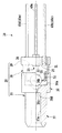
また、パッケージ28は、ステム29、キャップ部材30、および、スリーブ35から構成されている。上述のフォトダイオード22、前置増幅器24、コンデンサ25および26は、ステム29により支持されている。ステム29には、筒状のキャップ部材30が接合され、このキャップ部材30により、フォトダイオード22等が封止される。キャップ部材30は、集光用レンズ21をステム29上のフォトダイオード22と対向するように保持する。キャップ部材30には、集光用レンズ21と対向するように光コネクタのフェルール(光ファイバ)を保持し得るスリーブ35が接合される。
【0027】
受信用光モジュール20の構成および各構成部品について詳細に説明する。まず、ステム29は、半導体用パッケージの構成材料として一般的なFe(鉄)または表面にNiメッキを施したFeにより円盤状に形成されている。ステムの直径は、現状、最小値であると考えられる約3.8mmである。電子回路23の前置増幅器24やコンデンサ25および26をパッケージ28の外部に設けることにより、ステム29の更なる小径化も不可能ではないと考えられるが、本発明では、フォトダイオード22の出力信号に対する耐雑音特性を考慮し、電子回路23(フォトダイオード22、前置増幅器24、コンデンサ25および26)の全体が、パッケージ28の内部に収容される。ステム29の厚さは、およそ1mmであり、その部品搭載面は平坦に形成されている。
【0028】
また、ステム29には、図3および図4に示されるように、合計5本のリードピン40a〜40eが固定されている。受信用光モジュール20の5本のリードピン40a〜40eは、それぞれ、GND(接地)、VPD(受光素子電源)、VCC(増幅器電源)、Out(信号出力)、/Out(反転信号出力)に対応している。各リードピン40a〜40eは、Feまたは表面にNiメッキを施したFeまたはKoverにより形成されている。各リードピン40a〜40eの直径は、およそ0.3mmである。
【0029】
接地用のリードピン40aは、ステム29に溶接等により直接固定されている。一方、残り4本のリードピン40b〜40eは,ステム29に形成された直径およそ0.6〜0.75mmの孔に押通される。そして、各リードピン40b〜40eとステム29との隙間には、低融点ガラスが充填され、これにより、両者が互いに固定される。これらの4本のリードピン40b〜40eは、ステムの部品搭載面から、およそ0.35mm程度突出している。
【0030】
上述のように、接地用のリードピン40aは、ステム29に溶接等により直接固定されている。また、前置増幅器24、各コンデンサ25および26は、ステム29の部品搭載面に直接搭載(固定)されている。そして、これらの各部品24,25,26の離面(ステム29の部品搭載面と接する面)は、電極として機能するように構成されている。従って、ステム29の部品搭載面に固定された前置増幅器24、各コンデンサ25および26は、リードピン40aと接続され、これにより、前置増幅器24、コンデンサ25および26が接地されることになる。
【0031】
2体のコンデンサ25および26のうち、一方のコンデンサ25の上面には、フォトダイオード22がステム29の中央部に位置するように搭載(固定)される。すなわち、コンデンサ25の上面には、電極としての金属配線パターンが形成されており、フォトダイオード22のカソード電極Cは、この配線パターンに接続される。そして、コンデンサ25の上面の配線パターンは、受光素子電源用のリードピン40bにボンディングワイヤ(例えば、φ30〜50μmの金線)を介して接続されている。これにより、フォトダイオード22のカソード電極Cと受光素子電源用のリードピン40bとが、コンデンサ25を介して接続されることになる。フォトダイオード22には、コンデンサ25によって平滑化された電源信号が与えられる。
【0032】
一方、フォトダイオード22のアノード電極Aは、ボンディングワイヤを介して前置増幅器24の表面の配線パターンに接続されている。前置増幅器24の表面配線パターンに含まれる2つの出力端子は、ボンディングワイヤを介してリードピン40dおよび40eにそれぞれ接続されている。また、コンデンサ26の表面にも金属配線パターンが形成されている。コンデンサ26の配線パターンの一端は、ボンディングワイヤを介してリードピン40cに接続されており、コンデンサ26の配線パターンの他端は、ボンディングワイヤを介して前置増幅器24の表面の配線パターンに接続されている。これにより、前置増幅器24には、コンデンサ26によって平滑化された電源信号が与えられる。
【0033】
このような構成のもとでは、光コネクタ(光ファイバ)からの光信号は、フォトダイオード22によって光−電気変換され、電流信号として前置増幅器24に送出される。図5からわかるように、前置増幅器24は、いわゆるトランスインピーダンスアンプTIAおよびトランスインピーダンスTIを含むようにモノリシックに構成されている。また、トランスインピーダンスTIの抵抗値は、数kΩ〜50kΩ程度である。従って、フォトダイオード22が発生する電流信号の大部分は、前置増幅器24の入力インピーダンスが非常に高いことに起因して、トランスインピーダンスTIに流入する。そして、トランスインピーダンスTIに電流が流れ込むと、トランスインピーダンスTIの両端に電圧が発生する。これにより、フォトダイオード22からの電流信号は、電圧信号に変換される。これと同時に、前置増幅器24は、入力電流信号と位相が180°異なるように相補信号を生成する。この結果、リードピン40dからOut信号が、リードピン40eから/Out信号が送出されることになる。
【0034】
なお、本実施形態では、前置増幅器24は、一辺の長さが0.3〜0.5mm程度の長方形状の平面形状を有し、その厚さは、0.3〜0.4mm程度とされている。前置増幅器24としては、光信号周波数が数百MHz程度である場合、SiバイポーラICが用いられてもよく、光信号周波数が1GHzを越える場合には、GaAsデバイスが、10GHzを越える場合には、SiGeInPを素材とするICが用いられる。
【0035】
また、本実施形態では、コンデンサ25および26として、容量が100〜2200pF程度の平行平板型コンデンサが採用されている。受光素子電源用のリードピン40bと接地用のリードピン40aとの間に配置されるコンデンサ25は、長方形状の平面形状を有する一方、増幅器電源用のリードピン40cと接地用のリードピン40aとの間に配置されるコンデンサ26は、一辺の長さが0.5mm程度の正方形状の平面形状を有する。各コンデンサ25および26の厚さは、0.2〜0.4mm程度である。
【0036】
更に、本実施形態では、フォトダイオード22として、InPを基板材料とするInGaAs系の面受光PIN−フォトダイオードが採用されている。InGaAs系材料は、InおよびGaの構成比率を変化させることにより、光通信の主要な波長帯である1.3μmおよび1.55μmの双方に対応可能なものである。フォトダイオード22は、一辺の長さが0.3〜0.5mmの正方形状の平面形状を有し、その厚さは、0.1〜0.3mm程度である。光に感度を有する受光面は、直径30〜50μmの円形とされている。
【0037】
さて、ステム29上のフォトダイオード22や電子回路23を覆うキャップ部材30は、厚さ0.15mm程度のFe(鉄)または表面にNiメッキを施したFeにより筒状に形成されている。本実施形態では、キャップ部材30の全高Hは、およそ2.7mmである。また、キャップ部材30は、図6に示されるように、その頂部に、集光用レンズ21を保持するための開口30aを有する。本実施形態では、集光用レンズ21は、直径およそ1.5mmの球形に形成されていることから、開口30aの内径もそれに適合させるべく、およそ1.5mm+αに設定されている。集光用レンズ21が固定されたキャップ部材30は、集光用レンズ21によって、光コネクタ(光ファイバ)からの光信号がステム29上のフォトダイオード22の受光面に精度よく集光されるように、ステム29に接合される。
【0038】
ここで、本発明の光モジュール20においては、このキャップ部材30の形状に改良が施されている。すなわち、図3および図6に示されるように、キャップ部材30は、ステム29側に位置する直径φ1の円筒状の大径部31と、集光用レンズ21側に位置する直径φ2の円筒状の小径部32とを含む。本実施形態では、大径部31の直径φ1が、ステム29の直径に適合するように、およそ3.5mmとされている。また、大径部31の内部の高さH1は、フォトダイオード22を含む電子回路23を収容するのに必要十分となるように、およそ0.7mmとされている。これに対して、小径部32の直径φ2は、大径部31の直径φ1よりも小さく定められている。本実施形態では、小径部32の直径φ2は、直径およそ1.5mmの球形レンズ21を開口30a内に固定することを考慮して、およそ2.6mmまで小径化されている。なお、集光用レンズ21の直径を更に小径化すれば、小径部32の更なる小径化を図ることも可能ではある。
【0039】
そして、本発明による光モジュール20では、図3に示されるように、キャップ部材30の小径部32とスリーブ35とが紫外線硬化樹脂等により互いに接合される。スリーブ35は、樹脂または金属により概ね円筒状に形成され、円筒状の接続部36と、接続部36よりも小径の円筒状のフェルール保持部37とを有する。接続部36は、内部に空洞部36aを有し、この空洞部36a内に、上述のキャップ部材30の小径部32が挿入・固定される。本実施形態では、空洞部36aの内径は、光コネクタの光ファイバとフォトダイオード22とをX−Y平面(光軸に垂直な平面)において調芯する際の調整代が確保されるように、およそ3.1mmとされ、その深さは、およそ1.5mmとされている。
【0040】
このように、キャップ部材30の小径部32とスリーブ35の接続部36とを接合させる構成を採用することにより、ステム29の最大外径を定める接続部36の外径をステム29の外径(3.8mm)よりも多少大きい程度のおよそ4.0mmとすることが可能となる。もちろん、接続部36aの側壁を更に薄肉化することにより、接続部36の更なる小径化(4.0mm以下)も可能である。
【0041】
スリーブ35のフェルール保持部37は、接続部36から延出されている。フェルール保持部37は、接続部36の空洞部36aとは反対側に開放されたフェルール挿入孔37aを有する。フェルール保持部37(フェルール挿入孔37a)の寸法は、接続対象となる光コネクタの規格に基づいて定められる。すなわち、本実施形態では、外径1.25mmのフェルールを備えたLC型光コネクタに適合するように、フェルール保持部37の外径は、およそ2.8mmとされ、その全長は、およそ4.5mmとされる。また、フェルール挿入孔37aの内径は、1.25mm+2μmとされている。これにより、フェルール挿入孔37aに光コネクタのフェルールを挿入するだけで、光軸の調心が可能となる。
【0042】
図3に示されるように、スリーブ35の接続部36の内部には、集光用レンズ21を収納するために、円錐面状を呈する凹部36bが形成されている。そして、この凹部36bは、接続部36に形成された連通孔36cを介してフェルール挿入孔37aと連通している。連通孔36cの内径は、およそ0.4mm、その長さは、およそ1.0mmである。光コネクタのフェルールがフェルール挿入孔37aに挿入されると、フェルールの先端面は、接続部36の端面36dに突き当たる。
【0043】
次に、上述された光モジュール20の製造方法について簡単に説明する。まず、ステム29には、リードピン40a〜40eが上述の手法により、所定位置に固定される。また、ステム29の部品搭載面には、フォトダイオード22等を含む電子回路23が搭載される。この場合、前置増幅器24、コンデンサ25および26の裏面(接地面)に導電性接着剤を塗布し、ステム29上の所定位置に載置する。更に、フォトダイオード22の裏面にも導電性接着剤を塗布し、コンデンサ25の表面の所定位置に載置する。そして、導電性接着剤の溶剤を揮発させるべく、各部品に熱処理を施す。電子回路23の構成部品がステム29上に接着されたならば、フォトダイオード22、前置増幅器24、各コンデンサ25および26を対応するリードピン40b〜40eにボンディングワイヤにより結線する。
【0044】
次に、ステム29に、キャップ部材30が抵抗溶接により接合される。すなわち、キャップ部材30のステム29側の端部には、図6に示されるように、断面三角形状の突起31aが全周にわたって形成されている。キャップ部材30をステム29に接合するに際しては、この突起31aをステム29に突き当てた状態で、両者の接触部に大電流を供給する。これにより、突起31aの頂部における電流密度が高まり、突起31aが局所的に溶融し、キャップ部材30がステム29に溶着する。この溶接作業は、不活性ガス(窒素)雰囲気中で行われる。なお、ここまでの作業においては、個別の調芯作業は行われず、調心は、各部品の寸法精度のみに依存する。また、ステム29への接合前に、キャップ部材30の開口30aには、集光用レンズ21が低融点ガラス等からなるペレット等を用いて予め固定されている。
【0045】
ステム29にキャップ部材30が固定されたならば、キャップ部材30の小径部32にスリーブ35を接合する。この場合、まず、キャップ部材30の小径部32の外周面と、接続部36内の空洞部36aとに遅効性接着剤を塗布した上で、小径部32を空洞部36aに挿入する。次に、実際に光ファイバ中に光信号を通過させた状態で、光コネクタのフェルールをスリーブ35のフェルール挿入孔37aに挿入する。更に、光信号を光ファイバから出射させ、集光用レンズ21を介してフォトダイオード22に受光させる。そして、フォトダイオード22における受光状態をモニタリングしながら、キャップ部材30とスリーブ35との係合状態を調節する。この調節作業により最適位置が決定されたならば、そのまま状態で各部品を固定し、接着剤を硬化させる。これにより、光モジュール20が完成する。
【0046】
上述されたように、本発明による光モジュール20では、キャップ部材30が、ステム29側に、外径φ1を有する大径部31を含む一方、集光用レンズ21側に、大径部31の外径φよりも小さい外径φ2を有する小径部32を含んでいる。そして、キャップ部材30の小径部32とスリーブ35とが互いに接合される。これにより、キャップ部材30の大径部31の外径φ1を、ステム29の外径に適合させると共にフォトダイオード22を含む電子回路23の収容容積が必要十分に確保されるように設定することができる。そして、キャップ部材30の小径部32の外径φ2を、集光用レンズ21の固定に支障のない範囲でできるだけ小さく定めることができる。
【0047】
このように、キャップ部材30の集光用レンズ21側(光ファイバ側)の径を小径化することにより、スリーブ35自体の強度およびキャップ部材30とスリーブ35との接着強度を確保するために、スリーブの肉厚(接続部36の側壁の厚さ)をある程度確保したとしても、スリーブ35の最大外径(接続部36の外径)をステム29の外径とほぼ同程度、あるいは、それ以下にまで小さくすることが可能となる。すなわち、本発明の構成を採用することにより、スリーブ35の最大外径を、4mm以下にすることが可能となる。この結果、本発明によれば、回路基板上における光モジュール20の実装密度をより一層高めることが可能となるとと共に、このような光モジュール20を備えた光送受信器1全体のコンパクト化、すなわち、光送受信器1の実装密度の向上を容易に実現することができる。
【0048】
なお、詳細な説明は省略するが、本実施形態における光送受信器1では、電子回路に入力する電気信号を光信号に変換する発光素子を備える送信用光モジュール20Aも、受信用光モジュール20と同様に、大径部と小径部とを含むキャップ部材を有している。これにより、送信用光モジュール20Aもコンパクト化されることから、本発明による光送受信器1では、全体のパッケージを容易にコンパクト化することができる。
【0049】
図7は、本発明による他の実施形態を示す部分断面図である。なお、上述の実施形態に関連して説明された要素と同一の要素については、同一の符号を付し、重複する説明は省略する。
【0050】
図7に示される受信用光モジュール20Bでは、キャップ部材30の小径部32に加えて、キャップ部材30の大径部31も、スリーブ35と互いに接合されている。すなわち、本実施形態では、スリーブ35の接続部36のステム29側に位置する端部には、薄肉の延出部36eが形成されている。そして、この延出部36eとキャップ部材30の大径部31とが互いに接合されている。本実施形態では、延出部36eの内径は、およそ3.8mmとされ、その深さは、およそ1.3mmとされている。また、延出部36eの外径は、およそ4.0mmとされる。すなわち、延出部36eは、接続部36から面一に延出されている。このような構成を採用することにより、スリーブ35の最大外径の増加を抑制しつつ、キャップ部材30とスリーブ35との接合強度をより一層高めることが可能となる。
【0051】
【発明の効果】
以上説明されたように、本発明によれば、コンパクトなパッケージを有し、回路基板上における実装密度を高めることができる光モジュールの実現が可能となる。
【図面の簡単な説明】
【図1】 本発明が適用される光送受信器を示す斜視図である。
【図2】図1に示される光送受信器の分解斜視図である。
【図3】図1の光送受信器に含まれる本発明の光モジュールを示す部分断面図である。
【図4】図4の光モジュールに含まれるステム周辺の構成を示す斜視図である。
【図5】図4の光モジュールの回路構成を示す回路図である。
【図6】図4の光モジュールを構成するキャップ部材を示す断面図である。
【図7】本発明による光モジュールの他の実施形態を示す部分断面図である。
【符号の説明】
1 光送受信器
2 レセプタクル
3 ハウジング
4 ハウジング本体
5 カバー部材
20,20B 受信用光モジュール
20A 送信用光モジュール
21 集光用レンズ
22 フォトダイオード
23 電子回路
24 前置増幅器
25,26 コンデンサ
28 パッケージ
29 ステム
30 キャップ部材
31 大径部
32 小径部
35 スリーブ
36 接続部
36a 空洞部
36e 延出部
37 フェルール保持部
37a フェルール挿入孔
40a,40b,40c,40d,40e リードピン[0001]
BACKGROUND OF THE INVENTION
The present invention relates to an optical module. Le In particular, an optical module capable of receiving or transmitting optical signals. Le Related.
[0002]
[Prior art]
Conventionally, what was disclosed by Unexamined-Japanese-Patent No. 7-31430 is known as a technique of this kind of field. This publication discloses a light receiving module capable of converting an optical signal input via an optical fiber into an electric signal. The light receiving module described in the publication has a condensing lens, a light receiving element such as a photodiode, a preamplifier, and an electronic circuit including a capacitor. These components are included in a cylindrical package (PKG). Is housed in. In this case, a ferrule attached to the optical fiber is connected (inserted) to one end of the package. In addition, lead pins for transmitting and receiving electric signals are extended from the other end of the package. That is, in this optical module, the extending direction of the optical fiber and the extending direction of the lead pin are substantially parallel. For this reason, such an optical module is generally called a coaxial optical module.
[0003]
In the coaxial optical module as described above, a discrete semiconductor package (so-called TO type PKG) including a transistor is used as a package. Such a package includes a stem (substrate), a cap member, and a sleeve. The electronic circuit described above is mounted on the stem and is electrically connected to a plurality of lead pins. These lead pins extend outward from the stem. The electronic circuit including the photoelectric conversion element on the stem is sealed with a cap member joined to the stem. The cap member holds the lens so as to face the photoelectric conversion element. A sleeve formed of resin or the like is joined to the cap member. The sleeve has a hole for inserting the ferrule described above. When the ferrule is inserted into the hole of the sleeve, the optical fiber on the ferrule side and the photoelectric conversion element in the cap member can be optically coupled via the lens.
[0004]
[Problems to be solved by the invention]
By the way, in recent years, optical communication using the above-described optical module has rapidly spread. With the spread of optical communication, the application range of optical modules has been extended to, for example, communication between back panels of computers that have been used for telecommunications, communication between telephone exchanges, and the like. In such an application, it is necessary to arrange a large number of optical modules and an optical transceiver having the optical modules on an integrated circuit board. In this case, as the number of optical modules and optical transceivers increases, how to improve the mounting density of the optical modules or how to make the optical transceiver equipped with the optical modules compact. It becomes.
[0005]
The present invention has been made in view of such circumstances, and has an optical module that has a compact package and can increase the mounting density on a circuit board. Le For the purpose of provision.
[0006]
[Means for Solving the Problems]
One embodiment of the present invention relates to an optical module including a lens and an electronic circuit including a photoelectric conversion element. The optical module is capable of performing conversion from one of an optical signal and an electric signal to the other by a photoelectric conversion element, and includes a package including a stem, a cap member, and a sleeve. That is, the electronic circuit including the photoelectric conversion element is supported by the stem. A cylindrical cap member is joined to the stem, and the cap member holds the lens so as to face the photoelectric conversion element on the stem. A sleeve capable of holding an optical fiber (ferrule) is joined to the cap member so as to face the lens.
[0007]
Here, for this type of optical module, it is required to increase the mounting density on the circuit board. The mounting density of this type of optical module mainly depends on the outer diameter of the ferrule. At present, the outer diameter of the ferrule is reduced to about 1.25 mm, and the stem constituting the package is also reduced in diameter in accordance with the outer diameter of the ferrule. For example, in accordance with such a small-diameter ferrule, for example, a stem having an outer diameter of 3.8 mm is also used.
[0008]
However, while keeping the outer diameter of the cap appropriately with respect to the stem diameter, and maintaining the strength of the sleeve itself and the bonding portion between the sleeve and the cap, the package can be made even if the thickness of the sleeve is made as thin as possible. It is not easy to reduce the outer diameter of the sleeve that determines the maximum outer diameter. For example, even if the outer diameter of the stem is reduced to about 3.8 mm, it has been difficult to reduce the outer diameter of the sleeve to 4.5 mm or less. Thus, conventionally, the difficulty in reducing the diameter of the sleeve has prevented the optical modules from being arranged on the circuit board at a higher density.
[0009]
In this case, it is substantially difficult to further reduce the outer diameter of the stem. That is, an electronic circuit including a photoelectric conversion element or the like must be mounted on the stem. In addition to this, the stem needs to be provided with a plurality of lead pins in order to exchange electrical signals with the electronic circuit. For example, three lead pins are required for the transmission optical module and five for the reception optical module (GND, VPD, VCC, OVT, / OUT). On the other hand, in order to reduce the diameter of the stem, it may be possible to arrange a preamplifier, a capacitor, and the like constituting the electronic circuit outside the package. However, this is not practical because the signal from the photoelectric conversion element becomes weak or it is difficult to ensure noise resistance. Therefore, in order to satisfy these conditions, it is necessary to further downsize the package while maintaining at least the outer diameter of the stem at the current minimum value of about 3.8 mm.
[0010]
Based on such a background, the present inventors have intensively studied to increase the mounting density of the optical module, and as a result, have come to focus on the cap member disposed between the stem and the sleeve. In the optical module, the shape of the cap member was improved. That is, the cap member of the optical module according to the present invention has a large-diameter portion having a first outer diameter that is joined to the stem at one end side to accommodate the electronic circuit, and smaller than the first outer diameter of the large-diameter portion. And a small diameter portion having a second outer diameter. That is, the cross-sectional area of the small diameter part is smaller than the cross-sectional area of the large diameter part. The sleeve includes a cylindrical connection portion having an inner diameter larger than the small diameter portion of the cap member and into which the small diameter portion is inserted, and a ferrule holding portion capable of holding the optical fiber. Then, the small diameter portion of the cap member and the connecting portion of the sleeve are joined to each other via an adhesive. The outer diameter of the large diameter part of the cap member and the connecting part of the sleeve is less than the outer diameter of the stem. The
[0011]
The outer diameter (first outer diameter) of the large-diameter portion of the cap member is set so as to match the outer diameter of the stem, and to ensure a necessary and sufficient storage capacity of the electronic circuit including the photoelectric conversion element. On the other hand, the outer diameter (second outer diameter) of the small-diameter portion of the cap member is determined as small as possible within a range that does not hinder the fixing of the lens. In this way, by reducing the diameter of the cap member on the lens side (optical fiber side), in order to ensure the strength of the sleeve itself and the adhesive strength between the cap member and the sleeve, the thickness of the sleeve at the bonding location is reduced. Even if it is secured to some extent, the maximum outer diameter of the sleeve can be reduced to approximately the same as or less than the outer diameter of the stem. As a result, according to the present invention, the optical module package can be made compact, and the mounting density of the optical modules on the circuit board can be easily increased.
[0012]
Further, the large diameter portion of the cap member and the sleeve may be joined to each other. This place If Sleeve The connecting portion has a larger inner diameter than the large-diameter portion of the cap member and the large-diameter portion is inserted. Extension On its tip Formed, this Extension And large The diameter is Through the adhesive Joined together This When But preferable. Accordingly, it is possible to increase the bonding strength between the cap member and the sleeve while suppressing an increase in the maximum outer diameter of the sleeve.
[0013]
By adopting these configurations , Yo More specifically, the maximum outer diameter of the sleeve can be 4 mm or less. As a result, according to the present invention, the mounting density of the optical module on the circuit board can be further increased.
[0014]
Furthermore, the photoelectric conversion element is preferably a light receiving element that converts an optical signal input via an optical fiber into an electric signal. In this case, it is preferable that the electronic circuit further includes a preamplifier that amplifies the electric signal from the light receiving element and a capacitor that smoothes the power signal to the light receiving element and the preamplifier.
[0015]
In addition, the photoelectric conversion element may be a light emitting element that converts an electrical signal input to an electronic circuit into an optical signal.
[0017]
Also By applying the optical module of the present invention as a receiving optical module of an optical transceiver, it becomes possible to easily realize a compact optical transceiver. Of course, in such an optical transceiver, it goes without saying that the optical module of the present invention can be applied as a transmission optical module.
[0018]
DETAILED DESCRIPTION OF THE INVENTION
Hereinafter, an optical module according to the present invention will be described with reference to the drawings. Le Preferred embodiments will be described in detail.
[0019]
FIG. 1 shows the present invention. Subject to FIG. 2 is an exploded perspective view of the optical transceiver shown in FIG. 1. The
[0020]
As shown in FIGS. 1 and 2, the
[0021]
The wall surface of the
[0022]
The reception
[0023]
A terminal pin group 9 is arranged on the housing body 4. The reception circuit board 7 and the transmission circuit board 8 are electrically connected to the circuit board on which the
[0024]
3 to 6 show an optical module provided in the
[0025]
As shown in FIG. 3, the receiving
[0026]
The
[0027]
The configuration of the receiving
[0028]
In addition, as shown in FIGS. 3 and 4, a total of five
[0029]
The
[0030]
As described above, the
[0031]
Of the two
[0032]
On the other hand, the anode electrode A of the
[0033]
Under such a configuration, an optical signal from the optical connector (optical fiber) is photoelectrically converted by the
[0034]
In the present embodiment, the
[0035]
In the present embodiment, parallel plate capacitors having a capacitance of about 100 to 2200 pF are employed as the
[0036]
Furthermore, in this embodiment, an InGaAs-based surface light-receiving PIN-photodiode using InP as a substrate material is employed as the
[0037]
Now, the
[0038]
Here, in the
[0039]
And in the
[0040]
In this way, by adopting a configuration in which the
[0041]
The
[0042]
As shown in FIG. 3, a
[0043]
Next, a method for manufacturing the above-described
[0044]
Next, the
[0045]
When the
[0046]
As described above, in the
[0047]
Thus, in order to ensure the strength of the
[0048]
Although detailed explanation is omitted, this book Embodiment In Oke In the
[0049]
FIG. 7 is a partial cross-sectional view showing another embodiment according to the present invention. In addition, the same code | symbol is attached | subjected about the element same as the element demonstrated in relation to the above-mentioned embodiment, and the overlapping description is abbreviate | omitted.
[0050]
In the receiving
[0051]
【The invention's effect】
As described above, according to the present invention, an optical module having a compact package and capable of increasing the mounting density on a circuit board. Le Realization is possible.
[Brief description of the drawings]
FIG. 1 shows the present invention. Is applied 1 is a perspective view showing an optical transceiver.
FIG. 2 is an exploded perspective view of the optical transceiver shown in FIG.
3 is a partial cross-sectional view showing an optical module of the present invention included in the optical transceiver of FIG. 1. FIG.
4 is a perspective view showing a configuration around a stem included in the optical module of FIG. 4; FIG.
5 is a circuit diagram showing a circuit configuration of the optical module of FIG. 4;
6 is a cross-sectional view showing a cap member constituting the optical module of FIG. 4;
FIG. 7 is a partial cross-sectional view showing another embodiment of the optical module according to the present invention.
[Explanation of symbols]
1 Optical transceiver
2 Receptacle
3 Housing
4 Housing body
5 Cover members
20, 20B Receiving optical module
20A optical module for transmission
21 Condensing lens
22 Photodiode
23 Electronic circuit
24 Preamplifier
25, 26 capacitors
28 packages
29 stem
30 Cap member
31 Large diameter part
32 Small diameter part
35 sleeve
36 connections
36a Cavity
36e extension part
37 Ferrule holder
37a Ferrule insertion hole
40a, 40b, 40c, 40d, 40e Lead pin
Claims (2)
前記光電変換素子を含む前記電子回路を支持するステムと、
前記レンズを前記光電変換素子と対向するように保持する筒状のキャップ部材と、
前記レンズと対向するように光ファイバを保持し得るスリーブとを備え、
前記キャップ部材は、その一端側が前記ステムに接合されて前記電子回路を収容する第1の外径を有する大径部と、この大径部の第1の外径よりも小さな第2の外径を有する小径部とを含み、
前記スリーブは、前記キャップ部材の小径部よりも大きな内径を有すると共にこの小径部が挿入される円筒状の接続部と、前記光ファイバを保持し得るフェルール保持部とを含み、
前記キャップ部材の小径部と前記スリーブの接続部とが接着剤を介して互いに接合され、
前記キャップ部材の大径部および前記スリーブの接続部の外径は、前記ステムの外径以下であることを特徴とする光モジュール。In an optical module having a lens and an electronic circuit including a photoelectric conversion element, and performing conversion from one of an optical signal and an electrical signal to the other by the photoelectric conversion element,
A stem that supports the electronic circuit including the photoelectric conversion element;
A cylindrical cap member for holding the lens so as to face the photoelectric conversion element;
A sleeve capable of holding an optical fiber so as to face the lens,
The cap member has a large-diameter portion having a first outer diameter in which one end side is joined to the stem and accommodates the electronic circuit, and a second outer diameter smaller than the first outer diameter of the large-diameter portion. A small-diameter portion having
The sleeve includes a cylindrical connecting portion having an inner diameter larger than a small diameter portion of the cap member and into which the small diameter portion is inserted, and a ferrule holding portion capable of holding the optical fiber,
The small diameter portion of the cap member and the connecting portion of the sleeve are joined together via an adhesive ,
The outer diameter of the connecting portion of the large diameter portion and the sleeve of the cap member, the light module, wherein the outer diameter or under der Rukoto of the stem.
Priority Applications (1)
| Application Number | Priority Date | Filing Date | Title |
|---|---|---|---|
| JP2002039166A JP3972677B2 (en) | 2002-02-15 | 2002-02-15 | Optical module |
Applications Claiming Priority (1)
| Application Number | Priority Date | Filing Date | Title |
|---|---|---|---|
| JP2002039166A JP3972677B2 (en) | 2002-02-15 | 2002-02-15 | Optical module |
Publications (2)
| Publication Number | Publication Date |
|---|---|
| JP2003241031A JP2003241031A (en) | 2003-08-27 |
| JP3972677B2 true JP3972677B2 (en) | 2007-09-05 |
Family
ID=27780277
Family Applications (1)
| Application Number | Title | Priority Date | Filing Date |
|---|---|---|---|
| JP2002039166A Expired - Fee Related JP3972677B2 (en) | 2002-02-15 | 2002-02-15 | Optical module |
Country Status (1)
| Country | Link |
|---|---|
| JP (1) | JP3972677B2 (en) |
Families Citing this family (7)
| Publication number | Priority date | Publication date | Assignee | Title |
|---|---|---|---|---|
| JP2006106504A (en) * | 2004-10-07 | 2006-04-20 | Nippon Electric Glass Co Ltd | Optical cap component |
| JP2007121920A (en) * | 2005-10-31 | 2007-05-17 | Sony Corp | Optical module, optical communication module, and optical communication device |
| JP4765563B2 (en) * | 2005-11-07 | 2011-09-07 | セイコーエプソン株式会社 | Optical module |
| JP4583438B2 (en) * | 2007-12-28 | 2010-11-17 | 日本オプネクスト株式会社 | Optical receptacle, optical module, and optical module manufacturing method |
| JP2009192566A (en) * | 2008-02-12 | 2009-08-27 | Sumitomo Electric Ind Ltd | Optical sub-assembly |
| JP5060419B2 (en) * | 2008-07-30 | 2012-10-31 | 株式会社エンプラス | Manufacturing method of optical receptacle |
| JP2012194583A (en) * | 2012-07-09 | 2012-10-11 | Enplas Corp | Optical receptacle kit |
-
2002
- 2002-02-15 JP JP2002039166A patent/JP3972677B2/en not_active Expired - Fee Related
Also Published As
| Publication number | Publication date |
|---|---|
| JP2003241031A (en) | 2003-08-27 |
Similar Documents
| Publication | Publication Date | Title |
|---|---|---|
| US5814871A (en) | Optical semiconductor assembly having a conductive float pad | |
| JP3047735B2 (en) | Optical receiving module and method of manufacturing the same | |
| US6795461B1 (en) | Optoelectric module | |
| US6074102A (en) | Optical device capable of operating at high speeds | |
| US20120057879A1 (en) | Discrete bootstrapping in an optical receiver to prevent signal feedback | |
| US20030147601A1 (en) | Hybrid optical module employing integration of electronic circuitry with active optical devices | |
| US20030102157A1 (en) | Circuit interconnect for optoelectronic device for controlled impedance at high frequencies | |
| JP2006253676A (en) | Optical assembly | |
| CN110380787A (en) | Receiver assembly | |
| US20060133739A1 (en) | Silicon optical bench-based optical sub-assembly and optical transceiver using the same | |
| JP5125235B2 (en) | Optical transceiver and optical transceiver module | |
| JP3972677B2 (en) | Optical module | |
| US11482559B2 (en) | Optical semiconductor device and method of assembling optical semiconductor device | |
| JP4828103B2 (en) | Optical transceiver module | |
| JP2007242708A (en) | Light receiving subassembly | |
| US6948863B2 (en) | Optical module and optical transceiver module | |
| US7226219B2 (en) | High-frequency signal transmitting optical module and method of fabricating the same | |
| JP2003241029A (en) | Optical module and optical transmitter receiver | |
| CN108574018B (en) | Optical receiving module and optical module | |
| JP2004071890A (en) | Optical module | |
| JP2941303B2 (en) | Optical front-end device | |
| JP2004363360A (en) | Optical transmitting and receiving module | |
| JP2004095869A (en) | Light receiving element and light receiving device | |
| JP2004254125A (en) | Light receiving module | |
| JP2715672B2 (en) | Optical semiconductor photodetector with built-in preamplifier |
Legal Events
| Date | Code | Title | Description |
|---|---|---|---|
| A621 | Written request for application examination |
Free format text: JAPANESE INTERMEDIATE CODE: A621 Effective date: 20050214 |
|
| A977 | Report on retrieval |
Free format text: JAPANESE INTERMEDIATE CODE: A971007 Effective date: 20061115 |
|
| A131 | Notification of reasons for refusal |
Free format text: JAPANESE INTERMEDIATE CODE: A131 Effective date: 20061124 |
|
| A521 | Request for written amendment filed |
Free format text: JAPANESE INTERMEDIATE CODE: A523 Effective date: 20070118 |
|
| RD04 | Notification of resignation of power of attorney |
Free format text: JAPANESE INTERMEDIATE CODE: A7424 Effective date: 20070118 |
|
| A131 | Notification of reasons for refusal |
Free format text: JAPANESE INTERMEDIATE CODE: A131 Effective date: 20070209 |
|
| A521 | Request for written amendment filed |
Free format text: JAPANESE INTERMEDIATE CODE: A523 Effective date: 20070410 |
|
| TRDD | Decision of grant or rejection written | ||
| A01 | Written decision to grant a patent or to grant a registration (utility model) |
Free format text: JAPANESE INTERMEDIATE CODE: A01 Effective date: 20070522 |
|
| A61 | First payment of annual fees (during grant procedure) |
Free format text: JAPANESE INTERMEDIATE CODE: A61 Effective date: 20070604 |
|
| R150 | Certificate of patent or registration of utility model |
Free format text: JAPANESE INTERMEDIATE CODE: R150 |
|
| FPAY | Renewal fee payment (event date is renewal date of database) |
Free format text: PAYMENT UNTIL: 20100622 Year of fee payment: 3 |
|
| FPAY | Renewal fee payment (event date is renewal date of database) |
Free format text: PAYMENT UNTIL: 20110622 Year of fee payment: 4 |
|
| FPAY | Renewal fee payment (event date is renewal date of database) |
Free format text: PAYMENT UNTIL: 20110622 Year of fee payment: 4 |
|
| FPAY | Renewal fee payment (event date is renewal date of database) |
Free format text: PAYMENT UNTIL: 20120622 Year of fee payment: 5 |
|
| FPAY | Renewal fee payment (event date is renewal date of database) |
Free format text: PAYMENT UNTIL: 20130622 Year of fee payment: 6 |
|
| R250 | Receipt of annual fees |
Free format text: JAPANESE INTERMEDIATE CODE: R250 |
|
| R250 | Receipt of annual fees |
Free format text: JAPANESE INTERMEDIATE CODE: R250 |
|
| LAPS | Cancellation because of no payment of annual fees |