EP0681368B1 - Amplificateur opérationnel à taux élevé de rejection de mode commun - Google Patents
Amplificateur opérationnel à taux élevé de rejection de mode commun Download PDFInfo
- Publication number
- EP0681368B1 EP0681368B1 EP95106851A EP95106851A EP0681368B1 EP 0681368 B1 EP0681368 B1 EP 0681368B1 EP 95106851 A EP95106851 A EP 95106851A EP 95106851 A EP95106851 A EP 95106851A EP 0681368 B1 EP0681368 B1 EP 0681368B1
- Authority
- EP
- European Patent Office
- Prior art keywords
- output
- operational amplifier
- stage
- balanced
- input
- Prior art date
- Legal status (The legal status is an assumption and is not a legal conclusion. Google has not performed a legal analysis and makes no representation as to the accuracy of the status listed.)
- Expired - Lifetime
Links
Images
Classifications
-
- H—ELECTRICITY
- H03—ELECTRONIC CIRCUITRY
- H03F—AMPLIFIERS
- H03F3/00—Amplifiers with only discharge tubes or only semiconductor devices as amplifying elements
- H03F3/45—Differential amplifiers
- H03F3/45071—Differential amplifiers with semiconductor devices only
- H03F3/45479—Differential amplifiers with semiconductor devices only characterised by the way of common mode signal rejection
Definitions
- the invention relates to an operational amplifier with symmetrical Inputs and balanced outputs.
- Such an operational amplifier is from the German Utility model G 92 07 812.5 known.
- the one described therein Circuit arrangement is for a supply voltage of designed for a minimum of 4.5 volts. More modern circuit arrangements however, require one especially in mobile applications minimum supply voltage of 2.7 volts.
- the well-known Amplifier circuit is designed for 4.5 volts, it contains Cascode levels for high no-load gain and low-resistance "Pushpull" output buffer amplifier. These circuit parts stand in the way of operation at 2.7 volts because of the arrangement up to 4 diode threshold voltages added up.
- a differential amplifier is known from the prior art US Pat. No. 5,298,809 known with two differential outputs. This is but also not for operation with low supply voltages, d. H. suitable at 2.7 volts.
- the object of the present invention is therefore an operational amplifier specify the at a high common mode rejection has a lower supply voltage.
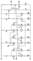
- the operational amplifier shown as an exemplary embodiment are two emitter followers 3, 4 as a symmetrical output stage provided, whose emitters each have output connections 39, 40 are connected to the outputs of the operational amplifier form.
- These emitter followers replace the known ones "Pushpull" - output buffer amplifier.
- Between the output ports of the two emitter followers 3, 4 is one of two in Series of switched resistors 1, 2 existing voltage dividers switched.
- the resistors 1, 2 have identical ones Resistance values so that the division factor of the voltage divider is equal to 0.5.
- Voltage division can also be used for certain Applications, especially for frequency compensation also voltage dividers provided with inductive or capacitive components become.
- the emitter followers are each over on the emitter side one current source 37, 38 each with a first supply voltage terminal 41 connected.
- the collectors of the emitter followers 3, 4 are each with a further supply voltage terminal 42 interconnected.
- the base connections of the two emitter followers 3, 4 are each connected via a current source 31, 32 coupled to the positive supply potential 42 and another connected to the collector of an npn transistor 33, 34.
- the emitters of the two transistors 33, 34 are over each have a resistor 35, 36 to the negative supply potential 41 out.
- the bases of the two transistors 33, 34 are each with the base and collector of an NPN transistor 13, 14 connected, the emitters of which in turn each have a resistor 11, 12 with the negative supply potential 41 are connected.
- the interconnected bases and collectors of the NPN transistors 13, 14 are also included the collector of a pnp transistor 5, 6 connected.
- the emitters of the two pnp transistors 5, 6 are together and via a current source 7 to the positive supply potential 42 connected.
- the collector of the pnp transistor 5 with the Collectors of a pnp transistor 15 and an npn transistor 19 connected.
- a pnp transistor is in parallel with transistor 15 16 provided the collector with an npn transistor 20 is connected.
- the emitters of the transistors 19 and 20 are each connected via a resistor 21, 22 to the negative supply potential 41 connected.
- the basic connections the npn transistors 19, 20 are with each other and with connected to the collector of transistor 20.
- the emitter of the PNP transistors 15, 16 are with each other and via a current source 17 coupled to the positive supply potential 42.
- At the base of the pnp transistor 15 is a Reference potential 19 on.
- the base of the pnp transistor 15 is connected to the Base of another pnp transistor 23 connected.
- the The base of transistor 16 is also at the base of another pnp transistor 24 coupled.
- the two emitters of the Transistors 23 and 24 are with each other and through a current source 25 coupled to the positive supply potential 42.
- the collector of transistor 23 is on the one hand with the collector of the transistor 14 and the other with the collector of another npn transistor 27 connected.
- the collector the pnp transistor 24 is connected to the collector of another npn transistor 28 coupled.
- the base connections of the NPN transistors 27 and 28 are with each other and with the collector of transistor 28 connected.
- the two emitter connections of transistors 27 and 28 are each through a resistor 29 and 30 coupled to the negative supply potential 41.
- the base of the pnp transistor 16 is connected to the Tap of the voltage divider forming the node between the resistors 1 and 2 connected.
- a second differential amplifier stage consisting of two in parallel switched differential amplifiers 15 to 22 and 23 to 30 with a reference value at the input terminal 19 is compared.
- This differential amplifier stage exists in the present exemplary embodiment essentially from the two pnp transistors 15, 16, and the associated power sources 17.
- the second amplifier stage connected in parallel consists of the two pnp transistors 23, 24 and the associated current source 25.
- a first differential amplifier stage for example corresponds to the aforementioned, which is essentially by the pnp transistors 5, 6 and the current source 7 is formed, is a symmetrical via the inputs 9, 10 Input signal supplied.
- This differential amplifier stage is completed by a load.
- the load is in the present Case formed by two current mirrors, each with one Output terminal of the first differential amplifier stage coupled are.
- the two current mirrors each form one Load that terminates the actual differential amplifier output.
- this load is the current mirror with the NPN transistors 13, 33 and the resistor 12, 11, 35 and on the other hand, the current mirror with the npn transistors 14, 34 and resistors 12, 36. Except for generating the load the two current mirrors also serve in conjunction with the current sources 31, 32 for signal extraction for the two emitter followers 3, 4, with transistors 33 and 34 invert and amplify the signals across the loads.
- the second differential amplifier stage is now each with a Current branch of the two differential amplifier stages connected in parallel coupled. A current branch acts in each case first differential amplifier stage to one of the two in parallel switched differential amplifier. For this, the through the pnp transistor 5 or 6 current flowing in each case in the input circuit the current mirror fed.
- the first differential amplifier stage shows just like that two parallel-connected differential amplifier stages emitter-coupled pnp transistors 5, 6 and 15, 16; 23, 24 on, whose supply currents via a current source 7, 8, 17, 18, 25, 36 can be fed.
- the Power sources 7, 8, 17, 18, 25, 26 and power sources 31, 32 form a power bank in a known manner.
Claims (4)
- Amplificateur opérationnel comportant un diviseur de tension (1, 2) qui est branché entre des bornes de sortie (39, 40), formant les sorties de l'amplificateur opérationnel, d'un étage terminal symétrique (3, 4), un premier étage amplificateur différentiel (5 à 7) dont les bornes d'entrée forment les entrées symétriques (9, 10) de l'amplificateur opérationnel et dont les bornes de sortie sont fermées d'une part respectivement par une charge (11 à 14) et sont reliées d'autre part respectivement à une borne d'entrée de l'étage terminal (3, 4), deux autres étages amplificateurs différentiels branchés en parallèle (15 à 17; 23 à 25) dont une première borne d'entrée est reliée respectivement à un potentiel de référence (19) et dont une deuxième borne d'entrée est reliée respectivement à la prise du diviseur de tension et dont une borne de sortie est reliée respectivement à la charge (11 à 14), caractérisé par le fait que l'étage terminal symétrique est formé respectivement par un émetteur-suiveur (3, 4) et
qu'il est prévu comme charges (11 à 14) les circuits d'entrée de deux miroirs de courant (11, 13, 33, 35 ; 12, 14, 34, 36) dont les circuits de sortie sont reliés respectivement d'une part à une source de courant (31 ; 32) et d'autre part à l'une des bornes d'entrée de l'étage terminal (3, 4). - Amplificateur opérationnel selon la revendication 1, caractérisé par le fait qu'il est branché en parallèle avec les charges (11 à 14) respectivement un circuit de sortie d'un autre miroir de courant (19 à 22 ; 27 à 30), lesquels miroirs de courant sont branchés respectivement dans le circuit de sortie des amplificateurs différentiels branchés en parallèle (15 à 17; 23 à 25).
- Amplificateur opérationnel selon l'une des revendications précédentes, caractérisé par le fait qu'au moins un étage amplificateur différentiel (5 à 7; 15 à 17; 23 à 25) comporte une paire de transistors bipolaires couplés par les émetteurs et alimentés par une source de courant (7 ; 17 ; 25).
- Amplificateur opérationnel selon la revendication 3, caractérisé par le fait que les sources de courant (7, 17, 25, 31, 32) sont formées par un banc de courant.
Applications Claiming Priority (2)
| Application Number | Priority Date | Filing Date | Title |
|---|---|---|---|
| DE4415953 | 1994-05-05 | ||
| DE4415953 | 1994-05-05 |
Publications (2)
| Publication Number | Publication Date |
|---|---|
| EP0681368A1 EP0681368A1 (fr) | 1995-11-08 |
| EP0681368B1 true EP0681368B1 (fr) | 1999-12-15 |
Family
ID=6517422
Family Applications (1)
| Application Number | Title | Priority Date | Filing Date |
|---|---|---|---|
| EP95106851A Expired - Lifetime EP0681368B1 (fr) | 1994-05-05 | 1995-05-05 | Amplificateur opérationnel à taux élevé de rejection de mode commun |
Country Status (3)
| Country | Link |
|---|---|
| US (1) | US5598128A (fr) |
| EP (1) | EP0681368B1 (fr) |
| DE (1) | DE59507411D1 (fr) |
Families Citing this family (4)
| Publication number | Priority date | Publication date | Assignee | Title |
|---|---|---|---|---|
| US5614424A (en) * | 1996-01-16 | 1997-03-25 | Taiwan Semiconductor Manufacturing Company Ltd. | Method for fabricating an accumulated-base bipolar junction transistor |
| US5757566A (en) * | 1996-09-10 | 1998-05-26 | Vtc Inc. | Direct AC-coupled amplifier with improved common mode rejection for MR heads |
| US7567105B2 (en) * | 2004-12-28 | 2009-07-28 | Texas Instruments Incorporated | High speed controller area network receiver having improved EMI immunity |
| US8905310B2 (en) * | 2009-03-31 | 2014-12-09 | Infineon Technologies Ag | Contactless data reception using a cancellation circuit |
Family Cites Families (5)
| Publication number | Priority date | Publication date | Assignee | Title |
|---|---|---|---|---|
| US3582802A (en) * | 1969-07-16 | 1971-06-01 | Beckman Instruments Inc | Direct coupled differential transistor amplifier with improved common mode performance |
| US4742308A (en) * | 1987-04-10 | 1988-05-03 | American Telephone And Telegraph Company, At&T Bell Laboratories | Balanced output analog differential amplifier circuit |
| JP3409053B2 (ja) * | 1991-05-29 | 2003-05-19 | Necエレクトロニクス株式会社 | 複合差動増幅器 |
| JPH0514074A (ja) * | 1991-07-01 | 1993-01-22 | Sharp Corp | 平衡型差動増幅回路 |
| DE9207812U1 (fr) * | 1992-06-10 | 1992-08-20 | Siemens Ag, 8000 Muenchen, De |
-
1995
- 1995-05-05 US US08/435,322 patent/US5598128A/en not_active Expired - Lifetime
- 1995-05-05 EP EP95106851A patent/EP0681368B1/fr not_active Expired - Lifetime
- 1995-05-05 DE DE59507411T patent/DE59507411D1/de not_active Expired - Lifetime
Also Published As
| Publication number | Publication date |
|---|---|
| US5598128A (en) | 1997-01-28 |
| EP0681368A1 (fr) | 1995-11-08 |
| DE59507411D1 (de) | 2000-01-20 |
Similar Documents
| Publication | Publication Date | Title |
|---|---|---|
| DE1901804B2 (de) | Stabilisierter differentialverstaerker | |
| EP0830730A1 (fr) | Amplificateur operationnel | |
| EP0073929B1 (fr) | Circuit semi-conducteur de traitement de signaux réalisable en circuit intégré | |
| DE3431732C2 (de) | Mehrstufige Signalstärke-Detektorschaltung | |
| DE1915005A1 (de) | B-Transistorleistungsverstaerker | |
| DE69937870T2 (de) | Differenzverstärkerschaltung vom Mehreingangstyp | |
| DE2452445A1 (de) | Verstaerkerschaltung mit einem stromspiegelverstaerker | |
| EP1310043B1 (fr) | Amplificateur differentiel complementaire | |
| EP0106088B1 (fr) | Amplificateur à semi-conducteurs en circuit intégré | |
| DE2905659A1 (de) | Gegentakt-verstaerkerkreis | |
| EP0681368B1 (fr) | Amplificateur opérationnel à taux élevé de rejection de mode commun | |
| WO2018215030A1 (fr) | Circuit à amplificateur à transimpédance | |
| EP0166973A1 (fr) | Amplificateur différentiel | |
| EP0021085B1 (fr) | Amplificateur à transistor monolithiquement intégrable | |
| DE4341507C1 (de) | Verstärkerstufe | |
| DE19844970A1 (de) | Schaltungsanordnung zum Mischen eines Eingangssignals und eines Oszillatorsignals miteinander | |
| DE3810058A1 (de) | Schmitt-trigger-schaltung | |
| DE2850792C2 (fr) | ||
| EP0196627B1 (fr) | Montage amplificateur intégré | |
| EP0608694B1 (fr) | Circuit source de courant intégrable | |
| EP0046878A2 (fr) | Amplificateur à réaction négative ou interrupteur à seuil pour étage différentiel alimenté en courant | |
| EP0421016A1 (fr) | Convertisseur de niveau ECL-TTL | |
| EP0133618A1 (fr) | Circuit oscillateur haute fréquence à quartz sous forme de circuit intégré monolithique | |
| EP0429717B1 (fr) | Amplificateur de transconductance | |
| DE2335314B2 (de) | Halbleiterverstärker für kleine Signale |
Legal Events
| Date | Code | Title | Description |
|---|---|---|---|
| PUAI | Public reference made under article 153(3) epc to a published international application that has entered the european phase |
Free format text: ORIGINAL CODE: 0009012 |
|
| AK | Designated contracting states |
Kind code of ref document: A1 Designated state(s): DE FR GB IT |
|
| 17P | Request for examination filed |
Effective date: 19951204 |
|
| 17Q | First examination report despatched |
Effective date: 19980514 |
|
| GRAG | Despatch of communication of intention to grant |
Free format text: ORIGINAL CODE: EPIDOS AGRA |
|
| GRAG | Despatch of communication of intention to grant |
Free format text: ORIGINAL CODE: EPIDOS AGRA |
|
| GRAH | Despatch of communication of intention to grant a patent |
Free format text: ORIGINAL CODE: EPIDOS IGRA |
|
| GRAH | Despatch of communication of intention to grant a patent |
Free format text: ORIGINAL CODE: EPIDOS IGRA |
|
| GRAA | (expected) grant |
Free format text: ORIGINAL CODE: 0009210 |
|
| AK | Designated contracting states |
Kind code of ref document: B1 Designated state(s): DE FR GB IT |
|
| REF | Corresponds to: |
Ref document number: 59507411 Country of ref document: DE Date of ref document: 20000120 |
|
| ET | Fr: translation filed | ||
| ITF | It: translation for a ep patent filed |
Owner name: STUDIO JAUMANN P. & C. S.N.C. |
|
| GBT | Gb: translation of ep patent filed (gb section 77(6)(a)/1977) |
Effective date: 20000222 |
|
| PLBE | No opposition filed within time limit |
Free format text: ORIGINAL CODE: 0009261 |
|
| STAA | Information on the status of an ep patent application or granted ep patent |
Free format text: STATUS: NO OPPOSITION FILED WITHIN TIME LIMIT |
|
| 26N | No opposition filed | ||
| REG | Reference to a national code |
Ref country code: GB Ref legal event code: IF02 |
|
| PG25 | Lapsed in a contracting state [announced via postgrant information from national office to epo] |
Ref country code: IT Free format text: LAPSE BECAUSE OF NON-PAYMENT OF DUE FEES Effective date: 20050505 |
|
| REG | Reference to a national code |
Ref country code: GB Ref legal event code: 732E Free format text: REGISTERED BETWEEN 20110707 AND 20110713 |
|
| REG | Reference to a national code |
Ref country code: FR Ref legal event code: TP Owner name: INFINEON TECHNOLOGIES AG, DE Effective date: 20110922 |
|
| REG | Reference to a national code |
Ref country code: DE Ref legal event code: R081 Ref document number: 59507411 Country of ref document: DE Owner name: INTEL MOBILE COMMUNICATIONS GMBH, DE Free format text: FORMER OWNER: SIEMENS AKTIENGESELLSCHAFT, 80333 MUENCHEN, DE Effective date: 20111107 Ref country code: DE Ref legal event code: R081 Ref document number: 59507411 Country of ref document: DE Owner name: INTEL MOBILE COMMUNICATIONS TECHNOLOGY GMBH, DE Free format text: FORMER OWNER: SIEMENS AKTIENGESELLSCHAFT, 80333 MUENCHEN, DE Effective date: 20111107 |
|
| REG | Reference to a national code |
Ref country code: FR Ref legal event code: TP Owner name: INTEL MOBILE COMMUNICATIONS GMBH, DE Effective date: 20120404 |
|
| REG | Reference to a national code |
Ref country code: GB Ref legal event code: 732E Free format text: REGISTERED BETWEEN 20120816 AND 20120822 |
|
| REG | Reference to a national code |
Ref country code: DE Ref legal event code: R081 Ref document number: 59507411 Country of ref document: DE Owner name: INTEL MOBILE COMMUNICATIONS GMBH, DE Free format text: FORMER OWNER: INTEL MOBILE COMMUNICATIONS TECHNOLOGY GMBH, 85579 NEUBIBERG, DE Effective date: 20130326 Ref country code: DE Ref legal event code: R081 Ref document number: 59507411 Country of ref document: DE Owner name: INTEL MOBILE COMMUNICATIONS GMBH, DE Free format text: FORMER OWNER: INFINEON TECHNOLOGIES AG, 85579 NEUBIBERG, DE Effective date: 20130315 Ref country code: DE Ref legal event code: R081 Ref document number: 59507411 Country of ref document: DE Owner name: INTEL MOBILE COMMUNICATIONS GMBH, DE Free format text: FORMER OWNER: INTEL MOBILE COMMUNICATIONS GMBH, 85579 NEUBIBERG, DE Effective date: 20130315 Ref country code: DE Ref legal event code: R081 Ref document number: 59507411 Country of ref document: DE Owner name: INTEL MOBILE COMMUNICATIONS GMBH, DE Free format text: FORMER OWNER: INFINEON TECHNOLOGIES AG, 85579 NEUBIBERG, DE Effective date: 20130314 |
|
| REG | Reference to a national code |
Ref country code: GB Ref legal event code: 732E Free format text: REGISTERED BETWEEN 20131017 AND 20131023 |
|
| PGFP | Annual fee paid to national office [announced via postgrant information from national office to epo] |
Ref country code: GB Payment date: 20140430 Year of fee payment: 20 |
|
| PGFP | Annual fee paid to national office [announced via postgrant information from national office to epo] |
Ref country code: DE Payment date: 20140430 Year of fee payment: 20 Ref country code: FR Payment date: 20140509 Year of fee payment: 20 |
|
| REG | Reference to a national code |
Ref country code: DE Ref legal event code: R071 Ref document number: 59507411 Country of ref document: DE |
|
| REG | Reference to a national code |
Ref country code: GB Ref legal event code: PE20 Expiry date: 20150504 |
|
| PG25 | Lapsed in a contracting state [announced via postgrant information from national office to epo] |
Ref country code: GB Free format text: LAPSE BECAUSE OF EXPIRATION OF PROTECTION Effective date: 20150504 |