EP0676742A2 - Couche integré d'adaptation pour un transducteur ultrasonne - Google Patents
Couche integré d'adaptation pour un transducteur ultrasonne Download PDFInfo
- Publication number
- EP0676742A2 EP0676742A2 EP95302247A EP95302247A EP0676742A2 EP 0676742 A2 EP0676742 A2 EP 0676742A2 EP 95302247 A EP95302247 A EP 95302247A EP 95302247 A EP95302247 A EP 95302247A EP 0676742 A2 EP0676742 A2 EP 0676742A2
- Authority
- EP
- European Patent Office
- Prior art keywords
- matching layer
- acoustic
- layer
- radiating surface
- matching
- Prior art date
- Legal status (The legal status is an assumption and is not a legal conclusion. Google has not performed a legal analysis and makes no representation as to the accuracy of the status listed.)
- Withdrawn
Links
Images

Classifications
-
- G—PHYSICS
- G10—MUSICAL INSTRUMENTS; ACOUSTICS
- G10K—SOUND-PRODUCING DEVICES; METHODS OR DEVICES FOR PROTECTING AGAINST, OR FOR DAMPING, NOISE OR OTHER ACOUSTIC WAVES IN GENERAL; ACOUSTICS NOT OTHERWISE PROVIDED FOR
- G10K11/00—Methods or devices for transmitting, conducting or directing sound in general; Methods or devices for protecting against, or for damping, noise or other acoustic waves in general
- G10K11/02—Mechanical acoustic impedances; Impedance matching, e.g. by horns; Acoustic resonators
-
- Y—GENERAL TAGGING OF NEW TECHNOLOGICAL DEVELOPMENTS; GENERAL TAGGING OF CROSS-SECTIONAL TECHNOLOGIES SPANNING OVER SEVERAL SECTIONS OF THE IPC; TECHNICAL SUBJECTS COVERED BY FORMER USPC CROSS-REFERENCE ART COLLECTIONS [XRACs] AND DIGESTS
- Y10—TECHNICAL SUBJECTS COVERED BY FORMER USPC
- Y10T—TECHNICAL SUBJECTS COVERED BY FORMER US CLASSIFICATION
- Y10T29/00—Metal working
- Y10T29/42—Piezoelectric device making
Definitions
- the present invention relates to acoustic impedance matching layers formed between a piezoelectric transducer and a medium to which acoustic waves are to be transmitted and received.
- acoustic impedance of the transducer may differ from the acoustic impedance of the medium into which acoustic wave energy is to be transmitted.
- the acoustic impedance of a piezoelectric substrate may differ from the acoustic impedance of a human body by a factor of twenty or more.
- acoustic impedance matching layers In order to improve acoustic transmission between piezoelectric transducers and the media through which wave energy is transmitted and received, acoustic impedance matching layers have been employed. Energy reflection can be reduced by utilizing a front matching layer having a thickness of one-quarter of the wavelength of the operating frequency of the piezoelectric substrate and having an acoustic impedance equal to the square root of the product of the acoustic impedances of the substrate and the medium. The efficiency of transmitting acoustic wave energy may be further enhanced by attaching a front matching layer having an acoustic impedance that gradually changes from that of the first piezoelectric substrate to that of the medium of interest, e.g. water or tissue.
- the medium of interest e.g. water or tissue.
- a material with an acoustic impedance that is appropriate for a quarter-wavelength matching layer between a conventional transducer and a medium of interest is often not available or may be difficult to synthesize. Moreover, it is often difficult to form a matching layer substance having an acoustic impedance that varies gradually.
- Candidate materials having appropriate impedances for matching layers are typically not electrically conductive, presenting another problem since an electric field needs to be generated within the piezoelectric material.
- such matching layers typically need to be bonded to the transducer, and the selected bonding material may create a layer that tends to interfere with the acoustic pressure wave transmission, especially at ultrasonic frequencies.
- Dicing a piezoelectric ceramic and filling the spaces between the diced ceramic with low acoustic impedance epoxy is another known approach to reducing the acoustic impedance of a transducer.
- the effective acoustic impedance of the transducer is reduced as a function of the volume fraction of the piezoelectric ceramic that is removed.
- the dicing technique is described in "New Opportunities in Ultrasonic Transducers Emerging from Innovations in Piezoelectric Materials," W.A. Smith, SPIE (Society of Photo-Optical Instrumentation Engineers), Volume 1733 (1992), pages 3-24.
- the dicing is typically performed by micromachining with fine circular saws. Consequently, there is a limit to the center-to-center distance between cuts. At high frequencies, e.g. 10 MHz, the distances are extremely small and the implementation of the technique is costly.
- etching trenches or holes in silicon may be used to produce high aspect ratio fins or posts in a matching layer that is then bonded to a piezoelectric substrate.
- the layer of bonding material for attaching the matching layer to the piezoelectric substrate potentially interferes with acoustic wave transmission, since the thickness of the bond layer becomes comparable to the thickness of the matching layer.
- the various techniques for achieving impedance matching are known, but there are difficulties when operating at high frequencies.
- the imposed limit may be a result of an unavailability of a suitable material or the result of a necessity of forming a very thin bonding layer that is acoustically transparent at the operating frequency.
- the present invention seeks to provide an improved transducer.
- an acoustic device as specified in claim 9.
- the matching layer is preferably patterned directly onto a piezoelectric substrate. That is, rather than forming a matching layer that is then attached to a piezoelectric substrate, the bulk of the matching layer is deposited and thereafter patterning of the matching layer material is performed onto the piezoelectric substrate.
- thin film techniques are utilized to deposit and configure the matching layer.
- a metal layer having a thickness of one-quarter wavelength of the operating frequency of the piezoelectric transducer may be formed on the transducer.
- a suitable metal is copper that is micro-electroplated onto the transducer.
- a nominal layer may need to be deposited prior to depositing the matching layer.
- a suitable nominal layer for the micro-electroplated copper is one having films of chrome and gold. The nominal layer is selected for adhesive characteristics in joining the matching layer material to the piezoelectric material.
- the nominal layer should be one in which most or all of the material settles within the porous piezoelectric transducer.
- Photolithographic techniques may be used to pattern the matching layer that is deposited according to the preferred embodiment.
- a coating of photoresist, which is deposited on the metal layer, may be exposed, developed and etched. Removing the unpolymerized photoresist leaves an array of posts on the surface of the piezoelectric transducer. The remaining photoresist is then removed.
- the acoustic impedance of the matching layer can be controlled by selecting the volume fraction of matching layer material that remains with respect to the volume fraction of the suitable filler material filling the spaces within the patterned matching layer.
- the patterned matching layer is an array of cylindrical posts having a thickness of one-quarter wavelength of the operating frequency of the transducer.
- a matching layer having an array of posts of other geometrical cross-sections, e.g., ovals may be preferred for particular applications.
- An electrode layer may then be formed on the surface of the composite matching layer.
- a second nominal layer of Cr-Au may be deposited for coupling the transducer to a source of an excitation signal.
- the matching layer can be formed by silkscreening or injection molding the material onto the transducer to form the desired pattern.
- An electrically conductive face may be silkscreened onto the face of a piezoelectric substrate having a nominal metallization.
- a second nominal coating of chrome-gold may then be formed atop the device having the patterned conductive face.
- a dielectric material can also be used in forming matching layers.
- the dielectric matching material can be patterned by any of the techniques of the invention.
- An electrode layer may then be deposited onto the top and side surfaces of the dielectric matching layer.
- the matching layer may be made of quartz or a piezoelectric copolymer.
- the matching layer is deposited and patterned onto the front surface of the piezoelectric substrate, with the matching designed to provide efficient transmission into and from a medium of interest, e.g. water or human tissue.
- a matching layer may be deposited and patterned on the rear surface of the piezoelectric transducer to achieve efficient transmission of acoustic waves into a backing medium for absorbing rearwardly directed acoustic waves.
- An advantage of the above methods is that the patterning resolution afforded by photolithographic techniques or laser beam etching techniques permits patterning of the matching layer to tailor the acoustic impedance to achieve a desired result. Since an adhesive layer is not required to bond the matching layer to the piezoelectric substrate, efficient quarter-wavelength operation of matching layer is achieved without the influence of a bond layer. Another advantage of using the techniques is that multiple matching layers may be formed in order to optimize the transfer of acoustic energy.
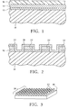
- Fig. 1 is a side sectional view of an embodiment of piezoelectric substrate having various layers formed on an upper surface.
- Fig. 2 is a side sectional view of the piezoelectric substrate of Fig. 1 having a patterned matching layer.
- Fig. 3 is a perspective view of the substrate of Fig. 2.
- Figs. 4 - 6 are top views of alternative embodiments of substrate.
- a piezoelectric substrate 10 is shown as having a number of layers formed atop the substrate.
- the piezoelectric substrate is a conventional piezoelectric material.
- An acceptable material for forming the piezoelectric substrate 10 is lead zirconate titanate (PZT).
- PZT lead zirconate titanate
- the thickness of the piezoelectric layer determines the operating frequency of the transducer.
- the "transducer” is the structure that converts an electrical excitation signal into acoustic waves and/or converts acoustic waves into an electrical signal.
- the design of the piezoelectric substrate 10 is not critical.
- the structure shown in Fig. 1 may be one element of a two-dimensional array of piezoelectric elements of a device used in medical imaging.
- the upper surface of the piezoelectric substrate 10 is a radiating surface for transmitting acoustic waves into a medium of interest.
- a nominal layer 12 is deposited on the radiating surface. The nominal layer is selected for its conductive and adhesive properties.
- An acceptable layer 12 is a first film of chrome having a thickness of approximately 10 nm (100 ⁇ ) and a second film of gold having a thickness of approximately 200 nm (2000 ⁇ ). While the surface of the piezoelectric substrate is shown as being planar, a spherically shaped transducer can also be used, since PZT is a porous material that will receive most of the nominal layer.
- a layer 14 of matching material is formed on the nominal layer 12. While not critical, the layer may be a high purity copper that is micro-electroplated onto the gold film of the nominal layer.
- the thickness of the matching layer is preferably one-quarter wavelength of the operating frequency of the piezoelectric transducer.
- a photoresist 16 is then deposited on the layer of matching material 14.
- the photoresist may be a conventional photo-negative resist. Standard techniques are employed to transfer a desired matching layer geometry to the photoresist.
- a mask may be positioned to selectively expose portions of the photoresist to ultraviolet radiation.
- the photoresist is developed and an etchant is used to remove portions of the photoresist 16 and the layer 14 of matching material.
- the etchant may or may not be selective to etching the nominal layer 12 as well, but should not readily etch the piezoelectric substrate 10.
- the nominal layer 12 is etched and an electrode layer 18 is then blanket deposited onto the patterned structure.
- a second electrode layer is formed on the back surface of the piezoelectric substrate.
- a source of an excitation signal is connected to the two electrode layers to transmit and receive electrical signals to and from the substrate.
- the patterned matching layer is shown as an array 20 of cylindrical posts 22. While not critical, the posts preferably have a thickness of one-quarter wavelength of the operating frequency of the transducer.
- the design of the cylindrical posts is dependent upon the media that is to be matched.
- the volume fraction of the filler material between the posts relative to the total volume of the posts and the spacing between the posts determines the acoustic impedance of the matching layer. In the above-cited reference of W.A. Smith in SPIE , Volume 1733 (1992), it is shown that by removing piezoelectric material from a bulk piezoelectric ceramic, the acoustic impedance of the bulk piezoelectric ceramic can be decreased with changes to the volume fraction of the remaining ceramic.
- the bulk velocity of PZT-5 drops to approximately 80% of its original value for a 30% volume fraction of remaining PZT-5.
- the optimal thickness of the matching layer for a piezoelectric transducer having a central frequency of 10 MHz is therefore 4032/(4 x 10 x 106), i.e. approximately 0.1 mm.
- the integration may also occur with lithium niobate, zinc oxide, a copolymer vinylidene fluoride with tetrafluorothylene P(VDF-TrFE), and crystalline quartz transducers.
- the techniques can be implemented directly by etching the desired matching layer pattern to a quarter-wavelength depth using integrated circuit techniques.
- a lead metaniobate transducer having an acoustic impedance of approximately 17 MRayls has a radiating surface on which an aluminum matching layer is patterned.
- a bulk aluminum matching layer has an impedance of approximately 17 MRayls and a bulk velocity of 6400 m/s.
- An improved impedance match to water may be obtained by patterning the bulk matching layer in a manner to provide an acoustic impedance of approximately 5.0 MRayls. This can be achieved with a low volume fraction of approximately 5% of aluminum.
- at 5% the velocity through the patterned matching layer is approximately 60% of the bulk velocity of aluminum. That is, the velocity is approximately 3840 m/s.
- the build-up to this thickness can be achieved by anodizing the face of the substrate.
- x-cut quartz may be used.
- the bulk velocity is 5740 m/s and the bulk acoustic impedance is 15.2 MRayls.
- An impedance match to water may be achieved by forming a segmented surface.
- the thickness of the matching layer will then be approximately 8.6 ⁇ m (0.34 mils).
- Another application would be one in which the copolymer vinylidene fluoride with tetrafluoroethylene P(VDF-TrFE) is to be used to transmit pulses into water.
- the bulk velocity of the copolymer is 2400 m/s and the acoustic impedance is 4.5 MRayls.
- the radiating surface onto which the array 20 of posts 22 is formed is the rear surface of the piezoelectric substrate 10 of Fig. 3. That is, rather than patterning the matching layer for efficient acoustic transmission to and from a medium of interest, the matching layer can be designed for efficient transmission of acoustic energy into a backing medium for absorbing acoustic energy.
- cylindrical posts 22 are shown as a single patterned layer, optionally impedance matching is achieved by forming successive films of different materials.
- the segmented matching layer 20 of Fig. 3 may be obtained by silkscreening an electrically conductive paste onto a piezoelectric substrate, such as one made of PZT-4 or PZT-5H.
- a metallic layer is applied to the piezoelectric substrate prior to the silkscreening process.
- a second metallization is formed.
- a preferred metallization is a nominal coating of chrome-gold.
- Injection molding is another alternative, but in the same manner as silkscreening, injection molding is limited to fabricating transducers to be operated at low frequencies.
- a matching layer having a graded impedance that more closely matches the impedance of the piezoelectric transducer at one side and the impedance of the medium of interest at the opposite side may be formed. This can be accomplished by having a volume fraction of a high impedance material gradually decline with departure from the transducer and approach to the medium. For example, conical projections or pyramids can be formed.
- the spaces between adjacent posts 22 may optionally be filled with a material such as epoxy.
- the epoxy fill does not affect the volume fraction of the matching material, but does add support for the posts.
- a matching layer having a configuration of a distribution of elliptical posts 24 is shown.
- the elliptical posts are formed on a piezoelectric substrate 26, such as PZT.
- the matching material may be copper and a chrome-gold metallization is preferably included.
- the elliptical posts are asymmetrical in the basal plane of the piezoelectric substrate 26. While forming a matching layer of this type is problematic, such formations provide advantages to tailoring acoustic impedance and controlling the lateral modes of vibration.
- FIG. 5 another distribution for a high volume fraction matching layer is shown.
- the distribution of four-sided posts 28 on a piezoelectric substrate 30 is one in which the posts vary in pitch with distance from the center of the substrate.
- the distribution may be Gaussian in the direction parallel to the longer substrate sides and half cosine in the direction parallel to the shorter sides of the substrate.
- An advantage of the embodiment of Fig. 5 is that the spatial difference of impedance matching achieved by varying the volume fraction of the matching material allows a greater center intensity of acoustic waves launched from the piezoelectric substrate. However, some spatial resolution is sacrificed.
- the matching layer includes an array of circular segments 32 on a piezoelectric substrate 34.
- the segments Preferably, the segments have a prescribed variation in the radial direction.
- the wave coupling is assumed to be maximal at a solid center segment 36 of the ultrasonic device. The coupling is then reduced with approach to an outer periphery.
Landscapes
- Physics & Mathematics (AREA)
- Engineering & Computer Science (AREA)
- Acoustics & Sound (AREA)
- Multimedia (AREA)
- Transducers For Ultrasonic Waves (AREA)
Applications Claiming Priority (2)
| Application Number | Priority Date | Filing Date | Title |
|---|---|---|---|
| US225127 | 1994-04-08 | ||
| US08/225,127 US5511296A (en) | 1994-04-08 | 1994-04-08 | Method for making integrated matching layer for ultrasonic transducers |
Publications (2)
| Publication Number | Publication Date |
|---|---|
| EP0676742A2 true EP0676742A2 (fr) | 1995-10-11 |
| EP0676742A3 EP0676742A3 (fr) | 1996-07-31 |
Family
ID=22843648
Family Applications (1)
| Application Number | Title | Priority Date | Filing Date |
|---|---|---|---|
| EP95302247A Withdrawn EP0676742A3 (fr) | 1994-04-08 | 1995-04-04 | Couche integré d'adaptation pour un transducteur ultrasonne. |
Country Status (3)
| Country | Link |
|---|---|
| US (1) | US5511296A (fr) |
| EP (1) | EP0676742A3 (fr) |
| JP (1) | JPH07298398A (fr) |
Cited By (2)
| Publication number | Priority date | Publication date | Assignee | Title |
|---|---|---|---|---|
| WO2009079467A2 (fr) * | 2007-12-18 | 2009-06-25 | Boston Scientific Scimed, Inc. | Matériaux composites passifs pour transducteurs d'ultrasons |
| WO2009085994A3 (fr) * | 2007-12-27 | 2010-07-01 | Boston Scientific Scimed, Inc. | Connexions pour transducteurs ultrasonores |
Families Citing this family (68)
| Publication number | Priority date | Publication date | Assignee | Title |
|---|---|---|---|---|
| US5883457A (en) * | 1997-04-24 | 1999-03-16 | Raychem Corporation | Organic matrix for acoustic reflector array |
| US5888577A (en) * | 1997-06-30 | 1999-03-30 | Procath Corporation | Method for forming an electrophysiology catheter |
| JP3926448B2 (ja) * | 1997-12-01 | 2007-06-06 | 株式会社日立メディコ | 超音波探触子及びこれを用いた超音波診断装置 |
| US6036647A (en) * | 1998-07-31 | 2000-03-14 | Scimed Life Systems, Inc. | PZT off-aperture bonding technique |
| US6019727A (en) * | 1998-07-31 | 2000-02-01 | Scimed Life Systems, Inc. | Center conductor and PZT bonding technique |
| US6036648A (en) * | 1998-10-23 | 2000-03-14 | Scimed Life Systems, Inc. | Machine tilt transducer and methods of making |
| US6835178B1 (en) * | 1999-06-23 | 2004-12-28 | Hologic, Inc. | Ultrasonic bone testing with copolymer transducers |
| JP4519330B2 (ja) * | 2001-01-11 | 2010-08-04 | パナソニック株式会社 | 超音波探触子 |
| US6666295B2 (en) * | 2001-01-23 | 2003-12-23 | Etymotic Research, Inc. | Acoustic resistor for hearing improvement and audiometric applications, and method of making same |
| US6758094B2 (en) * | 2001-07-31 | 2004-07-06 | Koninklijke Philips Electronics, N.V. | Ultrasonic transducer wafer having variable acoustic impedance |
| US20060028099A1 (en) * | 2004-08-05 | 2006-02-09 | Frey Gregg W | Composite acoustic matching layer |
| US10864385B2 (en) | 2004-09-24 | 2020-12-15 | Guided Therapy Systems, Llc | Rejuvenating skin by heating tissue for cosmetic treatment of the face and body |
| US8535228B2 (en) | 2004-10-06 | 2013-09-17 | Guided Therapy Systems, Llc | Method and system for noninvasive face lifts and deep tissue tightening |
| US8444562B2 (en) | 2004-10-06 | 2013-05-21 | Guided Therapy Systems, Llc | System and method for treating muscle, tendon, ligament and cartilage tissue |
| US9694212B2 (en) | 2004-10-06 | 2017-07-04 | Guided Therapy Systems, Llc | Method and system for ultrasound treatment of skin |
| US8133180B2 (en) | 2004-10-06 | 2012-03-13 | Guided Therapy Systems, L.L.C. | Method and system for treating cellulite |
| EP2409729A1 (fr) | 2004-10-06 | 2012-01-25 | Guided Therapy Systems, L.L.C. | Système et procédé pour le traitement de tissus par ultrasons |
| US20060111744A1 (en) | 2004-10-13 | 2006-05-25 | Guided Therapy Systems, L.L.C. | Method and system for treatment of sweat glands |
| US11235179B2 (en) | 2004-10-06 | 2022-02-01 | Guided Therapy Systems, Llc | Energy based skin gland treatment |
| CA2583600A1 (fr) | 2004-10-06 | 2006-04-20 | Guided Therapy Systems, L.L.C. | Methode et systeme de chirurgie esthetique non invasif |
| US9827449B2 (en) | 2004-10-06 | 2017-11-28 | Guided Therapy Systems, L.L.C. | Systems for treating skin laxity |
| US11883688B2 (en) | 2004-10-06 | 2024-01-30 | Guided Therapy Systems, Llc | Energy based fat reduction |
| US8690778B2 (en) | 2004-10-06 | 2014-04-08 | Guided Therapy Systems, Llc | Energy-based tissue tightening |
| US11724133B2 (en) | 2004-10-07 | 2023-08-15 | Guided Therapy Systems, Llc | Ultrasound probe for treatment of skin |
| US11207548B2 (en) | 2004-10-07 | 2021-12-28 | Guided Therapy Systems, L.L.C. | Ultrasound probe for treating skin laxity |
| KR100887226B1 (ko) * | 2007-09-19 | 2009-03-06 | 세메스 주식회사 | 초음파 진동 생성 장치 및 방법 그리고 웨이퍼 세정 장치및 방법 |
| JP4965485B2 (ja) * | 2008-02-29 | 2012-07-04 | 東京応化工業株式会社 | 処理液浸透ユニットおよび処理装置 |
| HUE027536T2 (en) | 2008-06-06 | 2016-10-28 | Ulthera Inc | Cosmetic treatment and imaging system |
| US12102473B2 (en) | 2008-06-06 | 2024-10-01 | Ulthera, Inc. | Systems for ultrasound treatment |
| WO2010075547A2 (fr) | 2008-12-24 | 2010-07-01 | Guided Therapy Systems, Llc | Procédés et systèmes pour réduire les graisses et/ou traiter la cellulite |
| JP5552820B2 (ja) * | 2010-01-28 | 2014-07-16 | コニカミノルタ株式会社 | 超音波探触子および超音波診断装置 |
| US8611567B2 (en) * | 2011-10-06 | 2013-12-17 | General Electric Company | Direct writing of functionalized acoustic backing |
| JP5574051B2 (ja) * | 2011-11-28 | 2014-08-20 | 株式会社村田製作所 | 積層型圧電素子、および、重送検知用センサ |
| US9510802B2 (en) | 2012-09-21 | 2016-12-06 | Guided Therapy Systems, Llc | Reflective ultrasound technology for dermatological treatments |
| CN113648552A (zh) | 2013-03-08 | 2021-11-16 | 奥赛拉公司 | 用于多焦点超声治疗的装置和方法 |
| GB2513884B (en) | 2013-05-08 | 2015-06-17 | Univ Bristol | Method and apparatus for producing an acoustic field |
| US9612658B2 (en) | 2014-01-07 | 2017-04-04 | Ultrahaptics Ip Ltd | Method and apparatus for providing tactile sensations |
| CN106470735B (zh) | 2014-04-18 | 2019-09-20 | 奥赛拉公司 | 带式换能器超声治疗 |
| GB2530036A (en) | 2014-09-09 | 2016-03-16 | Ultrahaptics Ltd | Method and apparatus for modulating haptic feedback |
| ES2896875T3 (es) | 2015-02-20 | 2022-02-28 | Ultrahaptics Ip Ltd | Percepciones en un sistema háptico |
| CA2976319C (fr) | 2015-02-20 | 2023-06-27 | Ultrahaptics Ip Limited | Ameliorations d'algorithme dans un systeme haptique |
| US10818162B2 (en) | 2015-07-16 | 2020-10-27 | Ultrahaptics Ip Ltd | Calibration techniques in haptic systems |
| US11189140B2 (en) | 2016-01-05 | 2021-11-30 | Ultrahaptics Ip Ltd | Calibration and detection techniques in haptic systems |
| AU2017208980B2 (en) | 2016-01-18 | 2022-03-31 | Ulthera, Inc. | Compact ultrasound device having annular ultrasound array peripherally electrically connected to flexible printed circuit board and method of assembly thereof |
| US10531212B2 (en) | 2016-06-17 | 2020-01-07 | Ultrahaptics Ip Ltd. | Acoustic transducers in haptic systems |
| US10268275B2 (en) | 2016-08-03 | 2019-04-23 | Ultrahaptics Ip Ltd | Three-dimensional perceptions in haptic systems |
| US10755538B2 (en) | 2016-08-09 | 2020-08-25 | Ultrahaptics ilP LTD | Metamaterials and acoustic lenses in haptic systems |
| SG11201809850QA (en) | 2016-08-16 | 2018-12-28 | Ulthera Inc | Systems and methods for cosmetic ultrasound treatment of skin |
| US10943578B2 (en) | 2016-12-13 | 2021-03-09 | Ultrahaptics Ip Ltd | Driving techniques for phased-array systems |
| US10497358B2 (en) | 2016-12-23 | 2019-12-03 | Ultrahaptics Ip Ltd | Transducer driver |
| CN108400231A (zh) * | 2017-02-08 | 2018-08-14 | 南昌欧菲生物识别技术有限公司 | 超声波传感器及超声波传感器的制造方法 |
| US11531395B2 (en) | 2017-11-26 | 2022-12-20 | Ultrahaptics Ip Ltd | Haptic effects from focused acoustic fields |
| US11704983B2 (en) | 2017-12-22 | 2023-07-18 | Ultrahaptics Ip Ltd | Minimizing unwanted responses in haptic systems |
| WO2019122912A1 (fr) | 2017-12-22 | 2019-06-27 | Ultrahaptics Limited | Suivi dans des systèmes haptiques |
| TWI797235B (zh) | 2018-01-26 | 2023-04-01 | 美商奧賽拉公司 | 用於多個維度中的同時多聚焦超音治療的系統和方法 |
| US11944849B2 (en) | 2018-02-20 | 2024-04-02 | Ulthera, Inc. | Systems and methods for combined cosmetic treatment of cellulite with ultrasound |
| KR20210002703A (ko) | 2018-05-02 | 2021-01-08 | 울트라햅틱스 아이피 엘티디 | 개선된 음향 전송 효율을 위한 차단 플레이트 구조체 |
| DE102018206937A1 (de) * | 2018-05-04 | 2019-11-07 | Fraunhofer-Gesellschaft zur Förderung der angewandten Forschung e.V. | Impedanzanpassungsvorrichtung, Wandlervorrichtung und Verfahren zum Herstellen einer Impedanzanpassungsvorrichtiung |
| US11098951B2 (en) | 2018-09-09 | 2021-08-24 | Ultrahaptics Ip Ltd | Ultrasonic-assisted liquid manipulation |
| US11378997B2 (en) | 2018-10-12 | 2022-07-05 | Ultrahaptics Ip Ltd | Variable phase and frequency pulse-width modulation technique |
| EP3906462A2 (fr) | 2019-01-04 | 2021-11-10 | Ultrahaptics IP Ltd | Textures haptiques aériennes |
| US11842517B2 (en) | 2019-04-12 | 2023-12-12 | Ultrahaptics Ip Ltd | Using iterative 3D-model fitting for domain adaptation of a hand-pose-estimation neural network |
| AU2020368678A1 (en) | 2019-10-13 | 2022-05-19 | Ultraleap Limited | Dynamic capping with virtual microphones |
| US11374586B2 (en) | 2019-10-13 | 2022-06-28 | Ultraleap Limited | Reducing harmonic distortion by dithering |
| US11169610B2 (en) | 2019-11-08 | 2021-11-09 | Ultraleap Limited | Tracking techniques in haptic systems |
| US11715453B2 (en) | 2019-12-25 | 2023-08-01 | Ultraleap Limited | Acoustic transducer structures |
| US11816267B2 (en) | 2020-06-23 | 2023-11-14 | Ultraleap Limited | Features of airborne ultrasonic fields |
| WO2022058738A1 (fr) | 2020-09-17 | 2022-03-24 | Ultraleap Limited | Ultrahapticons |
Citations (5)
| Publication number | Priority date | Publication date | Assignee | Title |
|---|---|---|---|---|
| FR2546306A1 (fr) * | 1983-05-20 | 1984-11-23 | Labo Electronique Physique | Appareil d'examen echographique de milieux aux ultrasons equipe d'un nouveau type de dispositif de transduction ultrasonore |
| US4507582A (en) * | 1982-09-29 | 1985-03-26 | New York Institute Of Technology | Matching region for damped piezoelectric ultrasonic apparatus |
| JPS60135858A (ja) * | 1983-12-26 | 1985-07-19 | Toshiba Corp | 超音波探触子及びその製造方法 |
| US4756808A (en) * | 1985-05-31 | 1988-07-12 | Nec Corporation | Piezoelectric transducer and process for preparation thereof |
| EP0629994A2 (fr) * | 1993-06-15 | 1994-12-21 | Hewlett-Packard Company | Microrainures pour la conception des transducteurs cliniques ultrasonores à large bande |
Family Cites Families (2)
| Publication number | Priority date | Publication date | Assignee | Title |
|---|---|---|---|---|
| US4939826A (en) * | 1988-03-04 | 1990-07-10 | Hewlett-Packard Company | Ultrasonic transducer arrays and methods for the fabrication thereof |
| US5327895A (en) * | 1991-07-10 | 1994-07-12 | Kabushiki Kaisha Toshiba | Ultrasonic probe and ultrasonic diagnosing system using ultrasonic probe |
-
1994
- 1994-04-08 US US08/225,127 patent/US5511296A/en not_active Expired - Fee Related
-
1995
- 1995-04-04 EP EP95302247A patent/EP0676742A3/fr not_active Withdrawn
- 1995-04-07 JP JP7108139A patent/JPH07298398A/ja active Pending
Patent Citations (5)
| Publication number | Priority date | Publication date | Assignee | Title |
|---|---|---|---|---|
| US4507582A (en) * | 1982-09-29 | 1985-03-26 | New York Institute Of Technology | Matching region for damped piezoelectric ultrasonic apparatus |
| FR2546306A1 (fr) * | 1983-05-20 | 1984-11-23 | Labo Electronique Physique | Appareil d'examen echographique de milieux aux ultrasons equipe d'un nouveau type de dispositif de transduction ultrasonore |
| JPS60135858A (ja) * | 1983-12-26 | 1985-07-19 | Toshiba Corp | 超音波探触子及びその製造方法 |
| US4756808A (en) * | 1985-05-31 | 1988-07-12 | Nec Corporation | Piezoelectric transducer and process for preparation thereof |
| EP0629994A2 (fr) * | 1993-06-15 | 1994-12-21 | Hewlett-Packard Company | Microrainures pour la conception des transducteurs cliniques ultrasonores à large bande |
Non-Patent Citations (2)
| Title |
|---|
| PATENT ABSTRACTS OF JAPAN vol. 009, no. 299 (P-408), 27 November 1985 & JP-A-60 135858 (TOSHIBA KK), 19 July 1985, * |
| PROCEEDINGS OF THE ULTRASONICS SYMPOSIUM, LAKE BUENA VISTA, DEC. 8 - 11, 1991, vol. 1, 8 December 1991, MCAVOY B R, pages 403-405, XP000347180 HALLER M I ET AL: "MICROMACHINED ULTRASONIC MATERIALS" * |
Cited By (5)
| Publication number | Priority date | Publication date | Assignee | Title |
|---|---|---|---|---|
| WO2009079467A2 (fr) * | 2007-12-18 | 2009-06-25 | Boston Scientific Scimed, Inc. | Matériaux composites passifs pour transducteurs d'ultrasons |
| WO2009079467A3 (fr) * | 2007-12-18 | 2010-04-22 | Boston Scientific Scimed, Inc. | Matériaux composites passifs pour transducteurs d'ultrasons |
| US7804228B2 (en) | 2007-12-18 | 2010-09-28 | Boston Scientific Scimed, Inc. | Composite passive materials for ultrasound transducers |
| WO2009085994A3 (fr) * | 2007-12-27 | 2010-07-01 | Boston Scientific Scimed, Inc. | Connexions pour transducteurs ultrasonores |
| US8390174B2 (en) | 2007-12-27 | 2013-03-05 | Boston Scientific Scimed, Inc. | Connections for ultrasound transducers |
Also Published As
| Publication number | Publication date |
|---|---|
| EP0676742A3 (fr) | 1996-07-31 |
| JPH07298398A (ja) | 1995-11-10 |
| US5511296A (en) | 1996-04-30 |
Similar Documents
| Publication | Publication Date | Title |
|---|---|---|
| US5511296A (en) | Method for making integrated matching layer for ultrasonic transducers | |
| US5553035A (en) | Method of forming integral transducer and impedance matching layers | |
| US5792058A (en) | Broadband phased array transducer with wide bandwidth, high sensitivity and reduced cross-talk and method for manufacture thereof | |
| EP3121844B1 (fr) | Transducteurs à ultrasons | |
| CN100398224C (zh) | 换能器的频率和振幅旁瓣缩减 | |
| US4385255A (en) | Linear array ultrasonic transducer | |
| JP3950755B2 (ja) | イメージング・システムの分解能を高める超音波トランスデューサ | |
| EP0629994B1 (fr) | Microrainures pour la conception des transducteurs cliniques ultrasonores à large bande | |
| US6974417B2 (en) | Ultrasound transducer array | |
| US6761692B2 (en) | High frequency and multi frequency band ultrasound transducers based on ceramic films | |
| AU679035B2 (en) | Ultrasound transducers with reduced sidelobes and method for manufacture thereof | |
| US5434827A (en) | Matching layer for front acoustic impedance matching of clinical ultrasonic tranducers | |
| EP0142215A2 (fr) | Transducteur ultrasonore ayant des modes vibratoires améliorées | |
| CN111465455B (zh) | 高频超声波换能器 | |
| JP3824315B2 (ja) | 多次元アレイとその製造 | |
| US5371717A (en) | Microgrooves for apodization and focussing of wideband clinical ultrasonic transducers | |
| JP2004511290A (ja) | 脈管内超音波カテーテル配置 | |
| US5511550A (en) | Ultrasonic transducer array with apodized elevation focus | |
| US6036647A (en) | PZT off-aperture bonding technique | |
| JPH07322393A (ja) | 超音波探触子 | |
| Seyed-Bolorforosh | Novel integrated impedance matching layer | |
| JPS62208800A (ja) | 超音波探触子 |
Legal Events
| Date | Code | Title | Description |
|---|---|---|---|
| PUAI | Public reference made under article 153(3) epc to a published international application that has entered the european phase |
Free format text: ORIGINAL CODE: 0009012 |
|
| AK | Designated contracting states |
Kind code of ref document: A2 Designated state(s): DE FR GB NL |
|
| PUAL | Search report despatched |
Free format text: ORIGINAL CODE: 0009013 |
|
| AK | Designated contracting states |
Kind code of ref document: A3 Designated state(s): DE FR GB NL |
|
| 17P | Request for examination filed |
Effective date: 19961230 |
|
| STAA | Information on the status of an ep patent application or granted ep patent |
Free format text: STATUS: THE APPLICATION HAS BEEN WITHDRAWN |
|
| 18W | Application withdrawn |
Withdrawal date: 19981116 |