EP0670570A2 - Magnetoresistiver Kopf und Herstellungsverfahren - Google Patents
Magnetoresistiver Kopf und Herstellungsverfahren Download PDFInfo
- Publication number
- EP0670570A2 EP0670570A2 EP95301317A EP95301317A EP0670570A2 EP 0670570 A2 EP0670570 A2 EP 0670570A2 EP 95301317 A EP95301317 A EP 95301317A EP 95301317 A EP95301317 A EP 95301317A EP 0670570 A2 EP0670570 A2 EP 0670570A2
- Authority
- EP
- European Patent Office
- Prior art keywords
- pole
- gap
- head
- magnetoresistive head
- reader
- Prior art date
- Legal status (The legal status is an assumption and is not a legal conclusion. Google has not performed a legal analysis and makes no representation as to the accuracy of the status listed.)
- Granted
Links
Images


Classifications
-
- G—PHYSICS
- G11—INFORMATION STORAGE
- G11B—INFORMATION STORAGE BASED ON RELATIVE MOVEMENT BETWEEN RECORD CARRIER AND TRANSDUCER
- G11B5/00—Recording by magnetisation or demagnetisation of a record carrier; Reproducing by magnetic means; Record carriers therefor
- G11B5/127—Structure or manufacture of heads, e.g. inductive
- G11B5/33—Structure or manufacture of flux-sensitive heads, i.e. for reproduction only; Combination of such heads with means for recording or erasing only
- G11B5/39—Structure or manufacture of flux-sensitive heads, i.e. for reproduction only; Combination of such heads with means for recording or erasing only using magneto-resistive devices or effects
- G11B5/3903—Structure or manufacture of flux-sensitive heads, i.e. for reproduction only; Combination of such heads with means for recording or erasing only using magneto-resistive devices or effects using magnetic thin film layers or their effects, the films being part of integrated structures
- G11B5/3967—Composite structural arrangements of transducers, e.g. inductive write and magnetoresistive read
-
- G—PHYSICS
- G11—INFORMATION STORAGE
- G11B—INFORMATION STORAGE BASED ON RELATIVE MOVEMENT BETWEEN RECORD CARRIER AND TRANSDUCER
- G11B5/00—Recording by magnetisation or demagnetisation of a record carrier; Reproducing by magnetic means; Record carriers therefor
- G11B5/127—Structure or manufacture of heads, e.g. inductive
- G11B5/31—Structure or manufacture of heads, e.g. inductive using thin films
- G11B5/3163—Fabrication methods or processes specially adapted for a particular head structure, e.g. using base layers for electroplating, using functional layers for masking, using energy or particle beams for shaping the structure or modifying the properties of the basic layers
Definitions
- the present invention relates to a magnetoresistive head for reading information from and writing information to a recording medium, and to a method of manufacturing a magnetoresistive head.
- Standard magnetoresistive (MR) heads are fabricated with the writer portion fabricated on top of the reader portion.
- US Patent No. 4,803,580 discloses one such device.
- MR heads are used in magnetic storage systems to detect magnetically encoded information from a magnetic storage medium or disc and to write magnetically encoded information to the storage medium.
- a time dependent magnetic field associated with a transition from a magnetic storage medium directly modulates the resistivity of an MR element.
- the change in resistance of the MR element can be detected by passing a sense current through the MR element and measuring the voltage across the MR element. The resulting signal can be used to recover information or data from the magnetic storage medium.
- Magnetic MR elements are typically formed using ferromagnetic metal alloys because of their high magnetic permeability, an example of which is nickel iron (NiFe).
- NiFe nickel iron
- a ferromagnetic material is deposited in a thin film upon the surface of an electrically insulated substrate or wafer. Changing magnetic fields originating from the magnetic storage medium produce a change in the magnetization direction of the MR element and thereby change the resistance of the sensor. This phenomenon is called the MR effect.
- the element itself comprises a strip of MR material deposited on a magnetic shield layer to form an MR element.
- a series of depositions and etching processes form an active region from a portion of the MR element.
- the active region is the area of the MR element that senses changing magnetic fields from the magnetic storage medium.
- An upper magnetic shield acts as a barrier between the MR element and the surface of the magnetic storage medium to prevent changing magnetic fields associated with transitions passing by the head from linking back to the element.
- the magnetic shield also serves to protect the element from receiving stray magnetic fields associated with transitions from surrounding magnetic storage media.
- top shield of an MR sensor has a dip just above the active region of the MR element. This degrades off track performance. Lack of planarization can also cause an electrical short either between the contacts to the MR element and the top shield or between the top shield and subsequent fabricated layers.
- top surface of the bottom shield is usually coated with sendust, which is relatively rough for a thin film. This relatively rough surface can also cause shorting problems between the bottom shield and the contact film. Attempts at planarizing MR readers have focused on smoothing the bottom shield, planarizing the insulator above the MR sensor, or smoothing the top shield. These steps take additional process time and can limit design flexibility.
- a method of manufacturing an magnetoresistive head comprising: fabricating a bottom pole in a basecoat with a recessed portion above the bottom pole distal from an air bearing surface of the head; positioning a polymer insulator and conductive coils in the recessed portion above the bottom pole; planarizing a top surface of the polymer insulator positioned in the recessed portion; fabricating a write gap on top of the top surface of the polymer; forming a pole tip of non-magnetic high moment material in the write gap proximal to the air bearing surface; planarizing a top surface of the write gap; fabricating a top pole/bottom shield on top of the pole tip and the write gap; fabricating a first reader gap on top of the top pole/bottom shield; forming a magnetoresistive element on top of a portion of the first reader gap proximal to the air bearing surface; fabricating electrical contacts on top of a portion of the first reader gap, the contacts electrically connecting
- a magnetoresistive head for reading information from a storage medium and for writing information to the storage medium, the magnetoresistive head characterised by comprising: a bottom pole having a recessed portion positioned above the bottom pole distal from an air bearing surface of the head; a polymer insulator positioned in the recessed portion of the bottom pole having a plurality of coils spaced throughout the polymer insulator, the polymer insulator having a planarized top surface; a write gap positioned on top of the polymer insulator, the write gap having a planarized top surface; a pole tip positioned in the write gap proximal to the air bearing surface; a top pole/bottom shield positioned on top of a portion of the write gap and the pole tip; a first reader gap positioned on top of the top pole/bottom shield; a magnetoresistive element positioned on top of the first reader gap proximal to the air bearing surface; electrical contacts positioned on top of the magnetoresistive element connecting the
- a method of manufacturing a magnetoresistive head comprising forming a multi-layered write portion and forming a multi-layered read portion, characterised in that the read portion is formed on top of the write portion, and/or in that at least one layer of the head is planarized.
- the insulating layer of the write portion may be polymer or another insulating material.
- magnetoresistive heads of the present invention may be referred to as inverted magnetoresistive heads. This term is used in the following text.
- the present invention is an inverted magnetoresistive head and a method of manufacturing an inverted magnetoresistive head for reading magnetically stored information from a magnetic storage medium.
- the inverted magnetoresistive head may include a reader positioned on top of a writer.
- the writer may include a recessed bottom pole filled with coils and polymer insulators above the recessed portion above the bottom pole. This bottom pole and coil structure may then be planarized.
- a write gap oxide layer may be deposited on top of the planarized bottom pole/coil structure.
- a high moment material top pole tip may be formed and the remaining part of the top pole structure, which is also the bottom shield of the reader, may then be formed. This bottom shield may be planarized.
- the first reader gap oxide layer may be deposited on top of the planarized bottom shield.
- a magnetoresistive element may be formed on top of the first reader gap oxide layer. Contacts may connect the magnetoresistive element to a region outside the magnetoresistive head.
- a second reader gap may be positioned on top of the magnetoresistive element and the contacts.
- a top shield may be positioned on top of the second reader gap.
- Figure 1A is a cross-sectional view of the layer structure of a prior art magnetoresistive head.
- Figure 1B is a cross-sectional view showing the layer structure of the air bearing surface of a prior art magnetoresistive head.
- Figure 2 is a cross-sectional view of the layer structure of a bottom pole of a writer of a magnetoresistive head prior to planarization.
- Figure 3 is a cross-sectional view of the layer structure of a bottom pole of a writer of a magnetoresistive head after planarization.
- Figure 4 is a cross-sectional view of the layer structure of a bottom portion of a writer showing a recessed channel in the write gap.
- Figure 5 is a cross-sectional view of the layer structure of a writer of a magnetoresistive head.
- Figure 6 is a cross-sectional view showing the layer of the air bearing surface of a writer of a magnetoresistive head.
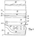
- Figure 7 is a cross-sectional view of the layer structure of a complete magnetoresistive head.
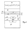
- Figure 8 is a cross-sectional view showing the layer structure of the air bearing surface of a complete magnetoresistive head.
- FIG 1A is a cross-sectional view of the layer structure of the prior art magnetoresistive (MR) head 10.
- MR head 10 of Figure 1 is a standard MR head having the writer portion of the head positioned on top of the reader portion of the head.
- MR head 10 includes basecoat oxide 12, bottom shield 14, first reader gap oxide layer 16, electrical contacts 18, MR element 20, second reader gap oxide layer 22, top shield/bottom pole 24, write gap oxide layer 26, polymer insulator layers 28a, 28b, and 28c, conductive coil layers 30a and 30b, and top pole 32.
- Bottom shield 14 is deposited upon basecoat oxide 12.
- First read gap oxide layer 16 is then deposited upon bottom shield 14.
- MR element 20 is deposited in a magnetic field and patterned.
- MR element 20 is the portion of MR head 10 which senses a magnetic field associated with a transition from a magnetic storage medium during a read operation.
- Electrical contacts 18 are then deposited on MR element 20 and first read gap oxide layer 16.
- Second read gap oxide layer 22 is then deposited.
- the two oxide layers, 16 and 22, comprise the read gaps, inside which MR element 20 is fabricated.
- top shield/bottom pole 24 is laid down. Top shield/bottom pole 24 is normally utilized to provide the top shield of the reader portion of MR head 10 as well as the bottom pole of the writer portion of MR head 10.
- Write gap oxide layer 26 is deposited, followed by polymer insulator layer 28a, conductive coil layer 30a, polymer insulator layer 28b, conductive coil layer 30b, and polymer insulator layer 28c. Finally, top pole 32 is deposited to complete the fabrication of MR head 10. Top shield/bottom pole 24 and top pole 32 provide the writing capability of MR head 10 during a write operation.
- the number of conductive coils 30 and polymer insulator layers 28 are determined by design and affect the inductance capabilities of the writer portion of MR head 10. Each polymer insulator layer, however, must be cured at temperatures between 200°C and 400°C for varying lengths of time depending upon the specific polymer. Only the lower half of this temperature range for the curing process will avoid possible degradation of the magnetics of the reader portion of MR head 10. This limits the choice of polymers available as insulators for MR head readers.
- FIG. 1B is a cross-sectional view showing the layer structure of the air bearing surface of the MR head.
- MR head 10 is fabricated such that a top surface of second read gap oxide layer 22 is not flat or planarized.
- the non-planar surface of second read gap oxide layer 22 dictates that subsequent deposited layers of MR head 10 are also not flat or planarized.
- top pole 32 which is covered by overcoat oxide layer 33, can be offset from the center of MR head 10, which can degrade the quality of tracks written from MR head 10.
- it is desired that each deposited layer of MR head 10 is flat or planarized to prevent shorting of later deposited layers, thereby rendering MR head 10 inoperable.
- Figure 2 is a cross-sectional view showing the layer structure near air bearing surface 52 of bottom pole 56 according to an embodiment of the present invention.
- Inverted MR head 50 includes base coat 54, bottom pole 56, polymer insulator 58 having top surface 60 and dip 62, and conductive coils 64.
- Leading edge 51 is identified relative to air bearing surface 52.
- bottom pole 56 formed from plated permalloy, is initially deposited into a recessed portion of basecoat 54.
- the recess in basecoat 54 is formed through a combination of chemical etching and ion milling.
- Polymer insulator 58 and conductive coils 64 fill the recessed portion above bottom pole 56.
- Conductive coils 64 which are typically made of copper, can be positioned in polymer insulator 58 in one row, or as seen in Figure 2, conductive coils 64 can be positioned in a plurality of rows. The number of conductive coils 64 and polymer insulator layers 58 affects the inductance capabilities of the writer portion of inverted MR head 50.
- top surface 60 of polymer insulator 58 can be somewhat irregular. Dip 62 can arise due to loss of polymer volume during the curing process.
- the top surface 60 of polymer insulator 58 is made flat or planarized so that the remaining layers of inverted MR head 50 which are deposited on top of top surface 60 are deposited on a flat surface. Thus, any rough, jagged portions of top surface 60, including dip 62, should be eliminated.
- top surface 60 As shown in Figure 3, all jagged and rough portions of top surface 60, including dip 62, have been eliminated. This elimination is normally done in one of two ways. First, the polymer material forming polymer insulator 58 can be deposited such that top surface 60 is higher than bottom pole 56. Top surface 60 can then undergo both a blanket reactive ion etch-back process and/or a chemical-mechanical polish until top surface 60 of polymer insulator 58 is both smooth and level with bottom pole 56. Second, the polymer material forming polymer insulator 58 can be deposited having rough top surface 60 and dip 62 (shown in Figure 2). A layer of silica can be deposited such that the top surface of the silica layer is slightly above bottom pole 56.
- photoresist is deposited on top of the silica layer.
- the photoresist and silica layer can then undergo a blanket reactive ion etch-back process that removes the silica and photoresist at the same rate, until top surface 60 of polymer insulator 58 is both smooth and entirely flat.
- inverted MR head 50 further includes write gap oxide layer 66 having top surface 68 and channel 70.
- Write gap oxide layer 66 is deposited on top of top surface 60 of polymer insulator 58.
- Write gap oxide layer 66 can be formed from a variety of insulating materials, such as silica, alumina, or diamond-like carbon.
- Channel 70, located near air-bearing surface 52, is then ion-milled into write gap oxide layer 66 to define actual write gap 66a beneath channel 70. This allows extremely accurate definition of the pole tip 72 (shown in Figures 5 and 6). The reason is that the photoresist is deposited upon a flat surface, allowing more precise development of the features in the photoresist mask.
- Write gap oxide layer 66a at air bearing surface 52 beneath channel 70 has a height in the range of approximately 0.1 microns to 1.0 microns, and preferably in the range of approximately 0.2 to 0.8 microns.
- pole tip 72 is positioned at trailing edge 73 of air bearing surface 52 of inverted MR head 50.
- Pole tip 72 is an insert formed from a high moment magnetic material such as iron nitride or cobalt iron.
- a high moment magnetic material is capable of supporting a larger density flux than the permalloy used in standard MR heads.
- the high moment insert forming pole tip 72 concentrates the magnetic flux and allows writing of a narrow track.
- the high momentum magnetic material forming pole tip 72 is either plated or sputtered into channel 70 until it is significantly higher than top surface 68 of write gap oxide layer 66.
- the thickness of the high moment insert depends upon the magnetic materials in the writer design. Typical values for the thickness of the insert range from 0.5 to 2.0 microns, and typical values for the track width of the pole tip range from 2.0 to 5.0 microns.
- a non-magnetic seed layer such as nickel vanadium (Ni80 V20) can be used, which then becomes part of the write gap.
- the protruding section of high moment material is then masked and permalloy is plated around it to obtain an approximately level surface.
- the masking above the insert is then removed and the entire shield is plated as a unit to the desired thickness.
- the top surface of the top pole 72/bottom shield 74 combination will very likely contain irregularities, which are then removed by chemical mechanical polishing.
- Figure 6 is a side cross-sectional view showing air bearing surface 52 of a writer of inverted MR head 50.
- pole tip 72 is aligned above bottom pole 56; with the critical portion of write gap oxide layer 66A located between bottom pole 56 and pole tip 72.
- the distance between bottom pole 56 and pole tip 72, which is the critical distance of write gap oxide layer 66 is in the range of approximately 1,000 to 10,000 angstroms, and preferably in the range of approximately 2,000 to 8,000 angstroms.
- bottom pole 56 has a height in the range of approximately 2.0 to 4.0 micrometers
- write gap oxide layer 66 formed between top surface 60 of polymer insulator 58 and top surface 68 has a height in the range of approximately 2,000 to 8,000 angstroms
- pole tip 72 has a height in the range of approximately 5,000 to 20,000 angstroms
- bottom shield 74 between top surface 68 of write gap oxide layer 66 and top surface 76 of bottom shield 74 has a height in the range of approximately 1.5 to 4.0 micrometers.
- Figure 7 is a cross-sectional view showing the entire fabricated inverted MR head 50, including both the writer and the reader portions of inverted MR head 50.
- first reader gap oxide layer 78 is deposited on top of bottom shield 74.
- first reader gap oxide layer 78 has a height of less than 4,000 Angstroms.
- MR element 80 is fabricated on first reader gap oxide layer 78 near trailing edge 73 of inverted MR head 50.
- MR element 80 may be a single film or composite film structure. The specific embodiment of MR element 80 does not affect the usefulness of MR head 50.
- Electrical contacts 82 are then deposited, followed by second reader gap oxide layer 84, top shield 86, and overcoat oxide layer 88.
- second reader gap oxide layer 84 has a height of less than 4, 000 Angstroms and the top shield 86 has a height in the range of approximately 1.5 to 4.0 micrometers.
- a boundary control stabilization layer, a permanent magnet stabilization layer, and/or an additional layer of contacts for inductive cancellation or low circuit resistance can be incorporated into the MR reader if necessary for a particular application.
- Figure 8 is an air bearing surface view of inverted MR head 50 showing both the reader and the writer.
- bottom pole 56, top pole 72, and MR element 80 are aligned with one another.
- This invention improves the accuracy of the alignment of the MR sensor to the top pole, since there are only one or two intervening mask layers to complicate mask alignment, as compared to ten or more intervening mask layers in prior art non-inverted MR heads.
- the alignment of bottom pole 56, top pole 72, and MR element 80 is critical in forming an MR head which can both precisely read information from a magnetic storage medium and write information to the magnetic storage medium.
- inverted MR head 50 of the described embodiment of the present invention there are several advantages of inverted MR head 50 of the described embodiment of the present invention.
- Third, planarity of the top pole 72 allows the reader and the writer to be offset without the top pole having a dip in it, such as the dip of the prior art shown in Figure 1B.
- use of sendust or other rough films for the top shield will not cause shorting due to roughness, since the only film above the top shield surface is the overcoat.
- Giant MR sensors have a structure consisting of layers of magnetic and layers of non-magnetic material, preferably ferromagnetic/non-ferromagnetic material or materials similar thereto. Permalloy may or may not be part of the layered pattern.
Landscapes
- Engineering & Computer Science (AREA)
- Manufacturing & Machinery (AREA)
- Magnetic Heads (AREA)
Applications Claiming Priority (2)
| Application Number | Priority Date | Filing Date | Title |
|---|---|---|---|
| US206007 | 1988-06-13 | ||
| US20600794A | 1994-03-03 | 1994-03-03 |
Publications (3)
| Publication Number | Publication Date |
|---|---|
| EP0670570A2 true EP0670570A2 (de) | 1995-09-06 |
| EP0670570A3 EP0670570A3 (de) | 1997-01-22 |
| EP0670570B1 EP0670570B1 (de) | 2000-04-26 |
Family
ID=22764596
Family Applications (1)
| Application Number | Title | Priority Date | Filing Date |
|---|---|---|---|
| EP19950301317 Expired - Lifetime EP0670570B1 (de) | 1994-03-03 | 1995-03-01 | Magnetoresistiver Kopf und Herstellungsverfahren |
Country Status (4)
| Country | Link |
|---|---|
| EP (1) | EP0670570B1 (de) |
| JP (1) | JPH07262535A (de) |
| DE (1) | DE69516442T2 (de) |
| HK (1) | HK1013354A1 (de) |
Cited By (8)
| Publication number | Priority date | Publication date | Assignee | Title |
|---|---|---|---|---|
| EP0747887A2 (de) * | 1995-06-07 | 1996-12-11 | Seagate Technology, Inc. | Herstellungsverfahren eines invertierten magnetoresistiven Kopfes |
| EP0752700A2 (de) * | 1995-07-05 | 1997-01-08 | Sony Corporation | Komplexer Dünnfilmmagnetkopf und Herstellungsverfahren |
| WO1998027545A1 (en) * | 1996-12-18 | 1998-06-25 | Koninklijke Philips Electronics N.V. | Method of manufacturing a layered magnetic head and a magnetic head |
| WO1998044487A2 (en) * | 1997-04-01 | 1998-10-08 | Koninklijke Philips Electronics N.V. | Method of manufacturing a magnetic head having a structure of layers |
| EP0894319A1 (de) * | 1996-04-18 | 1999-02-03 | Storage Technology Corporation | Dünnfilmmagnetkopf mit geringem spalt zwischen den polspitzen |
| US6259585B1 (en) | 1997-01-25 | 2001-07-10 | Tdk Corporation | Inverted hybrid thin film magnetic head and method of manufacturing the same |
| US7180706B2 (en) * | 2002-07-11 | 2007-02-20 | International Business Machines Corporation | Magnetic heads and semiconductor devices and surface planarization processes for the fabrication thereof |
| US10591679B2 (en) | 2014-12-01 | 2020-03-17 | Commscope Asia Holdings B.V. | Multi-fiber optic connector with pivotally-aligned ferrule using dual spring force ensuring pressed-together contact faces |
Families Citing this family (1)
| Publication number | Priority date | Publication date | Assignee | Title |
|---|---|---|---|---|
| SG115532A1 (en) * | 2002-04-03 | 2005-10-28 | Seagate Technology Llc | Perpendicular writer pole having a nonmagnetic seedlayer |
Citations (13)
| Publication number | Priority date | Publication date | Assignee | Title |
|---|---|---|---|---|
| JPS6050711A (ja) * | 1983-08-31 | 1985-03-20 | Hitachi Ltd | 薄膜磁気ヘツド |
| JPS60177420A (ja) * | 1984-02-23 | 1985-09-11 | Nec Corp | 複合型薄膜磁気ヘツド及びその製造方法 |
| JPS61120318A (ja) * | 1984-11-15 | 1986-06-07 | Matsushita Electric Ind Co Ltd | 一体化薄膜磁気ヘツド |
| JPH0196814A (ja) * | 1987-10-09 | 1989-04-14 | Hitachi Ltd | 複合型薄膜磁気ヘッド |
| JPH0291807A (ja) * | 1988-09-28 | 1990-03-30 | Sanyo Electric Co Ltd | 複合型薄膜磁気ヘッド |
| US5130877A (en) * | 1990-04-26 | 1992-07-14 | Seagate Technology, Inc. | Thin film head on ferrite substrate with inclined top pole |
| US5155646A (en) * | 1989-07-26 | 1992-10-13 | Victor Company Of Japan, Ltd. | Multiple layered thin-film magnetic head for magnetic recording and reproducing apparatus |
| EP0516022A2 (de) * | 1991-05-30 | 1992-12-02 | Matsushita Electric Industrial Co., Ltd. | Integrierter Dünnfilm-Magnetkopf |
| EP0519558A1 (de) * | 1991-06-18 | 1992-12-23 | Koninklijke Philips Electronics N.V. | Dünnfilm-Lese-/Schreibkopf ohne Pol-Umgreifeffekt |
| EP0548511A1 (de) * | 1991-12-18 | 1993-06-30 | Hewlett-Packard Company | Induktiver Dünnfilmwandler mit verbesserter Schreibfähigkeit |
| DE4312040A1 (de) * | 1992-04-13 | 1993-10-14 | Hitachi Ltd | Magnetisches Speicher-/Lesesystem |
| EP0574896A2 (de) * | 1992-06-17 | 1993-12-22 | Sony Corporation | Zusammengesetzter Dünnfilmmagnetkopf |
| EP0617409A2 (de) * | 1993-03-22 | 1994-09-28 | Koninklijke Philips Electronics N.V. | Herstellungsverfahren eines Dünnfilmmagnetkopfes und danach hergestellter Magnetkopf |
-
1995
- 1995-03-01 EP EP19950301317 patent/EP0670570B1/de not_active Expired - Lifetime
- 1995-03-01 DE DE1995616442 patent/DE69516442T2/de not_active Expired - Fee Related
- 1995-03-02 JP JP4292095A patent/JPH07262535A/ja active Pending
-
1998
- 1998-12-22 HK HK98114550A patent/HK1013354A1/xx not_active IP Right Cessation
Patent Citations (13)
| Publication number | Priority date | Publication date | Assignee | Title |
|---|---|---|---|---|
| JPS6050711A (ja) * | 1983-08-31 | 1985-03-20 | Hitachi Ltd | 薄膜磁気ヘツド |
| JPS60177420A (ja) * | 1984-02-23 | 1985-09-11 | Nec Corp | 複合型薄膜磁気ヘツド及びその製造方法 |
| JPS61120318A (ja) * | 1984-11-15 | 1986-06-07 | Matsushita Electric Ind Co Ltd | 一体化薄膜磁気ヘツド |
| JPH0196814A (ja) * | 1987-10-09 | 1989-04-14 | Hitachi Ltd | 複合型薄膜磁気ヘッド |
| JPH0291807A (ja) * | 1988-09-28 | 1990-03-30 | Sanyo Electric Co Ltd | 複合型薄膜磁気ヘッド |
| US5155646A (en) * | 1989-07-26 | 1992-10-13 | Victor Company Of Japan, Ltd. | Multiple layered thin-film magnetic head for magnetic recording and reproducing apparatus |
| US5130877A (en) * | 1990-04-26 | 1992-07-14 | Seagate Technology, Inc. | Thin film head on ferrite substrate with inclined top pole |
| EP0516022A2 (de) * | 1991-05-30 | 1992-12-02 | Matsushita Electric Industrial Co., Ltd. | Integrierter Dünnfilm-Magnetkopf |
| EP0519558A1 (de) * | 1991-06-18 | 1992-12-23 | Koninklijke Philips Electronics N.V. | Dünnfilm-Lese-/Schreibkopf ohne Pol-Umgreifeffekt |
| EP0548511A1 (de) * | 1991-12-18 | 1993-06-30 | Hewlett-Packard Company | Induktiver Dünnfilmwandler mit verbesserter Schreibfähigkeit |
| DE4312040A1 (de) * | 1992-04-13 | 1993-10-14 | Hitachi Ltd | Magnetisches Speicher-/Lesesystem |
| EP0574896A2 (de) * | 1992-06-17 | 1993-12-22 | Sony Corporation | Zusammengesetzter Dünnfilmmagnetkopf |
| EP0617409A2 (de) * | 1993-03-22 | 1994-09-28 | Koninklijke Philips Electronics N.V. | Herstellungsverfahren eines Dünnfilmmagnetkopfes und danach hergestellter Magnetkopf |
Non-Patent Citations (6)
| Title |
|---|
| JOURNAL OF APPLIED PHYSICS, vol. 53, no. 3, March 1982, NEW YORK US, pages 2608-2610, XP002019017 M. HANAZONO ET AL.: "Fabrication of a thin film head using polyimide resin and sputtered Ni-Fe films" * |
| PATENT ABSTRACTS OF JAPAN vol. 10, no. 26 (P-425) [2083] , 31 January 1986 & JP-A-60 177420 (NIPPON DENKI K. K.), 11 September 1985, * |
| PATENT ABSTRACTS OF JAPAN vol. 10, no. 308 (P-508) [2364] , 21 October 1986 & JP-A-61 120318 (MATSUSHITA ELECTRIC IND CO LTD), 7 June 1986, * |
| PATENT ABSTRACTS OF JAPAN vol. 13, no. 332 (P-905) [3680] , 26 July 1989 & JP-A-01 096814 (HITACHI LTD), 14 April 1989, * |
| PATENT ABSTRACTS OF JAPAN vol. 14, no. 296 (P-1067) [4239] , 26 June 1990 & JP-A-02 091807 (SANYO ELECTRIC CO LTD), 30 March 1990, * |
| PATENT ABSTRACTS OF JAPAN vol. 9, no. 177 (P-375) [1900] , 23 July 1985 & JP-A-60 050711 (HITACHI SEISAKUSHO K. K.), 20 March 1985, * |
Cited By (13)
| Publication number | Priority date | Publication date | Assignee | Title |
|---|---|---|---|---|
| EP0747887A3 (de) * | 1995-06-07 | 1997-02-26 | Seagate Technology | Herstellungsverfahren eines invertierten magnetoresistiven Kopfes |
| EP0747887A2 (de) * | 1995-06-07 | 1996-12-11 | Seagate Technology, Inc. | Herstellungsverfahren eines invertierten magnetoresistiven Kopfes |
| EP0752700A2 (de) * | 1995-07-05 | 1997-01-08 | Sony Corporation | Komplexer Dünnfilmmagnetkopf und Herstellungsverfahren |
| EP0752700A3 (de) * | 1995-07-05 | 1998-01-14 | Sony Corporation | Komplexer Dünnfilmmagnetkopf und Herstellungsverfahren |
| EP0894319A1 (de) * | 1996-04-18 | 1999-02-03 | Storage Technology Corporation | Dünnfilmmagnetkopf mit geringem spalt zwischen den polspitzen |
| EP0894319A4 (de) * | 1996-04-18 | 1999-09-15 | Storage Technology Corp | Dünnfilmmagnetkopf mit geringem spalt zwischen den polspitzen |
| WO1998027545A1 (en) * | 1996-12-18 | 1998-06-25 | Koninklijke Philips Electronics N.V. | Method of manufacturing a layered magnetic head and a magnetic head |
| US6259585B1 (en) | 1997-01-25 | 2001-07-10 | Tdk Corporation | Inverted hybrid thin film magnetic head and method of manufacturing the same |
| US6542339B1 (en) | 1997-01-25 | 2003-04-01 | Tdk Corporation | Inverted hybrid thin film magnetic head and method of manufacturing the same |
| WO1998044487A3 (en) * | 1997-04-01 | 1999-01-21 | Koninkl Philips Electronics Nv | Method of manufacturing a magnetic head having a structure of layers |
| WO1998044487A2 (en) * | 1997-04-01 | 1998-10-08 | Koninklijke Philips Electronics N.V. | Method of manufacturing a magnetic head having a structure of layers |
| US7180706B2 (en) * | 2002-07-11 | 2007-02-20 | International Business Machines Corporation | Magnetic heads and semiconductor devices and surface planarization processes for the fabrication thereof |
| US10591679B2 (en) | 2014-12-01 | 2020-03-17 | Commscope Asia Holdings B.V. | Multi-fiber optic connector with pivotally-aligned ferrule using dual spring force ensuring pressed-together contact faces |
Also Published As
| Publication number | Publication date |
|---|---|
| HK1013354A1 (en) | 1999-08-20 |
| EP0670570B1 (de) | 2000-04-26 |
| EP0670570A3 (de) | 1997-01-22 |
| DE69516442D1 (de) | 2000-05-31 |
| JPH07262535A (ja) | 1995-10-13 |
| DE69516442T2 (de) | 2000-08-10 |
Similar Documents
| Publication | Publication Date | Title |
|---|---|---|
| US5640753A (en) | Method of fabricating an inverted magnetoresistive head | |
| US5668689A (en) | Inverted magnetoresistive head | |
| US6798616B1 (en) | Write head architecture for improved manufacturability | |
| US7092224B2 (en) | Magnetic tunnel effect type magnetic head, and method of producing same | |
| US6466402B1 (en) | Compact MR write structure | |
| US6385015B2 (en) | Magnetoresistive effect type reproducing head and magnetic disk apparatus equipped with the reproducing head | |
| EP0881627A2 (de) | Dünnfilmmagnetkopf | |
| US20020080525A1 (en) | Perpendicular magnetic recording head including nonmagnetic layer overlaying main pole layer | |
| US6728064B2 (en) | Thin-film magnetic head having two magnetic layers, one of which includes a pole portion layer and a yoke portion layer, and method of manufacturing same | |
| US6526649B2 (en) | Manufacturing method of magneto-resistive effect type head | |
| EP0670570B1 (de) | Magnetoresistiver Kopf und Herstellungsverfahren | |
| US6738222B2 (en) | Thin-film magnetic head and method of manufacturing same | |
| US7511928B2 (en) | Magnetic tunnel effect type magnetic head, and recorder/player | |
| US6985339B2 (en) | Disc drive having electromagnetic biased shieldless CPP reader | |
| US7111384B2 (en) | Method for manufacturing magnetic head including coil | |
| KR100804915B1 (ko) | 수평요크형 자기 재생 헤드 및 자기 재생 장치 | |
| JP2006092612A (ja) | 磁気記録再生システム、磁気抵抗型磁気ヘッド素子、及び磁気記録媒体 | |
| EP0889460B1 (de) | Ein elektromagnetischer Kopf mit magnetoresistiven Mitteln verbunden mit einem Magnetkern | |
| JPH07153022A (ja) | 薄膜磁気ヘッド |
Legal Events
| Date | Code | Title | Description |
|---|---|---|---|
| PUAI | Public reference made under article 153(3) epc to a published international application that has entered the european phase |
Free format text: ORIGINAL CODE: 0009012 |
|
| AK | Designated contracting states |
Kind code of ref document: A2 Designated state(s): DE FR GB IT |
|
| PUAL | Search report despatched |
Free format text: ORIGINAL CODE: 0009013 |
|
| AK | Designated contracting states |
Kind code of ref document: A3 Designated state(s): DE FR GB IT |
|
| 17P | Request for examination filed |
Effective date: 19970701 |
|
| 17Q | First examination report despatched |
Effective date: 19990125 |
|
| GRAG | Despatch of communication of intention to grant |
Free format text: ORIGINAL CODE: EPIDOS AGRA |
|
| GRAG | Despatch of communication of intention to grant |
Free format text: ORIGINAL CODE: EPIDOS AGRA |
|
| GRAG | Despatch of communication of intention to grant |
Free format text: ORIGINAL CODE: EPIDOS AGRA |
|
| GRAH | Despatch of communication of intention to grant a patent |
Free format text: ORIGINAL CODE: EPIDOS IGRA |
|
| GRAH | Despatch of communication of intention to grant a patent |
Free format text: ORIGINAL CODE: EPIDOS IGRA |
|
| GRAA | (expected) grant |
Free format text: ORIGINAL CODE: 0009210 |
|
| AK | Designated contracting states |
Kind code of ref document: B1 Designated state(s): DE FR GB IT |
|
| PG25 | Lapsed in a contracting state [announced via postgrant information from national office to epo] |
Ref country code: IT Free format text: LAPSE BECAUSE OF FAILURE TO SUBMIT A TRANSLATION OF THE DESCRIPTION OR TO PAY THE FEE WITHIN THE PRE;WARNING: LAPSES OF ITALIAN PATENTS WITH EFFECTIVE DATE BEFORE 2007 MAY HAVE OCCURRED AT ANY TIME BEFORE 2007. THE CORRECT EFFECTIVE DATE MAY BE DIFFERENT FROM THE ONE RECORDED.SCRIBED TIME-LIMIT Effective date: 20000426 Ref country code: FR Free format text: LAPSE BECAUSE OF FAILURE TO SUBMIT A TRANSLATION OF THE DESCRIPTION OR TO PAY THE FEE WITHIN THE PRESCRIBED TIME-LIMIT Effective date: 20000426 |
|
| REF | Corresponds to: |
Ref document number: 69516442 Country of ref document: DE Date of ref document: 20000531 |
|
| EN | Fr: translation not filed | ||
| REG | Reference to a national code |
Ref country code: GB Ref legal event code: 732E |
|
| PLBE | No opposition filed within time limit |
Free format text: ORIGINAL CODE: 0009261 |
|
| STAA | Information on the status of an ep patent application or granted ep patent |
Free format text: STATUS: NO OPPOSITION FILED WITHIN TIME LIMIT |
|
| 26N | No opposition filed | ||
| REG | Reference to a national code |
Ref country code: GB Ref legal event code: IF02 |
|
| PGFP | Annual fee paid to national office [announced via postgrant information from national office to epo] |
Ref country code: DE Payment date: 20030328 Year of fee payment: 9 |
|
| PGFP | Annual fee paid to national office [announced via postgrant information from national office to epo] |
Ref country code: GB Payment date: 20040301 Year of fee payment: 10 |
|
| PG25 | Lapsed in a contracting state [announced via postgrant information from national office to epo] |
Ref country code: DE Free format text: LAPSE BECAUSE OF NON-PAYMENT OF DUE FEES Effective date: 20041001 |
|
| PG25 | Lapsed in a contracting state [announced via postgrant information from national office to epo] |
Ref country code: GB Free format text: LAPSE BECAUSE OF NON-PAYMENT OF DUE FEES Effective date: 20050301 |
|
| GBPC | Gb: european patent ceased through non-payment of renewal fee |
Effective date: 20050301 |