EP0665652B1 - Injektionssynchronisierter Oszillator - Google Patents
Injektionssynchronisierter Oszillator Download PDFInfo
- Publication number
- EP0665652B1 EP0665652B1 EP95400171A EP95400171A EP0665652B1 EP 0665652 B1 EP0665652 B1 EP 0665652B1 EP 95400171 A EP95400171 A EP 95400171A EP 95400171 A EP95400171 A EP 95400171A EP 0665652 B1 EP0665652 B1 EP 0665652B1
- Authority
- EP
- European Patent Office
- Prior art keywords
- port
- output
- injection
- reciprocal
- input
- Prior art date
- Legal status (The legal status is an assumption and is not a legal conclusion. Google has not performed a legal analysis and makes no representation as to the accuracy of the status listed.)
- Expired - Lifetime
Links
Images




Classifications
-
- H—ELECTRICITY
- H03—ELECTRONIC CIRCUITRY
- H03L—AUTOMATIC CONTROL, STARTING, SYNCHRONISATION OR STABILISATION OF GENERATORS OF ELECTRONIC OSCILLATIONS OR PULSES
- H03L7/00—Automatic control of frequency or phase; Synchronisation
- H03L7/24—Automatic control of frequency or phase; Synchronisation using a reference signal directly applied to the generator
-
- H—ELECTRICITY
- H01—ELECTRIC ELEMENTS
- H01Q—ANTENNAS, i.e. RADIO AERIALS
- H01Q3/00—Arrangements for changing or varying the orientation or the shape of the directional pattern of the waves radiated from an antenna or antenna system
- H01Q3/26—Arrangements for changing or varying the orientation or the shape of the directional pattern of the waves radiated from an antenna or antenna system varying the relative phase or relative amplitude of energisation between two or more active radiating elements; varying the distribution of energy across a radiating aperture
- H01Q3/30—Arrangements for changing or varying the orientation or the shape of the directional pattern of the waves radiated from an antenna or antenna system varying the relative phase or relative amplitude of energisation between two or more active radiating elements; varying the distribution of energy across a radiating aperture varying the relative phase between the radiating elements of an array
- H01Q3/34—Arrangements for changing or varying the orientation or the shape of the directional pattern of the waves radiated from an antenna or antenna system varying the relative phase or relative amplitude of energisation between two or more active radiating elements; varying the distribution of energy across a radiating aperture varying the relative phase between the radiating elements of an array by electrical means
- H01Q3/36—Arrangements for changing or varying the orientation or the shape of the directional pattern of the waves radiated from an antenna or antenna system varying the relative phase or relative amplitude of energisation between two or more active radiating elements; varying the distribution of energy across a radiating aperture varying the relative phase between the radiating elements of an array by electrical means with variable phase-shifters
-
- H—ELECTRICITY
- H03—ELECTRONIC CIRCUITRY
- H03B—GENERATION OF OSCILLATIONS, DIRECTLY OR BY FREQUENCY-CHANGING, BY CIRCUITS EMPLOYING ACTIVE ELEMENTS WHICH OPERATE IN A NON-SWITCHING MANNER; GENERATION OF NOISE BY SUCH CIRCUITS
- H03B5/00—Generation of oscillations using amplifier with regenerative feedback from output to input
- H03B5/18—Generation of oscillations using amplifier with regenerative feedback from output to input with frequency-determining element comprising distributed inductance and capacitance
Definitions
- the present invention relates to an injection-locked oscillator which operates in microwave band, in particular, relates to such an oscillator which is suitable for fabricating the same in an integrated circuit.
- An injection-locked oscillator is defined as an oscillator which oscillates with frequency f 0 in free running condition, and is locked or synchronized to frequency f 1 when an external injection signal of frequency f 1 is injected.
- An injection-locked oscillator is also a frequency multiplier, since the oscillator is locked with high stability and low phase noise oscillation, when a subharmonic frequency which is 1/n, n is an integer, of the free running oscillation frequency is injected.
- Fig.6 shows a prior basic injection-locked oscillator, in which a circulator 101 has an oscillation circuit 105 at the first port 102, and the second port 103 for providing an output signal, and the third port 104 for accepting an external injection signal.
- the arrow in the figure shows the direction of signal flow in the circulator, and the non-reciprocal directivity of the circulator provides an isolation among ports.
- Oscillator 105 may be implemented by a resonant structure with a negative impedance diode located at a predetermined length from a short circuited plane of a waveguide, or a combination of a strip line used for a resonator.
- Fig.7 shows another prior injection-locked oscillator which is combination of a directional coupler and an amplifier.
- An injection signal is applied to the first port 112 of the directional coupler 111, and an amplifier 116 is connected between the second port 113 (through port) and the third port 115 (isolation port) of the directional coupler 111.
- An oscillation output is provided at the fourth port 114 (coupled port) of the directional coupler 111.
- Solid arrows and dotted arrows in the figure show signal directions viewing at ports 112, and 115, respectively.
- a directional coupler is not non-reciprocal.
- Ports 113 and 115 are connected to amplifier 116 for providing an external feedback loop for amplifier 116.
- the phase shift in the feedback loop is 360° at a frequency where the amplifier provides a gain higher than the coupling coefficient, the circuit oscillates at that frequency.
- an external signal is applied to port 112
- a part of the signal is provided to the amplifier through port 113 so that the oscillation frequency is locked to the injection signal frequency.
- the oscillation output appears at port 114, but does not appear at port 112 which is an isolation port viewing from the amplifier output.
- the circuit shown in Fig.7 has a disadvantage that the operation of the circuit is influenced by an external circuit because the directional coupler is not non-reciprocal between ports 114 and 115. This is also the case of the circuit disclosed in the document : IEEE Transactions on Microwave Theory and Techniques, March 1992, pages 475-481, J. Birkeland et al., « A 16 Element Quasi-Optical FET Oscillator Power Combining Array With External Injection Locking republic
- a prior injection-locked oscillator employs a non-reciprocal circulator, or a directional coupler to separate an injection port from an oscillation circuit. Therefore, it has a disadvantage which restricts the operation frequency band due to diameter and/or thickness of the ferrite disc, and/or the quarter wavelength lines.
- a circuit using a directional coupler is too large in size to be implemented as an integrated circuit at frequencies less than 10 GHz because size of the directional coupler is anti-proportional to frequency.
- a directional coupler type injection-locked oscillator has a disadvantage that it is influenced by an external circuit, because the oscillation loop is not electrically isolated from an injection signal input and/or an oscillation output.
- Fig.1A shows a basic circuit diagram of the injection locking oscillator according to the present invention.
- numeral 10 is a non-reciprocal four-port network in which 1 is the first input port, 2 is the second input port, 3 is the first output port, and 4 is the second output port.
- An input signal applied to the first input port 1 is output only to ports 3 and 4, but a signal on port 3 or 4 can not go to port 1.
- signal transfer path from the first input port 1 to the first output port 3 is non-reciprocal
- signal transfer path from the first input port 1 to the second output port 4 is non-reciprocal.
- signal transfer path from the second input port 2 to the second output port 4 is non-reciprocal
- signal transfer path from the second input port 2 to the first output port 3 is non-reciprocal.
- the path between ports 1 and 2, and the path between ports 3 and 4 are electrically isolated, and there is no signal transmission between those ports.
- the arrows in the figure show direction of signal.
- Numeral 11 shows an amplifier having voltage gain A, and phase shift ⁇ , having an input port 5 and an output port 6. Said amplifier 11 may be substituted with an amplifier having voltage gain A and a delay circuit having phase shift ⁇ .
- Input port 5 of the amplifier 11 is coupled with port 3 of the four-port network
- output port 6 of amplifier 11 is coupled with port 2 of the four-port network 10.
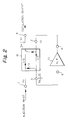
- Fig.1A is converted to Fig.2, in which V in is input signal voltage, and V f is output of an amplifier.
- An output voltage V out is expressed as follows.
- the four-port network 10 operates as mentioned above at any frequencies, when an input signal with high stability and low phase noise is applied to the input port 1, half of said input signal is applied to amplifier 11 through port 3, and harmonics are generated in the amplifier 11 due to non-linearity of the amplifier under oscillation.
- frequency of said harmonics are close to the oscillation frequency, beat is generated between said harmonics and the oscillation frequency. And then, the circuit conditions shift so that said beat frequency converges to zero, so that the oscillation frequency is locked to the injection frequency.
- non-reciprocal four-port network 10 may be implemented by the combination of four non-reciprocal amplifiers each located at the portion indicated by an arrow in the figure. In that case, the gain of each amplifier is not necessarily higher than 1, but an amplifier with gain less than 1 would be enough.
- Fig.1B shows a modification of Fig.1A.
- the feature of Fig.1B is that no non-reciprocal signal path from the first input port 1 to the second output port 2 is provided. That signal transfer path from port 1 to port 2 is not necessary for the operation of an injection locked oscillator.
- the circuit may be symmetrical if a signal transfer path from port 1 to 3 exists, and therefore, operational frequency range would be wide.
- the numerals 21, 22, 31, and 32 are a common-gate field effect transistor (FET).
- Numerals 20 and 30 are a in-phase divider having a pair of said FET's.
- S indicates a source
- D is a drain
- G is a gate.
- Numeral 11 is an amplifier
- lla is a variable phase shifter circuit having a line L, and a pair of variable capacitors C 1 and C 2 .
- the phase shift circuit lla adjusts free running frequency of the oscillator by controlling the capacitance of the capacitors C 1 and C 2 .
- An in-phase divider 20 and 30 operate as follows.
- An input signal applied to port 23 (or 33) is divided to the output ports 24 and 25 (or 34 and 35) with the same phase, because of the symmetry of the circuit.
- the signal transfer ratios S 21 and S 31 from port 23 (or 33) to ports 24 and 25 (or 34 and 35) is as follow.
- Said value S 21 is 1/2 when port 23(or 33) is in impedance matching condition.
- the signal transfer from ports 24 and 25 (or 34 and 35) to port 23 (or 33) is prevented because of the non-reciprocity of an FET, and therefore, the signal transfer between the output ports 24 and 25 (or 34 and 35) is prevented.
- the non-reciprocal four-port network 10 having the power divider circuits 20 and 30 satisfies S 11 , S 12 , and S 13 are less than -20dB in the frequency range from DC to 18 GHz, as shown in the article "Very Small Ultra-Wide-Band MMIC Magic T and Applicatoins to combiners and Deviders" (T.Tokumitsu et al., IEEE Trans., vol.MTT-37, No.12, 1989). Since the cut-off frequency of an FET used is 20-23 GHz, said non-reciprocal four-port network, and/or the divider circuits, operates up to the cut-off frequency of a transistor element itself.
- Said non-reciprocal four-port network is also implemented by using differential amplifiers, JP patent laid open 158008/1991, and JP patent laid open 58902/1990), with the similar operation as mentioned above.
- the distribution ratio of a divider is assumed to be 1:1 in the above explanation, but it should be appreciated that another ratio is of course possible so long as the gain in the loop 2-3-5-6-2 is higher than 1.
- the present injection-locked oscillator is implemented by using only a transistor circuit, but no distribution constant circuit such as a quarter wavelength line is used. Therefore, the present oscillator is implemented on a single chip and packed in a small package along with semiconductor IC, or a microwave IC with small size, that is a frequency converter. As a commercial miniature package is enough for implementing the oscillator module, the producing cost may be low.
- the present oscillator may be locked to frequency within the operation frequency band of an amplifier and/or 1/n of that frequency, to provide high stability and low phase noise signal. Therefore, the selection for an injection signal generator is arbitrary.
- an injection signal generator IC is implemented for instance by a synthesizer for mobile communication
- the present oscillator module is implemented by only two IC chips. Therefore, the present oscillator is simple and economical as compared with a prior PLL circuit which has many package IC's including a voltage controlled oscillator, a power divider circuit, a frequency divider, a phase comparator, and a low-pass filter.
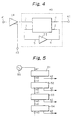
- Fig.4 shows another embodiment of the present injection-locked oscillator.
- numeral 40 is an injection-locked oscillator mentioned in the previous embodiment
- 44 is a multi-outputs amplifier having one input port and two output ports
- 41 is an injection signal input port
- 42 is an oscillation output port
- 43 is a second output port of an amplifier 44.
- Fig.4 has the feature of the presence of amplifier 44, so that level of an input signal at an port 41 can be low. Further, since amplifier 44 provides an output signal at a port 43 with amplified high level, said output signal at 43 is used as an injection input signal for a succeeding injection-locked oscillator which is locked with no deterioration of injection-locking bandwidth. Therefore, a plurality of injection-locked oscillators may be locked with a common injection input signal. Conventionally, when a plurality of injection-locked oscillators are locked with a single injection input signal, a parallel multi-divider having a Willkinson divider is used for dividing an input signal, and therefore, the whole apparatuses must be located on a secondary dimensional plane.
- a plurality of injection-locked oscillators may be arranged either linearly, or secondary dimensional plane or third dimensional space. Further, since the path between an input port and output ports, and the path between output ports of a multi-output amplifier are electrically isolated, each injection oscillator operates independently from another injection-locked oscillator. Further, since the operation frequency of a multi-output amplifier 44 is only 1/n of that of an injection-locked oscillator 40, operation frequency of said amplifier 44 and its related circuit may be low.
- Fig.5 shows an embodiment in which a plurality of injection-locked oscillators are arranged linearly.
- Numeral 50 is a common injection source, which applies an injection signal with high stability and low phase noise to a first injection-locked oscillator 51 which has the structure of Fig.4.
- the first oscillator 51 provides not only a locked output at the output port 42, but also the second output for injection input signal for a succeeding oscillator 52 at port 43.
- the second injection-locked oscillator 52 is locked with an injection input which is provided at port 43 of the first oscillator 51.
- the succeeding oscillators 53, 54 et a1 are locked to a common injection source 50.
- the structure of Fig.5 may be used in any point between injection-locked oscillators, and therefore, no severe condition for arrangement such as a prior parallel multi-divider circuit is necessary.
- phase shifter or a delay line between adjacent injection-locked oscillators (between ports 43 and 41) provide desirable phase relations between oscillation output signals.
- phase shifters or delay lines having suitable phase shift or delay time provide the various phases in the output signals. That allows to feed an array antenna.
- the present invention has a non-reciprocal four-port network having a pair of input ports and a pair of output ports so that the signal transfers from a first input port to a first output port, from a second input port to a first output port and from a second input port to a second output port are non-reciprocal, and the circuits between a first input port and a second input port and between a first output port and a second output port are electrically isolated, and an amplifier with operation frequency band which is a part of operation frequency band of said four-port network. Said amplifier is coupled between a first output port of said four-port network and a second input port of said four-port network.
- a first input port of the four-port network is an input port of an injection-locked oscillator, and a second output port of the four-port network is an output port of said oscillator.
- a multi-output amplifier may be inserted between an input port of the oscillator and a first input port of the four-port network.
- the present oscillator is implemented only by using transistors, or at least a main component is a transistor. Therefore, no quarter wavelength circuit which is bulk and/or no circuit having ferrite is necessary, so that the present oscillator is packed into a small IC chip. Because of the non-reciprocity of a four-port network, an oscillation loop (2-3-5-6-2), an injection signal input, and an oscillation output are electrically isolated with one another. Therefore, the present oscillator is not affected by an external circuit, and/or an external load. Further, the present oscillator has very wide operation frequency band because of the wide operation frequency band of a transistor so that the oscillator may be locked to an injection signal of wide frequency band, and subharmonic coefficient n may be designed arbitrary.
- a local oscillator in a transmitter and/or a receiver may be obtained by combining the present oscillator with a commercially obtained synthesizer.
- an injection signal is amplified so that it is injected to a succeeding oscillator with no attenuation of an injection signal
- a plurality of oscillators may be locked to a common injection signal without restricting operation band of synchronization.
- the present invention is applicable to feed an array antenna by inserting a phase shifter between adjacent oscillators. Since the oscillators may be located either linearly, or in secondary dimensional plane, or in third dimensional space, the freedom of beam formation of an array antenna is improved.
- the loop gain may be controlled either higher than 1 or lower than 1 by adjusting the gain of said amplifier, so that the oscillation is switched ON and OFF. That feature is applicable to frequency switching, and/or frequency hopping communication.
Landscapes
- Stabilization Of Oscillater, Synchronisation, Frequency Synthesizers (AREA)
- Inductance-Capacitance Distribution Constants And Capacitance-Resistance Oscillators (AREA)
- Amplifiers (AREA)
- Microwave Amplifiers (AREA)
Claims (7)
- Injektionssynchronisierter Oszillator mit:dadurch gekennzeichnet, daßeinem nichtreziproken Vierpol-Netzwerk (10), das einen ersten Eingangsanschluß (1), einen zweiten Eingangsanschluß (2), einen ersten Ausgangsanschluß (3) und einen zweiten Ausgangsanschluß (4) aufweist,einem Verstärker (11) mit einem Eingang (5), der mit dem ersten Ausgangsanschluß verbunden ist und einen Ausgang (6) aufweist, der mit dem zweiten Eingangsanschluß verbunden ist, und mit einem Betriebsfrequenzbereich in wenigstens einem Teil des Betriebsfrequenzbereichs des Vierpol-Netzwerks,einem mit dem ersten Eingangsanschluß des Vierpol-Netzwerks verbundenen Injektionssignal-Eingangsanschluß undeinem mit dem zweiten Ausgangsanschluß des Vierpol-Netzwerks verbundenen Schwingungs-Ausgangsanschluß,
das nichtreziproke Vierpol-Netzwerk so ausgebildet ist, daß ein Signalübertragungskanal vom ersten Eingangsanschluß zum ersten Ausgangsanschluß nichtreziprok ist, ein Signalübertragungskanal vom zweiten Eingangsanschluß zum zweiten Ausgangsanschluß nichtreziprok ist und ein Signalübertragungskanal vom zweiten Eingangsanschluß zum ersten Ausgangsanschluß nichtreziprok ist, und daß der Kanal zwischen dem ersten Eingangsanschluß und dem zweiten Eingangsanschluß sowie der Kanal zwischen dem ersten Ausgangsanschluß und dem zweiten Ausgangsanschluß elektrisch isoliert sind, d.h. keine Signalübertragung auf den beiden zuletzt erwähnten Kanälen erfolgt. - Injektionssynchronisierter Oszillator nach Anspruch 1, bei dem ein Mehrausgang-Verstärker (44) mit einem einzigen Eingang (41) und mehreren Ausgängen zwischen dem Injektionssignal-Eingangsanschluß und dem ersten Anschluß des Vierpol-Netzwerks angeschlossen ist, so daß jeder Ausgang des Mehrausgang-Verstärkers mit dem ersten Anschluß des Vierpol-Netzwerks eines zugehörigen injektionssynchronisierten Oszillators verbunden ist.
- Injektionssynchronisierter Oszillator nach Anspruch 1, bei dem ein nichtreziproker Signalübertragungskanal vom ersten Eingangsanschluß zum zweiten Ausgangsanschluß des Vierpol-Netzwerks vorgesehen ist.
- Injektionssynchronisierter Oszillator nach Anspruch 1, bei dem jeder Signalübertragungskanal in dem Vierpol-Netzwerk einen nichtreziproken Verstärker aufweist.
- Injektionssynchronisierter Oszillator nach Anspruch 4, bei dem der nichtreziproke Verstärker einen Feldeffekt-Transistor (21, 22, 31, 32) mit einem geerdeten Gate, einer Source und einer Drain in jedem Signalübertragungskanal aufweist.
- Injektionssynchronisierter Oszillator nach Anspruch 4, bei dem eine veränderbare Phasenschieberschaltung (11a) in Reihe mit dem Verstärker (11) angeordnet ist, deren Betriebsfrequenzbereich in wenigstens einem Teil des Betriebsfrequenzbereichs des Vierpol-Netzwerks liegt.
- Injektionssynchronisierte Oszillatoranordnung mit mehreren injektionssynchronisierten Oszillatoren (51-54), die jeweils aufweisen:dadurch gekennzeichnet, daßeinen Mehrausgang-Verstärker (44) mit einem Eingangsanschluß (41) und zwei Ausgangsanschlüssen,ein nichtreziprokes Vierpol-Netzwerk mit einem ersten Eingangsanschluß (1) und einem zweiten Eingangsanschluß (2) sowie einem ersten Ausgangsanschluß (3) und einem zweiten Ausgangsanschluß (4),einen Verstärker (11) mit einem Eingang (5), der mit dem ersten Ausgangsanschluß des nichtreziproken Vierpol-Netzwerks verbunden ist, und einem Ausgang (6), der mit dem zweiten Eingangsanschluß des nichtreziproken Vierpol-Netzwerks verbunden ist, wobei der Betriebsfrequenzbereich des Verstärkers in wenigstens einem Teil des Betriebsfrequenzbereichs des Vierpol-Netzwerks liegt,einen mit dem ersten Eingangsanschluß des nichtreziproken Vierpol-Netzwerks verbundenen Injektionssignal-Eingangsanschluß (41) undeinen Schwingungs-Ausgangsanschluß (42), der mit dem zweiten Ausgangsanschluß des nichtreziproken Vierpol-Netzwerks verbunden ist, wobeiein erster Ausgangsanschluß jedes Mehrausgang-Verstärkers, der mit einem ersten Eingangsanschluß (1) eines nichtreziproken Vierpol-Netzwerks eines injektionssynchronisierten Oszillators in derselben Stufe wie der des Mehrausgang-Verstärkers verbunden ist, und ein zweiter Ausgangsanschluß (43) jedes Mehrausgang-Verstärkers mit einem Eingangsanschluß des Mehrausgang-Verstärkers in einer folgenden Stufe verbunden ist,
das nichtreziproke Vierpol-Netzwerk so ausgebildet ist, daß ein Signalübertragungskanal von einem ersten Eingangsanschluß zu einem ersten Ausgangsanschluß nichtreziprok ist, ein Signalübertragungskanal von einem zweiten Eingangsanschluß zu einem zweiten Ausgangsanschluß nichtreziprok ist und ein Signalübertragungskanal von einem zweiten Eingangsanschluß zu einem ersten Ausgangsanschluß nichtreziprok ist und daß der Kanal zwischen dem ersten Eingangsanschluß und dem zweiten Eingangsanschluß sowie der Kanal zwischen dem ersten Ausgangsanschluß und dem zweiten Ausgangsanschluß elektrisch isoliert sind, d.h. auf den beiden zuletzt erwähnten Kanälen keine Signalübertragung erfolgt.
Applications Claiming Priority (3)
| Application Number | Priority Date | Filing Date | Title |
|---|---|---|---|
| JP24908/94 | 1994-01-28 | ||
| JP2490894 | 1994-01-28 | ||
| JP6024908A JPH07221546A (ja) | 1994-01-28 | 1994-01-28 | 注入同期発振器 |
Publications (2)
| Publication Number | Publication Date |
|---|---|
| EP0665652A1 EP0665652A1 (de) | 1995-08-02 |
| EP0665652B1 true EP0665652B1 (de) | 2001-03-28 |
Family
ID=12151282
Family Applications (1)
| Application Number | Title | Priority Date | Filing Date |
|---|---|---|---|
| EP95400171A Expired - Lifetime EP0665652B1 (de) | 1994-01-28 | 1995-01-26 | Injektionssynchronisierter Oszillator |
Country Status (4)
| Country | Link |
|---|---|
| US (1) | US5546056A (de) |
| EP (1) | EP0665652B1 (de) |
| JP (1) | JPH07221546A (de) |
| DE (1) | DE69520459T2 (de) |
Cited By (1)
| Publication number | Priority date | Publication date | Assignee | Title |
|---|---|---|---|---|
| WO2019125326A3 (en) * | 2017-07-27 | 2019-09-19 | Feyzi̇ye Mektepleri̇ Vakfi Işik Üni̇versi̇tesi̇ | Universal 4-port mutator |
Families Citing this family (12)
| Publication number | Priority date | Publication date | Assignee | Title |
|---|---|---|---|---|
| US6212397B1 (en) * | 1996-12-23 | 2001-04-03 | Texas Instruments Incorporated | Method and system for controlling remote multipoint stations |
| US20030209499A1 (en) * | 2000-09-29 | 2003-11-13 | Haase Richard A. | Clarification of water and wastewater |
| US6208214B1 (en) * | 2000-02-04 | 2001-03-27 | Tlc Precision Wafer Technology, Inc. | Multifunction high frequency integrated circuit structure |
| JP4193382B2 (ja) * | 2001-07-19 | 2008-12-10 | 株式会社日立製作所 | 磁場計測装置 |
| JP4055202B2 (ja) | 2002-05-17 | 2008-03-05 | 日本電気株式会社 | 基準振動発生装置、その相互同期化系およびその相互同期化方法 |
| US7068115B2 (en) | 2002-09-13 | 2006-06-27 | Tlc Precision Wafer Technology, Inc. | Monolithic microwave integrated circuit voltage controlled coupled feedback oscillator |
| US6977557B1 (en) | 2004-03-25 | 2005-12-20 | Marvin Elmer Frerking | Injection mode steering oscillator |
| JP4299283B2 (ja) | 2005-09-16 | 2009-07-22 | 富士通株式会社 | クロック信号の生成及び分配装置 |
| US9374100B2 (en) * | 2009-07-01 | 2016-06-21 | Qualcomm Incorporated | Low power LO distribution using a frequency-multiplying subharmonically injection-locked oscillator |
| US8811926B2 (en) * | 2010-03-23 | 2014-08-19 | University Of Washington Through Its Center For Commercialization | Frequency multiplying transceiver |
| US9154145B2 (en) | 2011-05-02 | 2015-10-06 | Rambus Inc. | Integrated circuit having a multiplying injection-locked oscillator |
| JP5811863B2 (ja) * | 2012-01-26 | 2015-11-11 | 富士通株式会社 | クロック分配器、及び、電子装置 |
Family Cites Families (2)
| Publication number | Priority date | Publication date | Assignee | Title |
|---|---|---|---|---|
| JPS58209232A (ja) * | 1982-05-31 | 1983-12-06 | Nec Corp | 発振回路 |
| JPS59161925A (ja) * | 1983-03-07 | 1984-09-12 | Mitsubishi Electric Corp | 注入同期発振器 |
-
1994
- 1994-01-28 JP JP6024908A patent/JPH07221546A/ja not_active Withdrawn
-
1995
- 1995-01-26 DE DE69520459T patent/DE69520459T2/de not_active Expired - Fee Related
- 1995-01-26 EP EP95400171A patent/EP0665652B1/de not_active Expired - Lifetime
- 1995-01-27 US US08/378,952 patent/US5546056A/en not_active Expired - Fee Related
Cited By (1)
| Publication number | Priority date | Publication date | Assignee | Title |
|---|---|---|---|---|
| WO2019125326A3 (en) * | 2017-07-27 | 2019-09-19 | Feyzi̇ye Mektepleri̇ Vakfi Işik Üni̇versi̇tesi̇ | Universal 4-port mutator |
Also Published As
| Publication number | Publication date |
|---|---|
| JPH07221546A (ja) | 1995-08-18 |
| DE69520459D1 (de) | 2001-05-03 |
| US5546056A (en) | 1996-08-13 |
| EP0665652A1 (de) | 1995-08-02 |
| DE69520459T2 (de) | 2001-08-23 |
Similar Documents
| Publication | Publication Date | Title |
|---|---|---|
| Yabuki et al. | Stripline dual-mode ring resonators and their application to microwave devices | |
| US5546056A (en) | Injection-locked oscillator having non-reciprocal four port network | |
| JP3851900B2 (ja) | 平面フィルタ、半導体装置、および無線装置 | |
| US4692714A (en) | Single resonator push-push oscillator | |
| US7164902B2 (en) | Filter-integrated even-harmonic mixer and hi-frequency radio communication device using the same | |
| US6133795A (en) | Oscillator circuit | |
| US4992761A (en) | Passive 180 degree broadband MMIC hybrid | |
| CN107910629A (zh) | 一种低相位噪声基片集成波导振荡器 | |
| EP0760954B1 (de) | Phasenrauschendetektor | |
| KR20010098933A (ko) | 발진기 및 통신기 장치 | |
| EP2086107B1 (de) | Oszillator, sende-/empfangseinrichtung und frequenzsynthesizer | |
| EP0906657B1 (de) | Frequenzumsetzer für millimeterwellen | |
| Kawahata et al. | A K-band push-push oscillator with high suppression of undesired harmonic signals | |
| US3818365A (en) | Microwave amplifier circuit utilizing negative resistance diode | |
| Tokumitsu et al. | A novel injection-locked oscillator MMIC with combined ultrawide-band active combiner/divider and amplifiers | |
| Lee et al. | High power microwave signal generation based on recursive balanced power amplifier | |
| US6614329B1 (en) | Radio frequency/microwave/millimeterwave filter | |
| US6771137B2 (en) | High-frequency oscillator | |
| KR20030009352A (ko) | 다기능의 고주파 집적 회로 구조물 | |
| Weber et al. | A PLL-stabilized W-band MHEMT push-push VCO with integrated frequency divider circuit | |
| US6297707B1 (en) | Microwave oscillator with dielectric resonator | |
| US5519359A (en) | Microwave oscillator with loop frequency conversion to and signal amplification at an intermediate frequency | |
| Schunemann et al. | Components for microwave integrated circuits with evanescent-mode resonators | |
| US4270099A (en) | Circuit arrangement for generating and stably amplifying broadband rf signals | |
| Grubinger et al. | Continuous tunable phase shifter based on injection locked local oscillators at 30 GHz |
Legal Events
| Date | Code | Title | Description |
|---|---|---|---|
| PUAI | Public reference made under article 153(3) epc to a published international application that has entered the european phase |
Free format text: ORIGINAL CODE: 0009012 |
|
| 17P | Request for examination filed |
Effective date: 19950130 |
|
| AK | Designated contracting states |
Kind code of ref document: A1 Designated state(s): DE FR GB |
|
| RAP1 | Party data changed (applicant data changed or rights of an application transferred) |
Owner name: NIPPON TELEGRAPH AND TELEPHONE CORPORATION |
|
| 17Q | First examination report despatched |
Effective date: 19961227 |
|
| GRAG | Despatch of communication of intention to grant |
Free format text: ORIGINAL CODE: EPIDOS AGRA |
|
| GRAG | Despatch of communication of intention to grant |
Free format text: ORIGINAL CODE: EPIDOS AGRA |
|
| GRAH | Despatch of communication of intention to grant a patent |
Free format text: ORIGINAL CODE: EPIDOS IGRA |
|
| GRAH | Despatch of communication of intention to grant a patent |
Free format text: ORIGINAL CODE: EPIDOS IGRA |
|
| GRAA | (expected) grant |
Free format text: ORIGINAL CODE: 0009210 |
|
| AK | Designated contracting states |
Kind code of ref document: B1 Designated state(s): DE FR GB |
|
| REF | Corresponds to: |
Ref document number: 69520459 Country of ref document: DE Date of ref document: 20010503 |
|
| ET | Fr: translation filed | ||
| REG | Reference to a national code |
Ref country code: GB Ref legal event code: IF02 |
|
| PLBE | No opposition filed within time limit |
Free format text: ORIGINAL CODE: 0009261 |
|
| STAA | Information on the status of an ep patent application or granted ep patent |
Free format text: STATUS: NO OPPOSITION FILED WITHIN TIME LIMIT |
|
| 26N | No opposition filed | ||
| PGFP | Annual fee paid to national office [announced via postgrant information from national office to epo] |
Ref country code: DE Payment date: 20050115 Year of fee payment: 11 |
|
| PGFP | Annual fee paid to national office [announced via postgrant information from national office to epo] |
Ref country code: GB Payment date: 20050126 Year of fee payment: 11 |
|
| PGFP | Annual fee paid to national office [announced via postgrant information from national office to epo] |
Ref country code: FR Payment date: 20050128 Year of fee payment: 11 |
|
| PG25 | Lapsed in a contracting state [announced via postgrant information from national office to epo] |
Ref country code: GB Free format text: LAPSE BECAUSE OF NON-PAYMENT OF DUE FEES Effective date: 20060126 |
|
| PG25 | Lapsed in a contracting state [announced via postgrant information from national office to epo] |
Ref country code: FR Free format text: LAPSE BECAUSE OF NON-PAYMENT OF DUE FEES Effective date: 20060131 |
|
| PG25 | Lapsed in a contracting state [announced via postgrant information from national office to epo] |
Ref country code: DE Free format text: LAPSE BECAUSE OF NON-PAYMENT OF DUE FEES Effective date: 20060801 |
|
| GBPC | Gb: european patent ceased through non-payment of renewal fee |
Effective date: 20060126 |
|
| REG | Reference to a national code |
Ref country code: FR Ref legal event code: ST Effective date: 20060929 |