EP0664616A2 - Durch eine kalibrierte Oszillatorsteuergrösse initialisierter Phasenregelkreis - Google Patents
Durch eine kalibrierte Oszillatorsteuergrösse initialisierter Phasenregelkreis Download PDFInfo
- Publication number
- EP0664616A2 EP0664616A2 EP95300148A EP95300148A EP0664616A2 EP 0664616 A2 EP0664616 A2 EP 0664616A2 EP 95300148 A EP95300148 A EP 95300148A EP 95300148 A EP95300148 A EP 95300148A EP 0664616 A2 EP0664616 A2 EP 0664616A2
- Authority
- EP
- European Patent Office
- Prior art keywords
- oscillator
- phase
- control signal
- control
- lock loop
- Prior art date
- Legal status (The legal status is an assumption and is not a legal conclusion. Google has not performed a legal analysis and makes no representation as to the accuracy of the status listed.)
- Withdrawn
Links
Images

Classifications
-
- H—ELECTRICITY
- H03—ELECTRONIC CIRCUITRY
- H03L—AUTOMATIC CONTROL, STARTING, SYNCHRONISATION OR STABILISATION OF GENERATORS OF ELECTRONIC OSCILLATIONS OR PULSES
- H03L7/00—Automatic control of frequency or phase; Synchronisation
- H03L7/06—Automatic control of frequency or phase; Synchronisation using a reference signal applied to a frequency- or phase-locked loop
- H03L7/08—Details of the phase-locked loop
- H03L7/14—Details of the phase-locked loop for assuring constant frequency when supply or correction voltages fail
- H03L7/146—Details of the phase-locked loop for assuring constant frequency when supply or correction voltages fail by using digital means for generating the oscillator control signal
-
- H—ELECTRICITY
- H03—ELECTRONIC CIRCUITRY
- H03L—AUTOMATIC CONTROL, STARTING, SYNCHRONISATION OR STABILISATION OF GENERATORS OF ELECTRONIC OSCILLATIONS OR PULSES
- H03L3/00—Starting of generators
-
- H—ELECTRICITY
- H03—ELECTRONIC CIRCUITRY
- H03L—AUTOMATIC CONTROL, STARTING, SYNCHRONISATION OR STABILISATION OF GENERATORS OF ELECTRONIC OSCILLATIONS OR PULSES
- H03L7/00—Automatic control of frequency or phase; Synchronisation
- H03L7/06—Automatic control of frequency or phase; Synchronisation using a reference signal applied to a frequency- or phase-locked loop
- H03L7/08—Details of the phase-locked loop
- H03L7/10—Details of the phase-locked loop for assuring initial synchronisation or for broadening the capture range
-
- H—ELECTRICITY
- H04—ELECTRIC COMMUNICATION TECHNIQUE
- H04J—MULTIPLEX COMMUNICATION
- H04J3/00—Time-division multiplex systems
- H04J3/02—Details
- H04J3/06—Synchronising arrangements
- H04J3/0635—Clock or time synchronisation in a network
- H04J3/0685—Clock or time synchronisation in a node; Intranode synchronisation
- H04J3/0688—Change of the master or reference, e.g. take-over or failure of the master
Definitions
- This invention relates to phase-lock loop circuits.
- Phase-lock loops (also sometimes referred to as phase-locked loops) are well-known circuits.
- a phase-lock loop Conventionally used as a clock-frequency generator in telecommunications systems, a phase-lock loop locally generates an output signal stream that is referenced to or locked to (i.e., that tracks) a remotely-supplied reference input signal stream, in both frequency and phase. Both analog and digital implementations of phase-lock loops are well known.
- the basic configuration of a phase-lock loop includes an oscillator that generates the local output signal.
- the oscillator output is fed as an input to a phase comparator, along with the remote reference signal.
- Output of the phase comparator which is representative of the frequency and phase difference of its two inputs, is fed to a controller that converts this difference signal into a control signal for the oscillator. Under influence of the control signal, the output of the oscillator is adjusted to track the remotely-supplied reference input signal.
- the phase-lock loop upon power-up (start-up) of the phase-lock loop and before it has had time to lock onto the reference input signal, or upon loss of the reference input signal following the phase-lock loop having locked thereunto, the phase-lock loop has been operated in a "free running" mode. That is, the output signal generated by the phase-lock loop has been the output of the oscillator operating free of any adjustment to its operation being made by the controller.
- the output of the phase-lock loop to be useful while "free running", it has been necessary to use a very precise and stable oscillator that could be depended upon to independently operate very precisely at the reference signal's frequency, and to not drift in frequency and phase over very long periods of time (e.g., years).
- oscillators are very expensive.
- holdover To avoid the use of a very expensive oscillator yet still ensure that the phase-lock loop output remains stable during temporary loss of the reference input signal, a capability known as “holdover” has been developed and is well-known in the art. This capability involves temporarily latching the control signal generated by the controller immediately prior to the loss of the reference input signal, and continuing to use the latched control signal to control the output of the oscillator during the time period when the reference input signal is not available.
- the "holdover" capability has done nothing to solve the problem of "free running" operation of a phase-lock loop with an inexpensive --imprecise and unstable-- oscillator during power-up, and particularly during power-up in the absence of the reference input signal, because a "holdover" control signal is not available to the phase-lock loop at power-up, and thereafter until the reference input signal becomes available. Consequently, the problems that result from operating a phase-lock loop with an imprecise and unstable oscillator have not been fully solved by the prior art.
- the phase-lock loop is initialized at power-up by an oscillator-control signal that has previously been stored in a non-volatile manner.
- a phase-lock loop that comprises an oscillator for generating an output signal under influence of a control signal and an oscillator control coupled to the oscillator for generating the control signal under influence of a received reference signal
- an arrangement is provided which responds to receipt by the oscillator control of a predetermined said reference signal (e.g., a calibrated reference signal) by storing the (calibrated) control signal, that is generated by the oscillator control under the influence of the predetermined reference signal, in a non-volatile manner (e.g., in a non-volatile memory).
- the arrangement supplies the stored control signal to the oscillator to influence generation of the output signal at power-up instead of the control signal -- if any -- that is generated at power-up by the oscillator control.
- the operation of the phase-lock loop at power-up is no longer "free-running", but is controlled by an oscillator control signal as at other times during the operation of the phase-lock loop. Since the operation at power-up is controlled, the problems associated with operating a phase-lock loop with an inexpensive, imprecise and unstable, oscillator at power-up in "free running" mode are alleviated.
- the control signal continues to exist and is available for controlling the oscillator at power-up.
- the stored control signal is not generated as a function of just any reference signal, but is generated only on the basis of a predetermined reference signal such as a calibrated reference signal, it is possible to ensure that the stored control signal is one that will yield the generation by the oscillator of a high-quality output signal typical of greatly more expensive oscillators.
- the above-characterized arrangement is implemented as a digital processor operating under stored-program control.
- Such an implementation is simple to construct, and is readily modified for use in different environments and for different applications. And since many systems that make use of phase-lock loops already include digital processors with spare processing capacity that may be used for this purpose, this implementation adds little or no hardware and very little cost to the overall system.
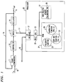
- FIG. 1 shows a conventional phase-lock loop modified according to the present invention.
- the conventional phase-lock loop includes a phase comparator 11 that receives a locally-generated signal stream over a link 16, and a remotely-supplied reference signal stream f in over a link 10.
- Phase comparator determines the phase difference between the two received signals and supplies a signal indicative of that difference to a controller 12. This phase difference over a long period of time indicates a frequency difference between these two signals.
- Controller 12 converts the indicated difference into a control signal which it supplies to an oscillator 14 through a switch 13.
- Controller 12 illustratively comprises a low-pass filter.
- Oscillator 14 generates an output signal stream f out on a link 15, and it responds to the received control signal by adjusting the frequency and/or phase of output signal f out accordingly.
- Oscillator 14 illustratively comprises a voltage-controlled crystal oscillator or a digital frequency synthesizer. A sample of output signal f out is fed back to phase comparator 11 via link 16.
- the phase-lock loop of FIG. 1 may be either an analog or a digital phase-lock loop.
- Switch 13 or a functional equivalent is conventionally used in conjunction with provisioning of the "holdover” function to provide a “holdover” control signal value in place of the output of controller 12 to oscillator 14 when f in is temporarily lost.
- switch 13 is used to couple a digital processor 20 to the phase-lock loop.
- Processor 20 is illustratively any suitable conventional and commercially-available microprocessor. It comprises a central processing unit (CPU) 22 that includes at least one register 23 for temporarily storing a data item, a read-only memory (ROM) 24 that holds programs which CPU 22 executes, and a non-volatile memory 27 that is both readable and writable and that stores data for use by CPU 22 during program execution.
- the non-volatile nature of memory 27 ensures that data stored therein do not disappear therefrom when the phase-lock loop and processor 20 of FIG. 1 are unpowered, but rather ensures that the data are immediately available to processor 20 upon power-up.
- CPU 22 is connected to switch 13 through an input and output (I/O) interface 21 and a link 17. I/O interface 21 and a link 18 serve to also connect processor 20 to "the outside world", e.g., other circuitry of any system that the phase-lock loop of FIG. 1 is a part of.
- Processor 20 performs the conventional "holdover" function by executing a holdover function program 25 out of ROM 24. While the phase-lock loop of FIG. 1 is powered up and operating, processor 20 is appraised via link 18 of the presence or absence of reference signal f in on link 10. While f in is present, processor 20 monitors the value of the oscillator control signal being generated by controller 12 via switch 13, and repeatedly stores the present value of this control signal in register 23. When f in becomes absent, processor 20 causes switch 13 to disconnect the output of controller 12 from the control input of oscillator 14, and instead processor 20 supplies the control signal value stored in register 23 to the control input of oscillator 14 via switch 13. When f in is restored, processor 20 ceases to supply the control-signal value from register 23 to oscillator 14, causes switch 13 to reconnect the output of controller 12 to oscillator 14, and resumes repeatedly storing in register 23 the present value of the control signal being generated by controller 12.
- processor 20 performs a calibration function 26 and a related loop initialization function 29.
- calibration function 26 will initially be performed before a system of which the phase-lock loop and processor 20 of FIG. 1 are a part is placed into service, e.g., as part of the final stage of manufacturing the system.
- a source of accurate reference signal f in i.e., a calibrated source
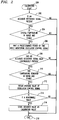
- processor 20 executes calibration function 26, which is flowcharted in FIG. 2.
- processor 20 Upon receipt of the calibration command, at step 200, processor 20 checks whether an accurate reference signal is present, at step 202. How this determination is made will vary from system to system. For example, in a telephony transmissions system operating under the Synchronous Digital Hierarchy (SDH) standard, processor 20 checks for receipt by the system of a synchronization status message byte (SSMB) informing the system that the incoming f in is created by a primary clock source. An alternative check may involve receipt by processor 20 via link 18 of a command manually entered by a craftsperson, which either informs processor 20 that a calibrated source of f in is connected to link 10 or which causes processor 20 to skip the check of step 202.
- SDH Synchronous Digital Hierarchy
- processor 20 terminates calibration function 26, at step 218. If it is not determined at step 202 that accurate reference signal f in is present, processor 20 terminates calibration function 26, at step 218. If it determined at step 202 that accurate reference signal f in is present or if the step is omitted, processor 20 checks whether the system's ambient temperature is in a predefined range and is stable, at step 204. Illustratively, processor 20 obtains this information by querying other units of the system of which the phase-lock loop and processor 20 are a part. The reason for the check is to ensure that the performance of oscillator 14 is not being unduly affected by temperature. If oscillator 14 is immune to system temperature (for example, if oscillator 14 is an ovenized or a temperature-compensated oscillator), then the check of step 204 may be omitted.
- processor 20 terminates calibration function 26, at step 218. If it is determined at step 204 that system temperature is in range and stable or if the step is omitted, processor 20 commences to monitor the oscillator control signal being generated by controller 12 and does so for a predetermined period of time referred to as the calibration interval, at step 206, to ensure that the phase-lock loop has had sufficient opportunity to lock onto the reference signal f in . Processor 20 then repeats the checks of steps 202 and 204, at steps 208 and 210, respectively, to ensure that the requisite conditions for proper calibration have continued to exist throughout the calibration interval. These checks may likewise be omitted based on the same criteria as were discussed in conjunction with steps 202 and 204.
- processor 20 obtains the average value of the oscillator control signals generated by controller 12 and monitored during the calibration interval, at step 212. Processor 20 then checks whether this average value is reasonable, at step 214. Illustratively, processor 20 performs this check by comparing the average control value against a presently-stored calibration value 28 retrieved from non-volatile memory 27 to determine whether the average control value is within a predetermined range of the presently-stored calibration value 28; if there is no presently-stored calibration value 28, processor 20 merely accepts the average control value as being reasonable. If processor 20 finds at step 214 that the average control value is not reasonable, it terminates calibration function 26, at step 218.
- processor 20 finds at step 214 that the average control value is reasonable, it stores the average control value as calibration value 28 in non-volatile memory 27, along with a time-stamp that indicates the date and time of creation of the calibration value, at step 216, and then terminates calibration function 26, at step 218.
- Processor 20 may now be unpowered, along with the rest of the system of which it is a part. Due to the non-volatile nature of memory 27, calibration value 28 is not lost, but remains available to processor 20 upon subsequent power-up of processor 20. Upon that subsequent power-up, e.g., upon the system of which the phase-lock loop and processor 20 are a part being placed in, or being returned to, service, processor 20 executes loop initialization function 29, which is flowcharted in FIG. 3.
- processor 20 In response to invocation of loop initialization function 29, at step 300, processor 20 causes switch 13 to disconnect the control output of controller 12 from the control input of oscillator 14, at step 302.
- Processor 20 retrieves the previously-stored calibration value 28 from non-volatile memory 27, at step 304, and supplies this value 28 to the control input of oscillator 14 on an ongoing basis, at step 306, in place of any control signal that may be generated by controller 12 at this time.
- This causes oscillator 14 to generate an output signal stream f out that is the same in both frequency and phase as what oscillator 14 generated when the phase-lock loop of FIG. 1 was last calibrated with an accurate reference signal f in .
- processor 20 When processor 20 receives via link 18 a directive to allow controller 12 to take over control of oscillator 14 and lock the output f out of the phase-lock loop to the input f in , at step 310, it first checks whether f in is presently available, at step 312. Illustratively, processor 20 performs this check by interrogating other circuitry of the system of which the phase-lock loop and processor 20 are a part, via link 18. If processor 20 determines at step 312 that f in is not available, it continues the present mode of operation while it waits at step 312 for f in to become available.
- processor 20 determines at step 312 that f in is available, processor 20 causes switch 13 to reconnect the control output of controller 12 to the control input of oscillator 14, at step 314, thereby putting oscillator 14 under control of controller 12, and ceases to supply calibration value 28 to oscillator 14, at step 316.
- Processor 20 then activates execution of holdover function 25, at step 318, and ends, at step 320.
- the operation of the phase-lock loop of FIG. 1 becomes conventional at this point.
- calibration function 26 must occasionally be re-executed. Re-execution may be triggered periodically automatically, such as whenever the time stamp that accompanies calibration value 28 indicates that value 28 has exceeded a predetermined age. Or, it may occur every time that processor 20 receives an indication that accurate (calibrated) reference signal f in is present on line 10. Also, it may be triggered manually, in response to receipt by processor 20 of a command entered by a craftsperson.
- the manual-trigger mechanism facilitates use of a system of which the phase-lock loop and processor 20 of FIG. 1 are a part in areas where accurate reference signal f in --or even any reference signal f in -- is not available.
- a craftsperson periodically arrives carrying a portable calibrated source of accurate reference signal f in , connects this source to link 10, and manually commands processor 20 to execute calibration function 26. Following its execution, the craftsperson disconnects the portable calibrated source from link 10, leaving the system to run without accurate reference signal input until the next time that the craftsperson returns.
- calibration value 28 may be used by processor 20 to evaluate the accuracy of f in or to detect problems in the operation of the phase-lock loop, by periodically comparing the present value of the control signal being generated by controller 12 with calibration value 28 and raising an alarm when the two compared values deviate from each other by more than a predetermined amount.
- the controller function of the phase-lock loop need not be a separate element, but may be implemented as a part of the processor.
- other constraints may be imposed on when calibration is allowed to be performed, such as presence of a reference of a particular quality (strata) or higher, input signal noise (jitter, wander) amplitude, and power stability.
- a number of previously-calculated calibration values may be stored and used as a part of the computation of a new calibration value (using, for example, a weighted optimal estimation technique).
- the calibration value need not be a computed or an average value, but may be a present value of the oscillator control signal.
Landscapes
- Stabilization Of Oscillater, Synchronisation, Frequency Synthesizers (AREA)
Applications Claiming Priority (2)
| Application Number | Priority Date | Filing Date | Title |
|---|---|---|---|
| US08/185,100 US5473640A (en) | 1994-01-21 | 1994-01-21 | Phase-lock loop initialized by a calibrated oscillator-control value |
| US185100 | 1994-01-21 |
Publications (2)
| Publication Number | Publication Date |
|---|---|
| EP0664616A2 true EP0664616A2 (de) | 1995-07-26 |
| EP0664616A3 EP0664616A3 (de) | 1996-05-15 |
Family
ID=22679592
Family Applications (1)
| Application Number | Title | Priority Date | Filing Date |
|---|---|---|---|
| EP95300148A Withdrawn EP0664616A3 (de) | 1994-01-21 | 1995-01-11 | Durch eine kalibrierte Oszillatorsteuergrösse initialisierter Phasenregelkreis. |
Country Status (4)
| Country | Link |
|---|---|
| US (1) | US5473640A (de) |
| EP (1) | EP0664616A3 (de) |
| JP (1) | JPH07221639A (de) |
| CN (1) | CN1113052A (de) |
Cited By (8)
| Publication number | Priority date | Publication date | Assignee | Title |
|---|---|---|---|---|
| WO1998023036A1 (en) * | 1996-11-21 | 1998-05-28 | Advanced Micro Devices, Inc. | A carrier-recovery loop with stored initialization in a radio receiver |
| EP0915569A1 (de) * | 1997-11-06 | 1999-05-12 | General Instrument Corporation | Verfahren und Vorrichtung zum schnellen Wiedereinschwingen nach einer Unterbrechung in einer PHasenregelschleife |
| WO2001011875A1 (en) * | 1999-08-10 | 2001-02-15 | General Instrument Corporation | Method and apparatus for providing a clock signal with high frequency accuracy |
| WO2001086814A1 (en) * | 2000-05-10 | 2001-11-15 | Koninklijke Philips Electronics N.V. | A frequency synthesizer having a phase-locked loop with circuit for reducing power-on switching transients |
| US6597250B2 (en) | 2000-09-29 | 2003-07-22 | Koninklijke Philips Electronics N.V. | Low-noise and rapid response frequency synthesizer, and corresponding frequency synthesizing method |
| US6650196B2 (en) | 2000-09-29 | 2003-11-18 | Broadcom Corporation | Multi-frequency band controlled oscillator |
| WO2006053417A1 (en) | 2004-11-18 | 2006-05-26 | Research In Motion Limited | Method and apparatus for precise open loop tuning of reference frequency within a wireless device |
| EP1806848A1 (de) * | 2006-01-04 | 2007-07-11 | BIOTRONIK CRM Patent AG | Phasenregelkreis |
Families Citing this family (16)
| Publication number | Priority date | Publication date | Assignee | Title |
|---|---|---|---|---|
| GB2301991B (en) * | 1995-06-06 | 1999-06-30 | Plessey Telecomm | SDH Network |
| US5966416A (en) * | 1996-11-21 | 1999-10-12 | Dsp Group, Inc. | Verification of PN synchronization in a spread-spectrum communications receiver |
| US5983077A (en) * | 1997-07-31 | 1999-11-09 | Ericsson Inc. | Systems and methods for automatic deviation setting and control in radio transmitters |
| JP3414627B2 (ja) * | 1997-10-20 | 2003-06-09 | 富士通株式会社 | 同期装置 |
| SE513899C2 (sv) * | 1999-01-12 | 2000-11-20 | Ericsson Telefon Ab L M | Metod och arrangemang för synkronisering |
| US6194970B1 (en) * | 1999-08-19 | 2001-02-27 | Nortel Networks Corporation | Oscillator stability monitoring and compensation system |
| JP4138264B2 (ja) * | 2001-03-16 | 2008-08-27 | 富士通株式会社 | Pll周波数シンセサイザ |
| US20040105485A1 (en) * | 2002-07-29 | 2004-06-03 | Unaxis Usa, Inc. | Temperature compensation for acousto-optc devices |
| US6711230B1 (en) * | 2002-09-27 | 2004-03-23 | Nortel Networks Limited | Reference timing signal oscillator with frequency stability |
| CN101421929B (zh) * | 2006-02-24 | 2011-11-30 | 日本电波工业株式会社 | Pll电路 |
| CN101741379B (zh) * | 2009-12-09 | 2012-07-04 | 中国科学院半导体研究所 | 一种快速锁定锁相环的频率综合装置 |
| JP5319790B2 (ja) * | 2010-01-13 | 2013-10-16 | 古野電気株式会社 | 基準周波数発生装置 |
| EP2363960B1 (de) * | 2010-03-01 | 2012-08-22 | Austriamicrosystems AG | Integrierte Schaltung mit internem RC-Oszillator und Verfahren zur Kalibrierung eines RC-Oszillators |
| US8686782B2 (en) | 2010-11-30 | 2014-04-01 | International Business Machines Corporation | Structure for a frequency adaptive level shifter circuit |
| US20130262791A1 (en) * | 2012-03-27 | 2013-10-03 | International Business Machines Corporation | Host-side support of dynamically changing frequency in memory systems |
| US10848159B2 (en) * | 2015-04-13 | 2020-11-24 | Panasonic Intellectual Property Management Co., Ltd. | Drive circuit, physical quantity sensor, and electronic device |
Family Cites Families (10)
| Publication number | Priority date | Publication date | Assignee | Title |
|---|---|---|---|---|
| US4516250A (en) * | 1983-08-26 | 1985-05-07 | At&T Information Systems | Frequency and phase comparator with slip detection capability |
| US4633193A (en) * | 1985-12-02 | 1986-12-30 | At&T Bell Laboratories | Clock circuit synchronizer using a frequency synthesizer controlled by a frequency estimator |
| US4703520A (en) * | 1986-10-31 | 1987-10-27 | Motorola, Inc. | Radio transceiver having an adaptive reference oscillator |
| US4980899A (en) * | 1988-06-21 | 1990-12-25 | Siemens Ag | Method and apparatus for synchronization of a clock signal generator particularly useful in a digital telecommunications exchange |
| US4930142A (en) * | 1988-12-06 | 1990-05-29 | Stac, Inc. | Digital phase lock loop |
| US4972442A (en) * | 1989-04-27 | 1990-11-20 | Northern Telecom Limited | Phase-locked loop clock |
| US5041798A (en) * | 1990-06-12 | 1991-08-20 | International Business Machines Corporation | Time reference with proportional steering |
| US5028885A (en) * | 1990-08-30 | 1991-07-02 | Motorola, Inc. | Phase-locked loop signal generation system with control maintenance |
| FI95334C (fi) * | 1992-04-02 | 1996-01-10 | Nokia Telecommunications Oy | Oskillaattoriyksikkö digitaalisen solukkoradioverkon tukiasemaa tai vastaavaa varten |
| JPH05304467A (ja) * | 1992-04-24 | 1993-11-16 | Ricoh Co Ltd | 発振回路 |
-
1994
- 1994-01-21 US US08/185,100 patent/US5473640A/en not_active Expired - Lifetime
-
1995
- 1995-01-11 EP EP95300148A patent/EP0664616A3/de not_active Withdrawn
- 1995-01-18 CN CN95101327A patent/CN1113052A/zh active Pending
- 1995-01-20 JP JP7006917A patent/JPH07221639A/ja not_active Withdrawn
Cited By (15)
| Publication number | Priority date | Publication date | Assignee | Title |
|---|---|---|---|---|
| WO1998023036A1 (en) * | 1996-11-21 | 1998-05-28 | Advanced Micro Devices, Inc. | A carrier-recovery loop with stored initialization in a radio receiver |
| US6072842A (en) * | 1996-11-21 | 2000-06-06 | Dsp Group, Inc. | Carrier-recovery loop with stored initialization in a radio receiver |
| EP0915569A1 (de) * | 1997-11-06 | 1999-05-12 | General Instrument Corporation | Verfahren und Vorrichtung zum schnellen Wiedereinschwingen nach einer Unterbrechung in einer PHasenregelschleife |
| WO2001011875A1 (en) * | 1999-08-10 | 2001-02-15 | General Instrument Corporation | Method and apparatus for providing a clock signal with high frequency accuracy |
| US6556250B1 (en) | 1999-08-10 | 2003-04-29 | General Instrument Corporation | Method and apparatus for providing a timing signal with high frequency accuracy in video equipment for supporting an on-screen display in the absence of a video signal |
| WO2001086814A1 (en) * | 2000-05-10 | 2001-11-15 | Koninklijke Philips Electronics N.V. | A frequency synthesizer having a phase-locked loop with circuit for reducing power-on switching transients |
| US6597250B2 (en) | 2000-09-29 | 2003-07-22 | Koninklijke Philips Electronics N.V. | Low-noise and rapid response frequency synthesizer, and corresponding frequency synthesizing method |
| US6650196B2 (en) | 2000-09-29 | 2003-11-18 | Broadcom Corporation | Multi-frequency band controlled oscillator |
| WO2006053417A1 (en) | 2004-11-18 | 2006-05-26 | Research In Motion Limited | Method and apparatus for precise open loop tuning of reference frequency within a wireless device |
| EP1820274A4 (de) * | 2004-11-18 | 2007-08-22 | Research In Motion Ltd | Verfahren und vorrichtung zur präzisen abstimmung in offener schleife der referenzfrequenz innerhalb einer drahtlosen einrichtung |
| US7508888B2 (en) | 2004-11-18 | 2009-03-24 | Research In Motion Limited | Method and apparatus for precise open loop tuning of reference frequency within a wireless device |
| US8295403B2 (en) | 2004-11-18 | 2012-10-23 | Research In Motion Limited | Method and apparatus for precise open loop tuning of reference frequency within a wireless device |
| US8477878B2 (en) | 2004-11-18 | 2013-07-02 | Research In Motion Limited | Method and apparatus for precise open loop tuning of reference frequency within a wireless device |
| EP1806848A1 (de) * | 2006-01-04 | 2007-07-11 | BIOTRONIK CRM Patent AG | Phasenregelkreis |
| US7425852B2 (en) | 2006-01-04 | 2008-09-16 | Biotronik Crm Patent Ag | Phase-locked loop |
Also Published As
| Publication number | Publication date |
|---|---|
| EP0664616A3 (de) | 1996-05-15 |
| JPH07221639A (ja) | 1995-08-18 |
| CN1113052A (zh) | 1995-12-06 |
| US5473640A (en) | 1995-12-05 |
Similar Documents
| Publication | Publication Date | Title |
|---|---|---|
| US5473640A (en) | Phase-lock loop initialized by a calibrated oscillator-control value | |
| CN112134559B (zh) | 用于锁相环的方法和装置 | |
| US6194969B1 (en) | System and method for providing master and slave phase-aligned clocks | |
| US4980899A (en) | Method and apparatus for synchronization of a clock signal generator particularly useful in a digital telecommunications exchange | |
| US7003065B2 (en) | PLL cycle slip detection | |
| US7576576B2 (en) | Switchable PLL circuit | |
| EP0792037A1 (de) | "Feed forward" Erzeugung eines Taktsignals | |
| US4914404A (en) | Method for synchronization of a signal frequency to interference-prone reference signal frequencies | |
| KR100281972B1 (ko) | 고정도디지털처리위상동기루프장치및방법 | |
| US6931087B1 (en) | Feedforward clock switching circuit | |
| KR100262945B1 (ko) | 천이모드를이용한디지털위상고정루프의동기제어방법 | |
| JP2829366B2 (ja) | 位相同期発振回路 | |
| JPS6226605B2 (de) | ||
| JP2001044979A (ja) | クロック分配回路 | |
| KR100651511B1 (ko) | Pll 온/오프 전환 장치 및 그 방법 | |
| JP2002141893A (ja) | クロック供給装置 | |
| JPH04291819A (ja) | 位相同期ループ回路及び基準信号選択回路 | |
| JP2000299637A (ja) | 位相同期回路 | |
| EP1783914B1 (de) | Schaltbarer PLL Schaltkreis mit zwei Loops | |
| JPH06177754A (ja) | 位相同期発振回路 | |
| JPH0669912A (ja) | 位相同期発振器 | |
| JPH04148403A (ja) | クロック信号スキュー回路 | |
| JPH07283730A (ja) | 位相同期発振器 | |
| JP2000151724A (ja) | 位相同期制御装置及び位相同期制御方法 | |
| JPS59225617A (ja) | 位相同期回路 |
Legal Events
| Date | Code | Title | Description |
|---|---|---|---|
| PUAI | Public reference made under article 153(3) epc to a published international application that has entered the european phase |
Free format text: ORIGINAL CODE: 0009012 |
|
| AK | Designated contracting states |
Kind code of ref document: A2 Designated state(s): DE ES FR GB IT SE |
|
| PUAL | Search report despatched |
Free format text: ORIGINAL CODE: 0009013 |
|
| AK | Designated contracting states |
Kind code of ref document: A3 Designated state(s): DE ES FR GB IT SE |
|
| 17P | Request for examination filed |
Effective date: 19961031 |
|
| STAA | Information on the status of an ep patent application or granted ep patent |
Free format text: STATUS: THE APPLICATION HAS BEEN WITHDRAWN |
|
| 18W | Application withdrawn |
Withdrawal date: 19981127 |