EP0653103B1 - Dose modulation and pixel deflection for raster scan lithography - Google Patents
Dose modulation and pixel deflection for raster scan lithography Download PDFInfo
- Publication number
- EP0653103B1 EP0653103B1 EP94917933A EP94917933A EP0653103B1 EP 0653103 B1 EP0653103 B1 EP 0653103B1 EP 94917933 A EP94917933 A EP 94917933A EP 94917933 A EP94917933 A EP 94917933A EP 0653103 B1 EP0653103 B1 EP 0653103B1
- Authority
- EP
- European Patent Office
- Prior art keywords
- pixel
- pixels
- feature
- duration
- edge
- Prior art date
- Legal status (The legal status is an assumption and is not a legal conclusion. Google has not performed a legal analysis and makes no representation as to the accuracy of the status listed.)
- Expired - Lifetime
Links
Images




Classifications
-
- B—PERFORMING OPERATIONS; TRANSPORTING
- B82—NANOTECHNOLOGY
- B82Y—SPECIFIC USES OR APPLICATIONS OF NANOSTRUCTURES; MEASUREMENT OR ANALYSIS OF NANOSTRUCTURES; MANUFACTURE OR TREATMENT OF NANOSTRUCTURES
- B82Y10/00—Nanotechnology for information processing, storage or transmission, e.g. quantum computing or single electron logic
-
- B—PERFORMING OPERATIONS; TRANSPORTING
- B82—NANOTECHNOLOGY
- B82Y—SPECIFIC USES OR APPLICATIONS OF NANOSTRUCTURES; MEASUREMENT OR ANALYSIS OF NANOSTRUCTURES; MANUFACTURE OR TREATMENT OF NANOSTRUCTURES
- B82Y40/00—Manufacture or treatment of nanostructures
-
- H—ELECTRICITY
- H01—ELECTRIC ELEMENTS
- H01J—ELECTRIC DISCHARGE TUBES OR DISCHARGE LAMPS
- H01J37/00—Discharge tubes with provision for introducing objects or material to be exposed to the discharge, e.g. for the purpose of examination or processing thereof
- H01J37/30—Electron-beam or ion-beam tubes for localised treatment of objects
- H01J37/302—Controlling tubes by external information, e.g. program control
-
- H—ELECTRICITY
- H01—ELECTRIC ELEMENTS
- H01J—ELECTRIC DISCHARGE TUBES OR DISCHARGE LAMPS
- H01J37/00—Discharge tubes with provision for introducing objects or material to be exposed to the discharge, e.g. for the purpose of examination or processing thereof
- H01J37/30—Electron-beam or ion-beam tubes for localised treatment of objects
- H01J37/317—Electron-beam or ion-beam tubes for localised treatment of objects for changing properties of the objects or for applying thin layers thereon, e.g. for ion implantation
- H01J37/3174—Particle-beam lithography, e.g. electron beam lithography
-
- H—ELECTRICITY
- H01—ELECTRIC ELEMENTS
- H01J—ELECTRIC DISCHARGE TUBES OR DISCHARGE LAMPS
- H01J2237/00—Discharge tubes exposing object to beam, e.g. for analysis treatment, etching, imaging
- H01J2237/30—Electron or ion beam tubes for processing objects
- H01J2237/304—Controlling tubes
- H01J2237/30472—Controlling the beam
- H01J2237/30483—Scanning
- H01J2237/30488—Raster scan
Definitions
- This invention relates to raster scan lithography as used for producing masks and wafers for integrated circuit fabrication, and more specifically to raster scan electron beam systems.
- a medium of resist (or photosensitive) material upon which the electron beam is to perform its writing operation is provided overlying a substrate which is to become a mask for imaging a wafer or which is the wafer itself (direct writing).
- the medium with its underlying substrate is positioned on a motordriven stage which is moved continuously in synchronism as the beam is scanned in a raster fashion (a raster scan) and in a direction perpendicular to the stage motion.
- the diameter of the round electron beam spot also called a "Gaussian spot" or "pixel”, focussed on the resist layer, is of the order of (but not necessarily equal to) the writing address dimension (or address unit) of the cartesian grid on which it is written.
- Adjacent rows of pixels in the stage travel direction define the width of a "feature" and a length of the feature is formed by a number of pixels in the raster scan direction.
- the feature is for instance an element of the integrated circuit such as a conductive interconnect or a portion of a transistor.
- adjacent "on" pixels in the same raster scan are not separately scanned; instead the beam is kept on until an "off" pixel is encountered.
- descriptions are given in terms of the normal full pixelization representation.
- the turning on and off of the beam is achieved by a beam blanker which is a well known portion of an E-beam machine, one example of which is shown in U.S. Patent No. 5,276,330, patent application serial no.
- the above disclosures are directed to raster scan methods using a bit map of an image of the feature to be written, in which each pixel is typically either on or off.
- shapes are defined in a stored image. It is well known in vector scan machines to alter the dosage (intensity) of a particular shape.
- Warkentin et al. discloses in Fig. 7b (see col. 5, beginning at line 49):
- Figure 7b shows the edge of a feature 702(b) in which the dosage of the laser beam source is reduced (modulated) for area 705 of the image.
- Warkentin et al. changes dose by reducing laser intensity.
- Warkentin et al. does not indicate that such an approach is suitable, and instead teaches the approach as shown in their Fig. 7c in which the level dose is reduced for all pixels exposed in one pass which are therefore of uniform intensity. Multiple passes of the beams, i.e., multiple scans, are used (see col. 5, lines 54 through 58). Thus, Warkentin et al. teach a multi-pass system with the attendant reduction in throughput.
- Patent Abstracts of Japan Vol. 11, No. 363 (E-560), November 26, 1987, corresponding to JP 62137824A, June 20, 1987, and "Patent Abstracts of Japan,” Vol. 11, No. 286 (E-541), September 16, 1987, corresponding to JP 62086717A, April 21, 1987, disclose a method having the features of the preamble of claim 1.
- the capability is provided to set (modulate) the dose of individual pixels to a known level on the fly on a pixel-by-pixel basis using pulse-width modulation at high speed, for the purpose of moving an edge of an image feature away from the pixel center-to-center cartesian grid.
- This is achieved using pulse-width modulation without reducing the beam current density. (Reducing current density is problematic for E-beams).
- two additional user definable pixel dose levels are provided, e.g. one being about 30% of the duration of nominal and the second being about 70% of the duration of nominal.
- a set of delay elements in the beam blanker control electronics are activated by e.g. a two bit data signal associated with each pixel indicating which of the four pixel durations (0%, 30%, 70% or 100%) are to be assigned to each pixel.
- this method is applicable to the prior art multi-phase printing and virtual addressing systems described above.
- the pixel dose modulation is somewhat similar in result in terms of the written feature to the above described virtual addressing, in that the writing of the image can be done on an address grid three times as large as the design grid by using the two additional modulated dose levels.
- the edges of the written feature that fall at about 1/3 or 2/3 of the writing cartesian grid are exposed respectively for instance at 30% pulse duration of nominal or 70% pulse duration of nominal.
- the method in accordance with the invention minimizes edge roughness of the written feature, compared to virtual addressing which has a characteristic undesirable edge roughness artifact.
- beam size does not need to be expanded, since there are no "missing" pixels unlike the case with virtual addressing.
- the dose modulation method in accordance with the invention minimizes corner rounding of features commensurately with address unit used during writing, unlike the prior art methods.
- a typical chip size is 70x125 millimeters.
- the number of pixels is 1.4 x 10 13 for one IC die.
- the exposure time is thus 12 hours for one pass writing at 1 Hz/pixel.
- dose modulation reduces this exposure time to 1.3 hours assuming three dosage modulation levels.
- the method in the context of raster scan lithography for defining an edge of a feature to lie between pixel centers, i.e. to move the edge of the feature off the pixel grid, does so directly during pixel writing by deflecting the beam so that the pixel centers are displaced by a variably preselected amount from the normal pixel grid center positions.
- Pixel deflection is typically limited to less than plus and minus one-half of an address unit. In one example the various displacement amounts are equal to the address unit (the nominal pixel diameter), 70% of the address unit, 50% of the address unit, and the conventional zero displacement. This deflection of the actual pixel locations achieves some of the same advantages as described above for dose modulation such as reducing corner rounding.
- the position of the pattern edges i.e. feature edges, is changed directly relative to the raster grid.
- Pixel deflection allows feature edge positions to be moved in increments less than the address grid.
- dose modulation because adjacent pixels overlap their intensities differently when their spacings are changed. If uncorrected this results in error in edge position and/or degradation of process latitude.
- This problem can be corrected in several ways combining dose modulation and deflection, but other schemes such as deflecting all pixels within three or four pixel spacings of the edge exactly the same amount are applicable.
- Pixel deflection is achieved in one version by deflecting only along the X direction in the scan (the scan conventionally defining both X and Y directions) with a maximum deflection of one-half pixel length. More generally the deflection is in both the X and Y directions. Adjacent pixels may have different deflection amounts depending on the feature edge position needed.
- An apparatus for achieving deflection is to use two matched impedance electrostatic beam deflectors (one for each deflection direction X and Y) in an E-beam raster scanning system. Thus the objective lens portion of the system is modified to provide for the needed pixel deflection, under computer control.
- Pixel deflection may also be used in combination with dose modulation, whereby particular pixels are modified both by (1) having less than 100% of the maximum dose and (2) having their centers deflected from the normal position.
- the combination is especially advantageous in providing better definition of feature edges, including achieving symmetrical corner rounding independent of corner position relative to nominal pixel centers while maintaining process latitude. (Process latitude refers to change in line width or edge position due to dose variation, or development time variation) This approach therefore maintains the steepness and integrity of the edge dose profile versus position, independent of feature edge position relative to nominal address grid.
- Fig. 1 shows an ideal control pulse waveform for the blanker electronics of a raster scan E-beam photolithography machine.
- Fig. 2 shows wave forms illustrating various modulated beam blanker pulse widths in accordance with dose modulation.
- Fig. 3 shows control electronics in block form for beam blanker electronics for dose modulation.
- Fig. 4a illustrates numerically a mask or IC feature written using dose modulation.
- Fig. 4b illustrates pictorially a mask or IC feature written using dose modulation.
- Fig. 5 illustrates pictorially a mask or IC feature written using pixel deflection.
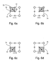
- Figs. 6a, 6b, 6c, 6d show deflection unit vectors.
- Fig. 7 shows deflection assignments at the parent grid pixels.
- Fig. 8 shows image intensity versus distance for the dose modulation technique used alone.
- Fig. 9 illustrates a feature written using dose modulation technique showing edge contour intensities.
- Fig. 10 shows image intensity versus distance for the combination of the dose modulation and deflection.
- Fig. 11 illustrates a feature written using the combination of the dose modulation and deflection techniques.
- Fig. 12 illustrates pictorially a mask or IC feature written using dose modulation and pixel deflection.
- Figs. 13a, 13b, 13c show pictorially a slanted edge of a mask or IC feature with respectively conventional writing, dose modulation, and dose modulation with pixel deflection.
- the current delivered to the substrate to be written to (imaged) is fixed at a certain level and is only changed with a new pattern data file defining a new mask or die or between writing passes.
- dose modulation in accordance with the invention is useful for proximity effect correction and optical proximity correction where the feature to be written has edges which require biasing in order to maintain a uniform line width, i.e. the edges of the feature do not lie along the boundaries halfway between adjacent pixels.
- the beam blanker control electronics are modified to include pulse timing delays determined by a tappable delay line, the selection of the amount of delay being under computer control (called an "autotap") so that the edges of the blanking control pulses are moved in time (and hence space) relative to the raster grid to minimize the X-axis versus Y-axis critical dimensions of the written images.
- autotap pulse timing delays determined by a tappable delay line
- the selection of the amount of delay being under computer control
- the blanker electronics which effectively turn the electron (or other) beam on and off are driven by a control pulse as illustrated in Fig. 1.
- the pulse When the pulse is high this deactivates the blanker to define (illuminate) a pixel on the medium to be written to.
- the horizontal axis represents time t, and the pulse has a nominal width (duration) of X which is inversely proportional to the writing rate.
- a nominal width (duration) of X which is inversely proportional to the writing rate.
- the blanker electronics When a clock pulse of Fig. 1 is received by the blanker electronics, the blanker electronics, in accordance with a second data input signal which controls the pulse duration, delays either or both of the leading or trailing edges of the pulse based on a preset value that the system user determines based on, for instance, experimental data to achieve optimum feature edges.
- the experimentation involves the resist type, process, and dose to make the X vs. Y critical dimensions (CD) the same. Since the X-axis CD is determined by the resist, dose, and process, the only degree of freedom is the Y-axis by controlling the shape width. Alternately, the delays are determined by simulation, or a simple linear approximation of edge placement from the pixel boundaries being proportional to the dose.
- a number of user preset delay values are provided in the pulse blanker control electronics to control the time of occurrence of both the leading and trailing edge of each pixel activation pulse in the blanker electronics. These leading and trailing pulse edges result in a number of preset pulses with varying pulse widths available. This provides a variable dose per pixel.
- the proper pulse width per pixel is selected by modifying the pattern memory in the high speed rasterizer to e.g. a 2 bit (or more) deep bit map representing for example four "gray" levels.
- Fig. 2 where the Data column indicates the two data bits for determining pulse width, i.e. modulating the pulse, and the associated right hand waveforms illustrate the corresponding beam blanker pulse durations varying from nominal 100% duration down to off (0% duration.)
- the intermediate durations 30% and 70% here are examples. The actual values are determined by experimentation to achieve the optimum image result. From signal to noise arguments and the noise characteristics of E-beam gun technology, it has been determined that the number of useful dosage levels is 10 for dosage modulation by itself and 17 for dosage modulation combined with pixel deflection.
- the waveforms of Fig. 2 are achieved in one embodiment by the apparatus of Fig. 3, which allows the user to select the desired beam blanker pulse duration per pixel.
- the blanker control electronics include a data control section 20 which receives both a conventional clock signal determining the writing rate and in this case a D0 and a D1 (extendable to DN) signal, which are the number N data bits shown in the left hand column in Fig. 2.
- the blanker electronics also includes three (N-1) sets of pulse generators 22, 24, 26 (here also labelled pulse 1, pulse 2 and pulse 3). Each set of pulse generators has two controls, one for the pulse leading edge and one for the pulse trailing edge. Each pulse generator 22, 24, 26 can be addressed separately by the data control section 20. The user sets each pulse generator 22, 24, 26 in accordance with the best results taken from experiments for his particular E-beam machine, photoresist medium, and other relevant process factors (or alternatively by simulation or linear approximation).
- the input DIGITAL CLK signal drives all three pulse generator sets 22, 24, 26 as shown thus allowing stable pulses at all times. Selection of which pulse width will be used for a particular pixel is done by a circuit (not shown) which delivers the two bits of data D0, D1 to data control section 20 along with the blanker clock signal.
- the pattern memory in the high speed rasterizer is duplicated as compared to conventional practice to provide the two bit deep memory storing data D0, D1 indicating the pulse width for each pixel.
- the system computer programs (otherwise conventional) are modified (in a manner apparent to one of ordinary skill in the art in accordance with this description) to support this procedure.
- the durations of each of the three pulse widths for pulse 1, pulse 2 and pulse 3 are variable and are determined by the user by providing tappable delay line data via lines 30 to the tappable delay line latches 34 which in turn communicate the duration of the particular pulse needed to the three sets of pulse generators 22, 24, 26. Also provided is a select control signal and a digital clock signal to the tappable delay line latches 34, to load the desired pulse width information in each latch.
- each of the three pulse generators 22, 24, 26 are provided to a high speed pulse select circuit 40 which delivers the appropriate pulse to the beam as needed.
- the pulse select circuit 40 then in response to the clock signal and the two data signals D0, D1 from data control section 20 selects which of the three sets of delay pulses will be provided to the output amplifier 44 which in turn drives the blanking plates (not shown) in the conventional blanker.
- FIG. 4a A typical feature written using dose modulation is numerically represented in Fig. 4a, where the small X's denote intersections of the perimeter lines (light horizontal and vertical lines) defining the pixels.
- the dose value of each pixel is shown digitally in accordance with Fig. 2.
- the heavy line 50 is the outline of the desired feature.
- the left edge 52 of the feature is placed by setting the dose for that column of pixels at 30% (01) and the right edge 54 determined by the 70% dose pixels (10).
- the left edge 52 is spaced approximately 1/3 of the way from the nearest adjacent right grid perimeter line 60
- the right edge 54 of the feature is spaced approximately 2/3 of the way from the nearest adjacent left grid perimeter line 62.
- edges 52, 54 to the feature which lie between the cartesian grid perimeter lines of the raster.
- FIG. 4b Another depiction of the feature of Fig. 4a is shown in Fig. 4b where the relative image intensity of each pixel is shown as the pixel diameter.
- the pixels (circles) are shown centered on the raster grid center points.
- Figures 3, 4a, 4b are representations of the pattern data in the pattern memory. It is to be understood that in reality, where pixel modulation is achieved by controlling pixel exposure (dwell) time, the actual pixel images would be of normal size (beam diameter) in the direction perpendicular to the scan, and shorter in the direction of the scan. Thus in Fig. 4b, the pixels of the left edge 52 are very small (30% of normal), and then at the right edge 54 and somewhat small (70% of normal). The resulting feature outlines as shown.
- the above described dose modulation can be used in accordance with a stripe butting approach for adjacent stripes which form one feature using stripe overlapping, where the overlap area is for example 1/3 to 2/3 dosed in accordance with the present invention.
- This will have the benefits of the well known scan offset voting without the overhead (repeated passes) associated with writing the entire pattern area multiple times. See copending and commonly assigned U.S. patent application Serial No. 08/069-268, filed May 28, 1993 entitled “Gray Scaled Dosing for Lithography” invented by John Poo et al., Attorney Docket No.M-2452.
- a feature written using one embodiment of pixel deflection is illustrated in Figure 5.
- the pixels in the interior 72 and righthand 74 portion of the feature outlined by line 70 are located at the normal raster cartesian grid points. However, the pixels located along the left edge of the feature are deflected (moved) from the normal grid points rightwards by a variable amount so as to define the left edge of the feature to lie off the normal raster grid.
- the pixels in the upper portion 78 of the left edge are deflected less than are the pixels in the lower portion 80 thereof.
- This pixel deflection thereby achieves the advantages of dose modulation, without the need to change the pixel exposure durations.
- the E-beam effective current does not have to be modulated with pixel deflection alone.
- Pixel deflection can be done in one (x,y) direction, with reduced effectiveness, or in both directions.
- the implementation of deflection for the two directions can be different.
- the deflection can be achieved with turn-on and turn-off modulation alone, rather than by electrostatic beam deflection.
- pixel deflection is achieved by a particular type of pattern processing for raster scanning.
- the design pattern defining the feature is composed at an address unit of one half of the writing address unit (the normal cartesian grid spacing).
- the address unit size is doubled, to its normal size.
- the relation of the design pixel (child) and the writing pixel (parent) is shown in Figs. 6a, 6b, 6c, 6d where the circles are the corner points of the parents and the crosses are the children.
- Figs. 6a, 6b, 6c, 6d display the same parent pixel, but highlighting a different child pixel. At each parent pixel, e.g.
- the vector sum (arrows) of the intersecting child pixels 73, 75, 77, 79 is calculated.
- the coordinate pairs, e.g. (-1, 1) represent the four unit vectors of deflection. This sum is mapped into the intensity value at which the pixel is exposed (as described below). For pixel deflection used without dose modulation, this intensity value is the full pixel intensity value.
- the direction of the deflection is given by the direction of the vector sum of the constituent child pixels interacting with the parent.
- the amplitude of the deflection is a function of the sum of the number of constituent child pixels and possibly the pixel configuration. Additional improvements to the positioning of the pixel could be done, if the arrangement of the neighboring pixels is considered.
- the needed deflection is typically inversely related to the sum of the number of constituent configuration.
- An example of a feature pattern defined by outline 80 and the corresponding deflection of each parent is shown in Fig. 7. As shown here, the left 82 and top 84 edges of the feature 80 are extended beyond the parent pixels, e.g. pixel 86, by 1/2 of the writing address unit to the adjacent child pixel 88.
- a generalization of the deflection method allows calculation of the overlap area of the parent pixel with angled lines and assigns a displacement corresponding to the overlap area and assigns a location of the parent pixel. This allows elimination of the staircase effect for angled feature edges than one might obtain for instance with dose modulation.
- Pixel deflection is used during writing of feature edge pixels in the x direction and may be used in the y (scan) direction as explained below.
- the maximum deflection typically is one half pixel length in any direction, and adjacent pixels may have different deflection amounts.
- the precision of the deflection is dependent on the number of edge placements that are used; one example would be sixteen edge placements for each pixel in each direction; i.e., 32 displacement gradations between normal pixel centers.
- Edge deflection is achieved in an E-beam system in terms of apparatus by an electrostatic beam deflector which is impedance matched to the deflector driving circuit.
- each deflector includes an offset (off axis) hole drilled all the way through a coaxial transmission line. The electron beam passes through the hole and is deflected by a voltage of particular levels (plus or negative) on the transmission line central conductor; the outer conductor is at ground.
- One such deflector is provided for each axis (X,Y) in which deflection is to take place.
- Other electrostatic deflectors are also suitable. These X and Y deflectors are placed in the objective lens of the electron beam system.
- Deflection is performed during writing at the start of scan of the beam across a particular pixel. It must be possible to turn the deflection on or off in a time comparable to the write time of a typical feature, usually many pixels in duration. Thus one can start the deflection gradually on pixels that are not written, and turn it off gradually over several pixels that are being written. Typical values for the magnitude of the deflection would be 0, 0.05, 0.07 and 0.1 micrometers for a 0.1 micrometer diameter address unit (pixel diameter).
- Pulse offsets eliminate the need for the Y-direction deflector by instead advancing or delaying the writing pulse that actuate the beam blanker during scanning; this shifts the pulse center left or right of its normal position.
- tappable delay lines advance or delay (in time and hence space) the pixel writing pulse by a predetermined amount.
- Fig. 8 shows image intensity (vertical axis) versus distance ( ⁇ m) from an arbitrary vertical line to a vertical feature edge for dose modulation, given a four pixel wide line (and assuming scanning in the Y-direction). Varying doses of 0%, 33%, 66% and 100% of the maximum dose correspond respectively to index numbers 1, 2, 3, and 4 for address unit and beam diameter of 0.1 micron. Note that the edge profile changes dramatically as the dose at the edge is varied. This is a significant deficiency.
- Fig. 9 shows the equal intensity contours 100 of exposure distribution resulting from writing a feature test pattern 104 as shown, where the dose is varied as in Fig.8 at the left edge of the feature. Note that the horizontal distance between contours increases as the dose at the edge pixels is decreased (bottom to top of feature 104). This may result in reduced process latitude.
- Fig. 10 shows image intensity versus distance for a four pixel wide line (assuming scanning the y direction) with both dose modulation and pixel deflection as indicated in Table 1 for four combinations of dose and deflection. Note that the edge profile does not change as the edge is displaced. Displacement is measured from the edge of the neighboring pixel. (For Figs. 10 and 11) Index Displacement Dose Shift (in Linewidth) 1 0 0 0% 2 .05 33% 0.0238 3 .03 66% 0.0561 4 0 100% 0.1
- Fig. 11 shows the corresponding equal intensity contours of the exposure distributions resulting from writing the feature test pattern 104 shown using dose modulation and pixel deflection corresponding to Figure 10.
- the horizontal distance between contours 108 at the left edge of the figure is approximately constant, because the edge is displaced. This desirably results in uniform process latitude.
- Fig. 12 Details of a feature written using combined dose modulation and pixel deflection is shown in Fig. 12 note that the pixels at the left edge 116 of the feature 114 (defined by outline 118) are both of reduced size and shifted off the normal grid centerpoints.
- dose modulation is accomplished in the same manner as in dose modulation used by itself.
- Figs. 13a, 13b, 13c show pictorially a triangular feature 122 written respectively using conventional single pass printing, dose modulation by itself, and dose modulation with pixel deflection.
- the pixels here are represented as contiguous squares. The darker pixels are those with more intense doses.
- the perceived edges of each feature 122 is delineated by a line; line 124 of Fig. 13a is non-uniform (uneven).
- Line 126 of Fig. 13b is closer to the original triangle shape.
- Line 128 of Fig. 13c is even closer to the original triangle shape, with better uniformity.
Landscapes
- Chemical & Material Sciences (AREA)
- Engineering & Computer Science (AREA)
- Nanotechnology (AREA)
- Analytical Chemistry (AREA)
- Crystallography & Structural Chemistry (AREA)
- Physics & Mathematics (AREA)
- Theoretical Computer Science (AREA)
- Mathematical Physics (AREA)
- Condensed Matter Physics & Semiconductors (AREA)
- General Physics & Mathematics (AREA)
- Manufacturing & Machinery (AREA)
- Electron Beam Exposure (AREA)
- Exposure And Positioning Against Photoresist Photosensitive Materials (AREA)
Abstract
Description
- This invention relates to raster scan lithography as used for producing masks and wafers for integrated circuit fabrication, and more specifically to raster scan electron beam systems.
- It is well known to use particle (electron or ion) or light beam exposure systems for the manufacture of microminiature electronic devices (integrated circuits). Often these systems use raster scan beam lithography methods. Such lithographic employing a controllable electron beam, sometimes called E-beam machines, for fabrication of integrated circuits are well known; one such system is described in U.S. Patent No. 3,900,737 to Collier et al. and an other in U.S. Patent No. 3,801,792 to Lin.
- In these machines a medium of resist (or photosensitive) material upon which the electron beam is to perform its writing operation is provided overlying a substrate which is to become a mask for imaging a wafer or which is the wafer itself (direct writing). The medium with its underlying substrate is positioned on a motordriven stage which is moved continuously in synchronism as the beam is scanned in a raster fashion (a raster scan) and in a direction perpendicular to the stage motion. In practice, the diameter of the round electron beam spot, also called a "Gaussian spot" or "pixel", focussed on the resist layer, is of the order of (but not necessarily equal to) the writing address dimension (or address unit) of the cartesian grid on which it is written. Adjacent rows of pixels in the stage travel direction define the width of a "feature" and a length of the feature is formed by a number of pixels in the raster scan direction. The feature is for instance an element of the integrated circuit such as a conductive interconnect or a portion of a transistor. In practice, adjacent "on" pixels in the same raster scan are not separately scanned; instead the beam is kept on until an "off" pixel is encountered. For the purposes of this disclosure, descriptions are given in terms of the normal full pixelization representation. The turning on and off of the beam is achieved by a beam blanker which is a well known portion of an E-beam machine, one example of which is shown in U.S. Patent No. 5,276,330, patent application serial no. 07/706,612, filed May 29, 1991, entitled 'High Accuracy Beam Blanker" incorporated by reference herein, invented by Mark A. Gesley. The pattern on the resist defined by the beam scan and by the stage movement is determined by the system control equipment which includes certain computer software programs.
- Several modifications of this system are used to achieve feature edge position increment which is finer than the raster grid, i.e. the edges of a feature fall between the center points of the cartesian grid defined by the pixel centerpoints. One example of such a system is described in Berglund et al., U.S. Patent No. 5,103,101 incorporated by reference and defining a system for multiphase printing for E-beam lithography. Another such system is described in U.S. Patent No. 4,879,605 to Warkentin et al. for a rasterizing system using an overlay of bit map low address resolution databases, using a multi-pass laser beam writing technique to vary the dosage at a feature edge dependent upon the desired location of a given edge.
- Another relevant disclosure is U.S. Patent No. 4,498,010 to Biechler et al. which provides a virtual addressing technique and is incorporated by reference.
- The above disclosures are directed to raster scan methods using a bit map of an image of the feature to be written, in which each pixel is typically either on or off. In contrast, in vector scan lithographic machines, shapes are defined in a stored image. It is well known in vector scan machines to alter the dosage (intensity) of a particular shape.
- However the above referenced prior art does not provide, in the context of raster scan, a method for defining an edge of a feature to lie between pixel centers, i.e. to move the edge of the feature off the pixel grid, except by (1) use of multi-scan passes or (2) using virtual addressing to turn complete pixels on or off, producing unwanted edge roughness and pattern distortion. Each such pass requires a significant amount of time and hence reduces throughput of a raster scan machine, thus increasing the cost of the masks or integrated circuits formed thereby.
- Warkentin et al. discloses in Fig. 7b (see col. 5, beginning at line 49):
- By reducing the dosage of the light source as shown by graph 708, only desired area 705 is exposed to the exposure threshold level 703(b).
- Figure 7b shows the edge of a feature 702(b) in which the dosage of the laser beam source is reduced (modulated) for area 705 of the image. Warkentin et al. changes dose by reducing laser intensity.
- Moreover, Warkentin et al. does not indicate that such an approach is suitable, and instead teaches the approach as shown in their Fig. 7c in which the level dose is reduced for all pixels exposed in one pass which are therefore of uniform intensity. Multiple passes of the beams, i.e., multiple scans, are used (see col. 5,
lines 54 through 58). Thus, Warkentin et al. teach a multi-pass system with the attendant reduction in throughput. - "Patent Abstracts of Japan," Vol. 11, No. 363 (E-560), November 26, 1987, corresponding to JP 62137824A, June 20, 1987, and "Patent Abstracts of Japan," Vol. 11, No. 286 (E-541), September 16, 1987, corresponding to JP 62086717A, April 21, 1987, disclose a method having the features of the preamble of
claim 1. - It is the object of the invention to provide an improved method of exposing a medium which is sensitive to exposure from a beam in a raster scan lithography apparatus and a corresponding raster scan photolithography apparatus.
- These objects are achieved with a method having the features of
claim 1 and an apparatus having the features of claim 14. - Three methods and associated apparatuses each achieve a finer effectual grid size than the actual writing grid of a raster scan system:
- 1) Pixel intensity (dose) modulation through blanker pulse width modulation, according to the invention.
- 2) Sub-pixel deflection for modulating feature edge position.
- 3) A combination of inventive dose modulation and sub-pixel deflection to optimize the integrity of the written pattern and minimize the disadvantages of dose modulation and pixel deflection.
-
- For a raster scan lithography system, the capability is provided to set (modulate) the dose of individual pixels to a known level on the fly on a pixel-by-pixel basis using pulse-width modulation at high speed, for the purpose of moving an edge of an image feature away from the pixel center-to-center cartesian grid. This is achieved using pulse-width modulation without reducing the beam current density. (Reducing current density is problematic for E-beams).
- This is done in a single pass scan by selectively reducing the duration of the pulses defining the individual pixel duration. In one embodiment this is accomplished by adding circuitry to the beam blanker control electronics which provides a number of preset delay values for both the leading and trailing edge of the pulses defining the duration of each pixel. (These pulse edges are not to be confused with the feature edges). These leading and trailing pulse edge delays result in a number of preset pulses with varying pulse widths, providing a variable (modulated) dose per pixel.
- In accordance with one embodiment of the invention, in addition to the conventional 100% "full" duration pixel representing a full dose, and the conventional 0% duration representing absence of an exposed pixel, two additional user definable pixel dose levels are provided, e.g. one being about 30% of the duration of nominal and the second being about 70% of the duration of nominal. Thus, a set of delay elements in the beam blanker control electronics are activated by e.g. a two bit data signal associated with each pixel indicating which of the four pixel durations (0%, 30%, 70% or 100%) are to be assigned to each pixel.
- Advantageously, this method is applicable to the prior art multi-phase printing and virtual addressing systems described above. In accordance with one application of the present invention, the pixel dose modulation is somewhat similar in result in terms of the written feature to the above described virtual addressing, in that the writing of the image can be done on an address grid three times as large as the design grid by using the two additional modulated dose levels. Thus, the edges of the written feature that fall at about 1/3 or 2/3 of the writing cartesian grid are exposed respectively for instance at 30% pulse duration of nominal or 70% pulse duration of nominal. This approach provides a feature having the high definition of normal raster scan printing with a nine times improvement in throughput, since one can use a three times larger writing grid than is required in the prior art. The same advantage obtains over the multi-phase printing process wherein the medium must be exposed in four passes (the stage travel is repeated three times). Additionally, the method in accordance with the invention minimizes edge roughness of the written feature, compared to virtual addressing which has a characteristic undesirable edge roughness artifact. Advantageously, beam size does not need to be expanded, since there are no "missing" pixels unlike the case with virtual addressing. Additionally, the dose modulation method in accordance with the invention minimizes corner rounding of features commensurately with address unit used during writing, unlike the prior art methods.
- In an example of the throughput advantage of dose modulation for a typical mask for a 256 Mbit DRAM integrated circuit (IC) at a 0.025 micrometer address grid, a typical chip size is 70x125 millimeters. Thus the number of pixels is 1.4 x 10¹³ for one IC die. At a 320 MHz pixel rate, the exposure time is thus 12 hours for one pass writing at 1 Hz/pixel. However, dose modulation reduces this exposure time to 1.3 hours assuming three dosage modulation levels.
- In the following, a method useful in understanding the present invention is described.
- The method in the context of raster scan lithography for defining an edge of a feature to lie between pixel centers, i.e. to move the edge of the feature off the pixel grid, does so directly during pixel writing by deflecting the beam so that the pixel centers are displaced by a variably preselected amount from the normal pixel grid center positions. Pixel deflection is typically limited to less than plus and minus one-half of an address unit. In one example the various displacement amounts are equal to the address unit (the nominal pixel diameter), 70% of the address unit, 50% of the address unit, and the conventional zero displacement. This deflection of the actual pixel locations achieves some of the same advantages as described above for dose modulation such as reducing corner rounding. Thus the position of the pattern edges, i.e. feature edges, is changed directly relative to the raster grid.
- Pixel deflection allows feature edge positions to be moved in increments less than the address grid. However, in doing so there is an effective dose modulation, because adjacent pixels overlap their intensities differently when their spacings are changed. If uncorrected this results in error in edge position and/or degradation of process latitude. This problem can be corrected in several ways combining dose modulation and deflection, but other schemes such as deflecting all pixels within three or four pixel spacings of the edge exactly the same amount are applicable.
- Pixel deflection is achieved in one version by deflecting only along the X direction in the scan (the scan conventionally defining both X and Y directions) with a maximum deflection of one-half pixel length. More generally the deflection is in both the X and Y directions. Adjacent pixels may have different deflection amounts depending on the feature edge position needed. An apparatus for achieving deflection is to use two matched impedance electrostatic beam deflectors (one for each deflection direction X and Y) in an E-beam raster scanning system. Thus the objective lens portion of the system is modified to provide for the needed pixel deflection, under computer control.
- Pixel deflection may also be used in combination with dose modulation, whereby particular pixels are modified both by (1) having less than 100% of the maximum dose and (2) having their centers deflected from the normal position. The combination is especially advantageous in providing better definition of feature edges, including achieving symmetrical corner rounding independent of corner position relative to nominal pixel centers while maintaining process latitude. (Process latitude refers to change in line width or edge position due to dose variation, or development time variation) This approach therefore maintains the steepness and integrity of the edge dose profile versus position, independent of feature edge position relative to nominal address grid.
- Fig. 1 shows an ideal control pulse waveform for the blanker electronics of a raster scan E-beam photolithography machine.
- Fig. 2 shows wave forms illustrating various modulated beam blanker pulse widths in accordance with dose modulation.
- Fig. 3 shows control electronics in block form for beam blanker electronics for dose modulation.
- Fig. 4a illustrates numerically a mask or IC feature written using dose modulation.
- Fig. 4b illustrates pictorially a mask or IC feature written using dose modulation.
- Fig. 5 illustrates pictorially a mask or IC feature written using pixel deflection.
- Figs. 6a, 6b, 6c, 6d show deflection unit vectors.
- Fig. 7 shows deflection assignments at the parent grid pixels.
- Fig. 8 shows image intensity versus distance for the dose modulation technique used alone.
- Fig. 9 illustrates a feature written using dose modulation technique showing edge contour intensities.
- Fig. 10 shows image intensity versus distance for the combination of the dose modulation and deflection.
- Fig. 11 illustrates a feature written using the combination of the dose modulation and deflection techniques.
- Fig. 12 illustrates pictorially a mask or IC feature written using dose modulation and pixel deflection.
- Figs. 13a, 13b, 13c show pictorially a slanted edge of a mask or IC feature with respectively conventional writing, dose modulation, and dose modulation with pixel deflection.
- Typically in raster scan electron beam photolithography machines (and also those using other types of beams, such as light or ions) the current delivered to the substrate to be written to (imaged) is fixed at a certain level and is only changed with a new pattern data file defining a new mask or die or between writing passes. As described above, dose modulation in accordance with the invention is useful for proximity effect correction and optical proximity correction where the feature to be written has edges which require biasing in order to maintain a uniform line width, i.e. the edges of the feature do not lie along the boundaries halfway between adjacent pixels.
- Therefore, in accordance with the invention the beam blanker control electronics are modified to include pulse timing delays determined by a tappable delay line, the selection of the amount of delay being under computer control (called an "autotap") so that the edges of the blanking control pulses are moved in time (and hence space) relative to the raster grid to minimize the X-axis versus Y-axis critical dimensions of the written images. Thus, one achieves variable pulse widths for each pixel on a selective basis in order to control the pixel dose, i.e. the amount of irradiation or particles impacting on the substrate anywhere within the scan pattern maintained by a high speed rasterizer (a raster engine where the bit map representation of the feature or pattern is stored prior to the exposure).
- As is conventional, the blanker electronics which effectively turn the electron (or other) beam on and off are driven by a control pulse as illustrated in Fig. 1. When the pulse is high this deactivates the blanker to define (illuminate) a pixel on the medium to be written to. The horizontal axis represents time t, and the pulse has a nominal width (duration) of X which is inversely proportional to the writing rate. Thus, for a writing rate of 40 MHz the value of X is 25 nanoseconds, for 80 MHz rate the value of X is 12.5 nanoseconds, and for 160 MHz rate the value of X is 6.25 nanoseconds.
- When a clock pulse of Fig. 1 is received by the blanker electronics, the blanker electronics, in accordance with a second data input signal which controls the pulse duration, delays either or both of the leading or trailing edges of the pulse based on a preset value that the system user determines based on, for instance, experimental data to achieve optimum feature edges. The experimentation involves the resist type, process, and dose to make the X vs. Y critical dimensions (CD) the same. Since the X-axis CD is determined by the resist, dose, and process, the only degree of freedom is the Y-axis by controlling the shape width. Alternately, the delays are determined by simulation, or a simple linear approximation of edge placement from the pixel boundaries being proportional to the dose.
- Therefore, a number of user preset delay values are provided in the pulse blanker control electronics to control the time of occurrence of both the leading and trailing edge of each pixel activation pulse in the blanker electronics. These leading and trailing pulse edges result in a number of preset pulses with varying pulse widths available. This provides a variable dose per pixel. The proper pulse width per pixel is selected by modifying the pattern memory in the high speed rasterizer to e.g. a 2 bit (or more) deep bit map representing for example four "gray" levels.
- This is illustrated in Fig. 2 where the Data column indicates the two data bits for determining pulse width, i.e. modulating the pulse, and the associated right hand waveforms illustrate the corresponding beam blanker pulse durations varying from nominal 100% duration down to off (0% duration.) The
intermediate durations 30% and 70% here are examples. The actual values are determined by experimentation to achieve the optimum image result. From signal to noise arguments and the noise characteristics of E-beam gun technology, it has been determined that the number of useful dosage levels is 10 for dosage modulation by itself and 17 for dosage modulation combined with pixel deflection. - The waveforms of Fig. 2 are achieved in one embodiment by the apparatus of Fig. 3, which allows the user to select the desired beam blanker pulse duration per pixel. The blanker control electronics include a
data control section 20 which receives both a conventional clock signal determining the writing rate and in this case a D0 and a D1 (extendable to DN) signal, which are the number N data bits shown in the left hand column in Fig. 2. The blanker electronics also includes three (N-1) sets ofpulse generators pulse 1,pulse 2 and pulse 3). Each set of pulse generators has two controls, one for the pulse leading edge and one for the pulse trailing edge. Eachpulse generator data control section 20. The user sets eachpulse generator - The input DIGITAL CLK signal drives all three pulse generator sets 22, 24, 26 as shown thus allowing stable pulses at all times. Selection of which pulse width will be used for a particular pixel is done by a circuit (not shown) which delivers the two bits of data D0, D1 to
data control section 20 along with the blanker clock signal. - Thus the pattern memory in the high speed rasterizer is duplicated as compared to conventional practice to provide the two bit deep memory storing data D0, D1 indicating the pulse width for each pixel. The system computer programs (otherwise conventional) are modified (in a manner apparent to one of ordinary skill in the art in accordance with this description) to support this procedure.
- As shown in Fig. 3, the durations of each of the three pulse widths for
pulse 1,pulse 2 andpulse 3 are variable and are determined by the user by providing tappable delay line data vialines 30 to the tappable delay line latches 34 which in turn communicate the duration of the particular pulse needed to the three sets ofpulse generators - The outputs of each of the three
pulse generators select circuit 40 which delivers the appropriate pulse to the beam as needed. The pulseselect circuit 40 then in response to the clock signal and the two data signals D0, D1 fromdata control section 20 selects which of the three sets of delay pulses will be provided to theoutput amplifier 44 which in turn drives the blanking plates (not shown) in the conventional blanker. - It will be understood that other circuitry will also provide dose modulation in accordance with the invention.
- A typical feature written using dose modulation is numerically represented in Fig. 4a, where the small X's denote intersections of the perimeter lines (light horizontal and vertical lines) defining the pixels. The dose value of each pixel is shown digitally in accordance with Fig. 2. The
heavy line 50 is the outline of the desired feature. Note that theleft edge 52 of the feature is placed by setting the dose for that column of pixels at 30% (01) and theright edge 54 determined by the 70% dose pixels (10). Thus theleft edge 52 is spaced approximately 1/3 of the way from the nearest adjacent rightgrid perimeter line 60, and theright edge 54 of the feature is spaced approximately 2/3 of the way from the nearest adjacent leftgrid perimeter line 62. Thus, one has provided well definededges - Another depiction of the feature of Fig. 4a is shown in Fig. 4b where the relative image intensity of each pixel is shown as the pixel diameter. In Fig. 4b the pixels (circles) are shown centered on the raster grid center points. Also, Figures 3, 4a, 4b are representations of the pattern data in the pattern memory. It is to be understood that in reality, where pixel modulation is achieved by controlling pixel exposure (dwell) time, the actual pixel images would be of normal size (beam diameter) in the direction perpendicular to the scan, and shorter in the direction of the scan. Thus in Fig. 4b, the pixels of the
left edge 52 are very small (30% of normal), and then at theright edge 54 and somewhat small (70% of normal). The resulting feature outlines as shown. - The above described dose modulation can be used in accordance with a stripe butting approach for adjacent stripes which form one feature using stripe overlapping, where the overlap area is for example 1/3 to 2/3 dosed in accordance with the present invention. This will have the benefits of the well known scan offset voting without the overhead (repeated passes) associated with writing the entire pattern area multiple times. See copending and commonly assigned U.S. patent application Serial No. 08/069-268, filed May 28, 1993 entitled "Gray Scaled Dosing for Lithography" invented by John Poo et al., Attorney Docket No.M-2452.
- A feature written using one embodiment of pixel deflection is illustrated in Figure 5. The pixels in the interior 72 and righthand 74 portion of the feature outlined by
line 70 are located at the normal raster cartesian grid points. However, the pixels located along the left edge of the feature are deflected (moved) from the normal grid points rightwards by a variable amount so as to define the left edge of the feature to lie off the normal raster grid. The pixels in theupper portion 78 of the left edge are deflected less than are the pixels in thelower portion 80 thereof. This pixel deflection thereby achieves the advantages of dose modulation, without the need to change the pixel exposure durations. Advantageously the E-beam effective current does not have to be modulated with pixel deflection alone. - It is to be understood that in other embodiments, one would displace all pixels linearly from one edge of a feature toward its opposite edge. Also, in yet another embodiment one would displace N adjacent pixels near each edge exactly the same amount, where N = 2, 3, or 4 for example.
- Pixel deflection can be done in one (x,y) direction, with reduced effectiveness, or in both directions. The implementation of deflection for the two directions can be different. For example, in the scan direction the deflection can be achieved with turn-on and turn-off modulation alone, rather than by electrostatic beam deflection.
- In one embodiment, pixel deflection is achieved by a particular type of pattern processing for raster scanning. For data processing purposes, the design pattern defining the feature is composed at an address unit of one half of the writing address unit (the normal cartesian grid spacing). For the actual writing process, the address unit size is doubled, to its normal size. The relation of the design pixel (child) and the writing pixel (parent) is shown in Figs. 6a, 6b, 6c, 6d where the circles are the corner points of the parents and the crosses are the children. Each of Figs. 6a, 6b, 6c, 6d display the same parent pixel, but highlighting a different child pixel. At each parent pixel,
e.g. pixel 71, the vector sum (arrows) of the intersectingchild pixels - The amplitude of the deflection is a function of the sum of the number of constituent child pixels and possibly the pixel configuration. Additional improvements to the positioning of the pixel could be done, if the arrangement of the neighboring pixels is considered. The needed deflection is typically inversely related to the sum of the number of constituent configuration. An example of a feature pattern defined by
outline 80 and the corresponding deflection of each parent is shown in Fig. 7. As shown here, the left 82 and top 84 edges of thefeature 80 are extended beyond the parent pixels,e.g. pixel 86, by 1/2 of the writing address unit to theadjacent child pixel 88. - A generalization of the deflection method allows calculation of the overlap area of the parent pixel with angled lines and assigns a displacement corresponding to the overlap area and assigns a location of the parent pixel. This allows elimination of the staircase effect for angled feature edges than one might obtain for instance with dose modulation.
- The reduction in or decoupling of the allowable feature edge increment from that of the address grid is a particular implementation here. Benefits can also be achieved for this method by keeping the original grid and using the pixel deflection technique to reduce critical dimension variation on angled feature edges, or using edge smoothing algorithms (such as computer graphics antialiasing algorithm) at feature edges as is well known in the art.
- Pixel deflection is used during writing of feature edge pixels in the x direction and may be used in the y (scan) direction as explained below. The maximum deflection typically is one half pixel length in any direction, and adjacent pixels may have different deflection amounts. The precision of the deflection is dependent on the number of edge placements that are used; one example would be sixteen edge placements for each pixel in each direction; i.e., 32 displacement gradations between normal pixel centers.
- Edge deflection is achieved in an E-beam system in terms of apparatus by an electrostatic beam deflector which is impedance matched to the deflector driving circuit. In one embodiment each deflector includes an offset (off axis) hole drilled all the way through a coaxial transmission line. The electron beam passes through the hole and is deflected by a voltage of particular levels (plus or negative) on the transmission line central conductor; the outer conductor is at ground. One such deflector is provided for each axis (X,Y) in which deflection is to take place. Other electrostatic deflectors are also suitable. These X and Y deflectors are placed in the objective lens of the electron beam system.
- Deflection is performed during writing at the start of scan of the beam across a particular pixel. It must be possible to turn the deflection on or off in a time comparable to the write time of a typical feature, usually many pixels in duration. Thus one can start the deflection gradually on pixels that are not written, and turn it off gradually over several pixels that are being written. Typical values for the magnitude of the deflection would be 0, 0.05, 0.07 and 0.1 micrometers for a 0.1 micrometer diameter address unit (pixel diameter).
- An alternative method of achieving a kind of deflection in the Y direction is to use pulse offsets. Pulse offsets eliminate the need for the Y-direction deflector by instead advancing or delaying the writing pulse that actuate the beam blanker during scanning; this shifts the pulse center left or right of its normal position. Thus tappable delay lines (in addition to those described above in conjunction with dose modulation) advance or delay (in time and hence space) the pixel writing pulse by a predetermined amount.
- The combination of pixel deflection with dose modulation preserves the constant dose density. Moving a pixel's position relative to its nearest neighbors changes the combined dose that occurs in the vicinity of the moved (deflected) pixels. This change in local dose can be compensated for by adding (minor) pixel dose modulation to the deflected pixels, thus achieving the advantages of both pixel deflection and dose modulation. Thus total exposure dose per pattern is constant while maintaining pattern edge slope integrity. Thus process latitude is not adversely affected.
- Fig. 8 shows image intensity (vertical axis) versus distance (µm) from an arbitrary vertical line to a vertical feature edge for dose modulation, given a four pixel wide line (and assuming scanning in the Y-direction). Varying doses of 0%, 33%, 66% and 100% of the maximum dose correspond respectively to
index numbers equal intensity contours 100 of exposure distribution resulting from writing afeature test pattern 104 as shown, where the dose is varied as in Fig.8 at the left edge of the feature. Note that the horizontal distance between contours increases as the dose at the edge pixels is decreased (bottom to top of feature 104). This may result in reduced process latitude. - Fig. 10 shows image intensity versus distance for a four pixel wide line (assuming scanning the y direction) with both dose modulation and pixel deflection as indicated in Table 1 for four combinations of dose and deflection. Note that the edge profile does not change as the edge is displaced. Displacement is measured from the edge of the neighboring pixel.
(For Figs. 10 and 11) Index Displacement Dose Shift (in Linewidth) 1 0 0 0% 2 .05 33% 0.0238 3 .03 66% 0.0561 4 0 100% 0.1 - The Shift value in Table 1 was determined empirically.
- Fig. 11 shows the corresponding equal intensity contours of the exposure distributions resulting from writing the
feature test pattern 104 shown using dose modulation and pixel deflection corresponding to Figure 10. The horizontal distance betweencontours 108 at the left edge of the figure is approximately constant, because the edge is displaced. This desirably results in uniform process latitude. - Details of a feature written using combined dose modulation and pixel deflection is shown in Fig. 12 note that the pixels at the
left edge 116 of the feature 114 (defined by outline 118) are both of reduced size and shifted off the normal grid centerpoints. In the combined deflection and dose modulation technique, dose modulation is accomplished in the same manner as in dose modulation used by itself. - For a further illustration, Figs. 13a, 13b, 13c show pictorially a
triangular feature 122 written respectively using conventional single pass printing, dose modulation by itself, and dose modulation with pixel deflection. The pixels here are represented as contiguous squares. The darker pixels are those with more intense doses. As shown, the perceived edges of eachfeature 122 is delineated by a line; line 124 of Fig. 13a is non-uniform (uneven).Line 126 of Fig. 13b is closer to the original triangle shape.Line 128 of Fig. 13c is even closer to the original triangle shape, with better uniformity. - The above description is illustrative and not limiting; further modifications will be apparent to one of ordinary skill in the art and are intended to be encompassed by the appended claims.
Claims (20)
- A method of exposing a medium which is sensitive to exposure from a beam in a raster scan lithography apparatus, comprising the steps of:characterized byscanning the beam across a surface of the medium in a raster pattern, thereby exposing a plurality of pixels of the raster pattern on the medium to form at least one exposed feature on the surface of the medium, the feature including the plurality of the pixels and having at least one edge;modulating a duration of the exposure of at least some of the pixels at the edge of the feature by reducing a duration of the exposure of the pixels at the edge compared to the pixels at other portions of the feature, thereby defining the edge of the feature as a line lying off a grid defined by locations of the pixels of the raster pattern.
- The method of claim 1,
characterized in that
the step of modulating comprises:predetermining at least three durations of the exposure, one of the durations being zero; andselecting one of the at least three durations for each pixel to be exposed. - The method of claim 2,
characterized in that
the step of predetermining comprises:providing a delay circuit having at least two pairs of delays, each having two delays, one delay associated with a beginning, one delay associated with a termination of a particular pixel exposure. - The method of claim 3,
characterized in that
the step of selecting comprises:providing a timing signal and a duration selection signal to a blanker for blanking the beam; andblanking the beam in accordance with the timing signal and the duration selection signal to modulate the duration of the exposure. - The method of claim 4,
characterized in thatthe duration selection signal is a digital signal having at least two digits for each pixel of the plurality of pixels. - The method of claim 2,
characterized by
further comprising providing at least three predetermined durations in addition to zero, the durations being 100%, about 70%, and about 30% of a full pixel exposure duration; and further comprising the steps of:exposing pixels at the about 70% duration for a particular pixel occurring at an edge of the feature located about 2/3 of the way between the particular pixel and an adjacent unexposed pixel; andexposing pixels at the about 30% duration for a particular pixel occurring at an edge of the feature located about 1/3 of the way between the particular pixel and an adjacent unexposed pixel. - The method of any one of the claims 1 to 6,
characterized byfurther comprising the step of deflecting the beam while it is scanning at least some of the pixels at the edge of the feature, thereby locating the pixels at the edge at locations lying off the grid. - The method of claim 7,
characterized in that
the step of deflecting comprises:predetermining at least two amounts of deflection; andselecting one of the at least two amounts for deflecting each of the deflected pixels. - The method of claim 8,
characterized in that
the step of deflecting further comprises:providing an electrostatic beam deflector; andcontrolling a voltage to the electrostatic deflector thereby deflecting the beam. - The method of one of the claims 8 and 9,
characterized byfurther comprising providing at least three amounts of deflection, wherein the at least three amounts of deflection, relative to the center-to-center spacing between undeflected pixels, are respectively about 1/2, 0.35 and 0.25. - The method of claim 7,
characterized in thatthe raster pattern defines two perpendicular directions, and the step of deflecting includes deflecting along only one of the two directions. - The method of claim 11,
characterized byfurther comprising deflecting along the other of the two directions. - The method of claim 7,
characterized byfurther comprising the step of deflecting the beam linearly for all pixels within a feature. - A raster scan photolithography apparatus comprising:characterized bya beam generator;a support for a medium sensitive to exposure from the beam;a raster scanning system located between the beam generator and the support for scanning the beam across the medium in a raster pattern having a plurality of pixels to expose a feature on the surface of the medium defined by some of the pixels;a beam blanker located between the beam generator and the support for blanking the beam, thereby defining the pixels;
a beam blanker controller operatively connected to the beam blanker for reducing a duration of the pixels located at an edge of the feature to at least two predetermined levels each intermediate of a zero duration and a full pixel duration. - The apparatus of claim 14,
characterized by
the beam blanker controller including at least two preset delay paths for reducing the duration of the pixels to the two intermediate levels. - The apparatus of claim 15,
characterized by
the two preset delay paths defining pixel durations of about 30% and about 70% of the full pixel duration. - The apparatus of one of the claims 15 and 16,
characterized by
the beam blanker controller including a data control portion for receiving a data signal having at least two digits for determining which of the preset delay paths reduces each pixel duration. - The apparatus of one of the claims 14 to 17,
characterized by
a two bit deep pattern memory associated with the beam blanker controller for storing data defining the duration of the exposure of each pixel at the edge of the feature. - The method of one of the claims 1 to 13,
characterized in that
the modulation step comprises the variation of the pulse width defining a duration of the pixels. - The method of one of the claims 1 to 13 or 19,
characterized by
further comprising storing data defining the duration of the exposure of each pixel at the edge of the feature in a two bit deep pattern memory.
Applications Claiming Priority (3)
| Application Number | Priority Date | Filing Date | Title |
|---|---|---|---|
| US69222 | 1993-05-28 | ||
| US08/069,222 US5393987A (en) | 1993-05-28 | 1993-05-28 | Dose modulation and pixel deflection for raster scan lithography |
| PCT/US1994/005102 WO1994028574A1 (en) | 1993-05-28 | 1994-05-06 | Dose modulation and pixel deflection for raster scan lithography |
Publications (3)
| Publication Number | Publication Date |
|---|---|
| EP0653103A1 EP0653103A1 (en) | 1995-05-17 |
| EP0653103A4 EP0653103A4 (en) | 1998-12-16 |
| EP0653103B1 true EP0653103B1 (en) | 2001-12-19 |
Family
ID=22087529
Family Applications (1)
| Application Number | Title | Priority Date | Filing Date |
|---|---|---|---|
| EP94917933A Expired - Lifetime EP0653103B1 (en) | 1993-05-28 | 1994-05-06 | Dose modulation and pixel deflection for raster scan lithography |
Country Status (7)
| Country | Link |
|---|---|
| US (1) | US5393987A (en) |
| EP (1) | EP0653103B1 (en) |
| JP (1) | JP3323505B2 (en) |
| KR (1) | KR0174585B1 (en) |
| CA (1) | CA2139637C (en) |
| DE (1) | DE69429498T2 (en) |
| WO (1) | WO1994028574A1 (en) |
Families Citing this family (59)
| Publication number | Priority date | Publication date | Assignee | Title |
|---|---|---|---|---|
| US6274290B1 (en) | 1997-01-28 | 2001-08-14 | Etec Systems, Inc. | Raster scan gaussian beam writing strategy and method for pattern generation |
| US5847959A (en) * | 1997-01-28 | 1998-12-08 | Etec Systems, Inc. | Method and apparatus for run-time correction of proximity effects in pattern generation |
| US5876902A (en) * | 1997-01-28 | 1999-03-02 | Etec Systems, Inc. | Raster shaped beam writing strategy system and method for pattern generation |
| GB2328073B (en) * | 1997-08-01 | 2002-05-22 | Leica Lithography Systems Ltd | Method of and machine for pattern writing by an electron beam |
| US5990540A (en) * | 1997-12-15 | 1999-11-23 | Kabushiki Kaisha Toshiba | Semiconductor device and method for manufacturing the same |
| GB2333018A (en) * | 1997-12-23 | 1999-07-07 | Northern Telecom Ltd | Electron beam scanning system suitable for chirped grating fabrication |
| US6941006B1 (en) * | 1998-03-05 | 2005-09-06 | Dupont Photomasks, Inc. | Method and system for calibrating the scan amplitude of an electron beam lithography instrument |
| US6145438A (en) * | 1998-03-20 | 2000-11-14 | Berglund; C. Neil | Method and apparatus for direct writing of semiconductor die using microcolumn array |
| US6360134B1 (en) | 1998-07-20 | 2002-03-19 | Photronics, Inc. | Method for creating and improved image on a photomask by negatively and positively overscanning the boundaries of an image pattern at inside corner locations |
| US6556702B1 (en) | 1999-01-06 | 2003-04-29 | Applied Materials, Inc. | Method and apparatus that determines charged particle beam shape codes |
| US6262429B1 (en) | 1999-01-06 | 2001-07-17 | Etec Systems, Inc. | Raster shaped beam, electron beam exposure strategy using a two dimensional multipixel flash field |
| US6259106B1 (en) | 1999-01-06 | 2001-07-10 | Etec Systems, Inc. | Apparatus and method for controlling a beam shape |
| US6316164B1 (en) | 1999-03-16 | 2001-11-13 | N. William Parker | Proximity effect correction method through uniform removal of fraction of interior pixels |
| US6819450B1 (en) * | 2000-03-28 | 2004-11-16 | Applied Materials, Inc. | Enhanced edge resolution and critical dimension linearity in lithography |
| AU2001255614A1 (en) * | 2000-06-01 | 2001-12-11 | Applied Materials, Inc. | High throughput multipass printing with lithographic quality |
| US6645677B1 (en) | 2000-09-18 | 2003-11-11 | Micronic Laser Systems Ab | Dual layer reticle blank and manufacturing process |
| SE0104238D0 (en) | 2001-12-14 | 2001-12-14 | Micronic Laser Systems Ab | Method and apparatus for patterning a workpiece |
| US20030233630A1 (en) * | 2001-12-14 | 2003-12-18 | Torbjorn Sandstrom | Methods and systems for process control of corner feature embellishment |
| US6998217B2 (en) * | 2003-01-06 | 2006-02-14 | Applied Materials, Inc. | Critical dimension edge placement and slope enhancement with central pixel dose addition and modulated inner pixels |
| EP1678536A1 (en) * | 2003-09-05 | 2006-07-12 | Massachusetts Institute Of Technology | Precise and permanent modification of the resonant frequency of a dielectric microcavity and correction of frequency shifts in dielectric coupled-resonator filters |
| EP1719018A1 (en) * | 2004-02-25 | 2006-11-08 | Micronic Laser Systems Ab | Methods for exposing patterns and emulating masks in optical maskless lithography |
| JP4614696B2 (en) * | 2004-06-24 | 2011-01-19 | Hoya株式会社 | Manufacturing method of gray tone mask |
| WO2006021406A2 (en) * | 2004-08-23 | 2006-03-02 | Micronic Laser Systems Ab | Pupil improvement of incoherent imaging systems for enhanced cd linearity |
| US7425713B2 (en) * | 2005-01-14 | 2008-09-16 | Arradiance, Inc. | Synchronous raster scanning lithographic system |
| ATE537550T1 (en) * | 2005-07-08 | 2011-12-15 | Nexgen Semi Holding Inc | DEVICE AND METHOD FOR THE CONTROLLED PRODUCTION OF SEMICONDUCTORS USING PARTICLE BEAMS |
| TWI432908B (en) | 2006-03-10 | 2014-04-01 | 瑪波微影Ip公司 | Lithography system and projection method |
| WO2008140585A1 (en) | 2006-11-22 | 2008-11-20 | Nexgen Semi Holding, Inc. | Apparatus and method for conformal mask manufacturing |
| EP2269108B1 (en) * | 2008-04-24 | 2017-11-01 | Micronic Mydata AB | Spatial light modulator with structured mirror surfaces |
| US10991545B2 (en) | 2008-06-30 | 2021-04-27 | Nexgen Semi Holding, Inc. | Method and device for spatial charged particle bunching |
| US10566169B1 (en) | 2008-06-30 | 2020-02-18 | Nexgen Semi Holding, Inc. | Method and device for spatial charged particle bunching |
| DE102009055271A1 (en) * | 2009-12-23 | 2011-06-30 | Carl Zeiss NTS GmbH, 73447 | Method for generating a representation of an object by means of a particle beam and particle beam apparatus for carrying out the method |
| US8539395B2 (en) | 2010-03-05 | 2013-09-17 | Micronic Laser Systems Ab | Method and apparatus for merging multiple geometrical pixel images and generating a single modulator pixel image |
| FR2959026B1 (en) * | 2010-04-15 | 2012-06-01 | Commissariat Energie Atomique | LITHOGRAPHY METHOD WITH COMBINED OPTIMIZATION OF RAYONED ENERGY AND DIGITAL GEOMETRY |
| JP5672921B2 (en) * | 2010-10-06 | 2015-02-18 | 大日本印刷株式会社 | Pattern shape prediction program, pattern shape prediction system |
| US8464186B2 (en) | 2011-01-21 | 2013-06-11 | Taiwan Semiconductor Manufacturing Company, Ltd. | Providing electron beam proximity effect correction by simulating write operations of polygonal shapes |
| JP5859778B2 (en) | 2011-09-01 | 2016-02-16 | 株式会社ニューフレアテクノロジー | Multi-charged particle beam writing apparatus and multi-charged particle beam writing method |
| DE102012000650A1 (en) | 2012-01-16 | 2013-07-18 | Carl Zeiss Microscopy Gmbh | METHOD AND DEVICE FOR ABRASING A SURFACE OF AN OBJECT WITH A PARTICLE BEAM |
| JP2013165121A (en) * | 2012-02-09 | 2013-08-22 | Canon Inc | Drawing device, generating method, program and method for manufacturing article |
| JP6128744B2 (en) * | 2012-04-04 | 2017-05-17 | キヤノン株式会社 | Drawing apparatus, drawing method, and article manufacturing method |
| DE102012010707A1 (en) * | 2012-05-30 | 2013-12-05 | Carl Zeiss Microscopy Gmbh | METHOD AND DEVICE FOR ABRASING A SURFACE OF A SUBJECT WITH A PARTICLE BEAM |
| JP6147528B2 (en) | 2012-06-01 | 2017-06-14 | 株式会社ニューフレアテクノロジー | Multi-charged particle beam writing method and multi-charged particle beam writing apparatus |
| US9658538B2 (en) * | 2014-12-19 | 2017-05-23 | Taiwan Semiconductor Manufacturing Company, Ltd. | System and technique for rasterizing circuit layout data |
| US10410831B2 (en) | 2015-05-12 | 2019-09-10 | Ims Nanofabrication Gmbh | Multi-beam writing using inclined exposure stripes |
| US10325756B2 (en) | 2016-06-13 | 2019-06-18 | Ims Nanofabrication Gmbh | Method for compensating pattern placement errors caused by variation of pattern exposure density in a multi-beam writer |
| JP7023601B2 (en) * | 2016-11-14 | 2022-02-22 | 株式会社アドテックエンジニアリング | Direct imaging exposure equipment and direct imaging exposure method |
| JP7196271B2 (en) * | 2016-11-14 | 2022-12-26 | 株式会社アドテックエンジニアリング | Direct imaging exposure apparatus and direct imaging exposure method |
| US10095116B2 (en) | 2016-12-14 | 2018-10-09 | Taiwan Semiconductor Manufacturing Co., Ltd. | Lithography system and lithography method for improving image contrast |
| US10325757B2 (en) | 2017-01-27 | 2019-06-18 | Ims Nanofabrication Gmbh | Advanced dose-level quantization of multibeam-writers |
| JP7201364B2 (en) * | 2017-08-25 | 2023-01-10 | アイエムエス ナノファブリケーション ゲーエムベーハー | Dose-related feature reconstruction in exposure patterns exposed in multi-beam writers |
| US10522329B2 (en) | 2017-08-25 | 2019-12-31 | Ims Nanofabrication Gmbh | Dose-related feature reshaping in an exposure pattern to be exposed in a multi beam writing apparatus |
| US11569064B2 (en) | 2017-09-18 | 2023-01-31 | Ims Nanofabrication Gmbh | Method for irradiating a target using restricted placement grids |
| US10651010B2 (en) | 2018-01-09 | 2020-05-12 | Ims Nanofabrication Gmbh | Non-linear dose- and blur-dependent edge placement correction |
| US10840054B2 (en) | 2018-01-30 | 2020-11-17 | Ims Nanofabrication Gmbh | Charged-particle source and method for cleaning a charged-particle source using back-sputtering |
| CN118672074A (en) * | 2018-06-19 | 2024-09-20 | Ev 集团 E·索尔纳有限责任公司 | Method and device for exposing image points |
| US11099482B2 (en) | 2019-05-03 | 2021-08-24 | Ims Nanofabrication Gmbh | Adapting the duration of exposure slots in multi-beam writers |
| KR102922552B1 (en) | 2020-04-24 | 2026-02-04 | 아이엠에스 나노패브릭케이션 게엠베하 | Chargedparticle source |
| EP4095882A1 (en) | 2021-05-25 | 2022-11-30 | IMS Nanofabrication GmbH | Pattern data processing for programmable direct-write apparatus |
| US12154756B2 (en) | 2021-08-12 | 2024-11-26 | Ims Nanofabrication Gmbh | Beam pattern device having beam absorber structure |
| US12493005B1 (en) | 2022-06-07 | 2025-12-09 | Nexgen Semi Holding, Inc. | Extended range active illumination imager |
Family Cites Families (30)
| Publication number | Priority date | Publication date | Assignee | Title |
|---|---|---|---|---|
| US3801792A (en) * | 1973-05-23 | 1974-04-02 | Bell Telephone Labor Inc | Electron beam apparatus |
| US3900737A (en) * | 1974-04-18 | 1975-08-19 | Bell Telephone Labor Inc | Electron beam exposure system |
| US4393312A (en) * | 1976-02-05 | 1983-07-12 | Bell Telephone Laboratories, Incorporated | Variable-spot scanning in an electron beam exposure system |
| JPS603773B2 (en) * | 1977-03-30 | 1985-01-30 | 株式会社東芝 | Electron beam exposure equipment |
| JPS56158425A (en) * | 1980-05-12 | 1981-12-07 | Jeol Ltd | Electron beam exposure |
| JPS5710236A (en) * | 1980-06-23 | 1982-01-19 | Toshiba Corp | Pattern drawing device |
| US4445041A (en) * | 1981-06-02 | 1984-04-24 | Hewlett-Packard Company | Electron beam blanker |
| JPS5832419A (en) * | 1981-08-20 | 1983-02-25 | Sanyo Electric Co Ltd | Raster scan type electron beam exposure device |
| US4438453A (en) * | 1982-01-21 | 1984-03-20 | Polaroid Corporation | Constant light greyscale generator for CRT color camera system |
| JPS593923A (en) * | 1982-06-30 | 1984-01-10 | Fujitsu Ltd | Electron beam exposing method |
| US4477729A (en) * | 1982-10-01 | 1984-10-16 | International Business Machines Corporation | Continuously writing electron beam stitched pattern exposure system |
| US4547712A (en) * | 1983-05-04 | 1985-10-15 | Fmc Corporation | Subharmonic controller for electromagnetic exciter |
| US4498010A (en) * | 1983-05-05 | 1985-02-05 | The Perkin-Elmer Corporation | Virtual addressing for E-beam lithography |
| US4620288A (en) * | 1983-10-26 | 1986-10-28 | American Semiconductor Equipment Technologies | Data handling system for a pattern generator |
| DE3583423D1 (en) * | 1984-10-09 | 1991-08-14 | Toshiba Kawasaki Kk | METHOD FOR GENERATING A DESIRED PATTERN ON A TARGET BY MEANS OF ELECTRON BEAM EXPOSURE THEREOF. |
| JPS6286717A (en) * | 1985-10-11 | 1987-04-21 | Mitsubishi Electric Corp | Pattern forming method |
| JPS62137824A (en) * | 1985-12-11 | 1987-06-20 | Mitsubishi Electric Corp | Raster scanning type electron beam exposure apparatus |
| GB2190567A (en) * | 1986-05-16 | 1987-11-18 | Philips Electronic Associated | Electron beam pattern generator control |
| US4879605A (en) * | 1988-02-29 | 1989-11-07 | Ateq Corporation | Rasterization system utilizing an overlay of bit-mapped low address resolution databases |
| US4868587A (en) * | 1988-05-20 | 1989-09-19 | Xerox Corporation | Image halftoning system for printers |
| GB8814624D0 (en) * | 1988-06-20 | 1988-07-27 | Crosfield Electronics Ltd | Modulating radiation beams |
| US4956650A (en) * | 1988-08-26 | 1990-09-11 | Ateq Corporation | Pattern generation system |
| US4963990A (en) * | 1989-06-09 | 1990-10-16 | Xerox Corporation | Continuous halftoning using quarternary pixel cells |
| US5138337A (en) * | 1990-05-10 | 1992-08-11 | Eastman Kodak Company | Apparatus for grey level printing using a binary architectured printhead |
| US5126759A (en) * | 1990-06-26 | 1992-06-30 | Eastman Kodak Company | Non-impact printer with token bit control of data and current regulation signals |
| DE4022732A1 (en) * | 1990-07-17 | 1992-02-20 | Micronic Laser Systems Ab | STRUCTURE MANUFACTURED ON A LIGHT-SENSITIVE-SUBSTRATE BY FOCUSED LASER RADIATION, AND METHOD AND DEVICE FOR THEIR PRODUCTION |
| US5196376A (en) * | 1991-03-01 | 1993-03-23 | Polycon Corporation | Laser lithography for integrated circuit and integrated circuit interconnect manufacture |
| US5103101A (en) * | 1991-03-04 | 1992-04-07 | Etec Systems, Inc. | Multiphase printing for E-beam lithography |
| US5278419A (en) * | 1991-08-08 | 1994-01-11 | Fujitsu Limited | Electron beam exposure process for writing a pattern on an object by an electron beam with a compensation of the proximity effect |
| US5204699A (en) * | 1992-09-14 | 1993-04-20 | Xerox Corporation | Apparatus for estimating toner usage |
-
1993
- 1993-05-28 US US08/069,222 patent/US5393987A/en not_active Expired - Lifetime
-
1994
- 1994-05-06 JP JP50067595A patent/JP3323505B2/en not_active Expired - Fee Related
- 1994-05-06 KR KR1019950700291A patent/KR0174585B1/en not_active Expired - Fee Related
- 1994-05-06 WO PCT/US1994/005102 patent/WO1994028574A1/en not_active Ceased
- 1994-05-06 DE DE69429498T patent/DE69429498T2/en not_active Expired - Fee Related
- 1994-05-06 CA CA002139637A patent/CA2139637C/en not_active Expired - Fee Related
- 1994-05-06 EP EP94917933A patent/EP0653103B1/en not_active Expired - Lifetime
Also Published As
| Publication number | Publication date |
|---|---|
| JP3323505B2 (en) | 2002-09-09 |
| DE69429498T2 (en) | 2002-05-16 |
| CA2139637C (en) | 2000-11-14 |
| WO1994028574A1 (en) | 1994-12-08 |
| EP0653103A4 (en) | 1998-12-16 |
| US5393987A (en) | 1995-02-28 |
| CA2139637A1 (en) | 1994-12-08 |
| JPH07509589A (en) | 1995-10-19 |
| KR0174585B1 (en) | 1999-02-01 |
| EP0653103A1 (en) | 1995-05-17 |
| DE69429498D1 (en) | 2002-01-31 |
| KR950702743A (en) | 1995-07-29 |
Similar Documents
| Publication | Publication Date | Title |
|---|---|---|
| US5393987A (en) | Dose modulation and pixel deflection for raster scan lithography | |
| US6433348B1 (en) | Lithography using multiple pass raster-shaped beam | |
| US5103101A (en) | Multiphase printing for E-beam lithography | |
| US4498010A (en) | Virtual addressing for E-beam lithography | |
| US5288567A (en) | Stencil mask and charged particle beam exposure method and apparatus using the stencil mask | |
| KR100403056B1 (en) | Raster beam recording strategy method for pattern generation | |
| KR100393129B1 (en) | Method and apparatus for run-time correction of proximity effects in pattern generation | |
| KR100416131B1 (en) | Raster shaped beam, electron beam exposure strategy using a two dimensional multpixel flash field | |
| EP1060498B1 (en) | A method and apparatus that determines charged particle beam shape codes in lithography systems | |
| US9601315B2 (en) | Multiple charged particle beam lithography apparatus and multiple charged particle beam pattern writing method | |
| US6057907A (en) | Method of and system for exposing pattern on object by charged particle beam | |
| JP7126367B2 (en) | Charged particle beam writing apparatus and charged particle beam writing method | |
| JPH06132203A (en) | Charged particle beam exposure method | |
| US9852876B2 (en) | Multi charged particle beam writing apparatus and multi charged particle beam writing method | |
| JPS63114125A (en) | Charged beam exposure device | |
| KR20010012701A (en) | Method and apparatus for direct writing of semiconductor die using microcolumn array | |
| JPH0468768B2 (en) | ||
| EP1060500B1 (en) | An apparatus and method for controlling a beam shape in lithographiy systems | |
| Yasuda et al. | Fast electron beam lithography system with 1024 beams individually controlled by blanking aperture array | |
| US11869746B2 (en) | Multi-beam writing method and multi-beam writing apparatus | |
| KR20040005951A (en) | Raster shaped beam, electron beam exposure strategy using a two dimensional multiplexel flash field | |
| JP3481017B2 (en) | Charged particle beam exposure apparatus and exposure data processing method of the charged particle beam exposure apparatus | |
| JPH0669112A (en) | Transparent mask plate | |
| JP7813613B2 (en) | Multi-charged particle beam writing apparatus and multi-charged particle beam writing method | |
| US20260074144A1 (en) | Raster beam writing method and raster beam writing apparatus |
Legal Events
| Date | Code | Title | Description |
|---|---|---|---|
| PUAI | Public reference made under article 153(3) epc to a published international application that has entered the european phase |
Free format text: ORIGINAL CODE: 0009012 |
|
| AK | Designated contracting states |
Kind code of ref document: A1 Designated state(s): DE FR GB IT NL |
|
| 17P | Request for examination filed |
Effective date: 19950517 |
|
| A4 | Supplementary search report drawn up and despatched |
Effective date: 19981029 |
|
| AK | Designated contracting states |
Kind code of ref document: A4 Designated state(s): DE FR GB IT NL |
|
| 17Q | First examination report despatched |
Effective date: 19991109 |
|
| GRAG | Despatch of communication of intention to grant |
Free format text: ORIGINAL CODE: EPIDOS AGRA |
|
| GRAG | Despatch of communication of intention to grant |
Free format text: ORIGINAL CODE: EPIDOS AGRA |
|
| GRAH | Despatch of communication of intention to grant a patent |
Free format text: ORIGINAL CODE: EPIDOS IGRA |
|
| GRAH | Despatch of communication of intention to grant a patent |
Free format text: ORIGINAL CODE: EPIDOS IGRA |
|
| GRAA | (expected) grant |
Free format text: ORIGINAL CODE: 0009210 |
|
| AK | Designated contracting states |
Kind code of ref document: B1 Designated state(s): DE FR GB IT NL |
|
| PG25 | Lapsed in a contracting state [announced via postgrant information from national office to epo] |
Ref country code: IT Free format text: LAPSE BECAUSE OF FAILURE TO SUBMIT A TRANSLATION OF THE DESCRIPTION OR TO PAY THE FEE WITHIN THE PRESCRIBED TIME-LIMIT;WARNING: LAPSES OF ITALIAN PATENTS WITH EFFECTIVE DATE BEFORE 2007 MAY HAVE OCCURRED AT ANY TIME BEFORE 2007. THE CORRECT EFFECTIVE DATE MAY BE DIFFERENT FROM THE ONE RECORDED. Effective date: 20011219 Ref country code: FR Free format text: LAPSE BECAUSE OF FAILURE TO SUBMIT A TRANSLATION OF THE DESCRIPTION OR TO PAY THE FEE WITHIN THE PRESCRIBED TIME-LIMIT Effective date: 20011219 |
|
| REG | Reference to a national code |
Ref country code: GB Ref legal event code: IF02 |
|
| REF | Corresponds to: |
Ref document number: 69429498 Country of ref document: DE Date of ref document: 20020131 |
|
| EN | Fr: translation not filed | ||
| PLBE | No opposition filed within time limit |
Free format text: ORIGINAL CODE: 0009261 |
|
| STAA | Information on the status of an ep patent application or granted ep patent |
Free format text: STATUS: NO OPPOSITION FILED WITHIN TIME LIMIT |
|
| 26N | No opposition filed | ||
| REG | Reference to a national code |
Ref country code: GB Ref legal event code: 732E |
|
| NLS | Nl: assignments of ep-patents |
Owner name: APPLIED MATERIALS, INC |
|
| PGFP | Annual fee paid to national office [announced via postgrant information from national office to epo] |
Ref country code: GB Payment date: 20040406 Year of fee payment: 11 |
|
| PG25 | Lapsed in a contracting state [announced via postgrant information from national office to epo] |
Ref country code: GB Free format text: LAPSE BECAUSE OF NON-PAYMENT OF DUE FEES Effective date: 20050506 |
|
| GBPC | Gb: european patent ceased through non-payment of renewal fee |
Effective date: 20050506 |
|
| PGFP | Annual fee paid to national office [announced via postgrant information from national office to epo] |
Ref country code: NL Payment date: 20060424 Year of fee payment: 13 |
|
| PGFP | Annual fee paid to national office [announced via postgrant information from national office to epo] |
Ref country code: DE Payment date: 20060531 Year of fee payment: 13 |
|
| PG25 | Lapsed in a contracting state [announced via postgrant information from national office to epo] |
Ref country code: NL Free format text: LAPSE BECAUSE OF NON-PAYMENT OF DUE FEES Effective date: 20071201 |
|
| NLV4 | Nl: lapsed or anulled due to non-payment of the annual fee |
Effective date: 20071201 |
|
| PG25 | Lapsed in a contracting state [announced via postgrant information from national office to epo] |
Ref country code: DE Free format text: LAPSE BECAUSE OF NON-PAYMENT OF DUE FEES Effective date: 20071201 |