EP0645650B1 - Integrierter optischer Polarisationswandler mit erhöhter periodischer Kopplung - Google Patents
Integrierter optischer Polarisationswandler mit erhöhter periodischer Kopplung Download PDFInfo
- Publication number
- EP0645650B1 EP0645650B1 EP94202591A EP94202591A EP0645650B1 EP 0645650 B1 EP0645650 B1 EP 0645650B1 EP 94202591 A EP94202591 A EP 94202591A EP 94202591 A EP94202591 A EP 94202591A EP 0645650 B1 EP0645650 B1 EP 0645650B1
- Authority
- EP
- European Patent Office
- Prior art keywords
- strip
- type
- mask pattern
- mask
- subsections
- Prior art date
- Legal status (The legal status is an assumption and is not a legal conclusion. Google has not performed a legal analysis and makes no representation as to the accuracy of the status listed.)
- Expired - Lifetime
Links
- 230000010287 polarization Effects 0.000 title claims abstract description 47
- 230000000737 periodic effect Effects 0.000 title claims abstract description 23
- 230000003287 optical effect Effects 0.000 title claims abstract description 8
- 230000008878 coupling Effects 0.000 title claims description 77
- 238000010168 coupling process Methods 0.000 title claims description 77
- 238000005859 coupling reaction Methods 0.000 title claims description 77
- 238000005530 etching Methods 0.000 claims abstract description 39
- 239000000758 substrate Substances 0.000 claims abstract description 36
- 241000826860 Trapezium Species 0.000 claims abstract description 19
- 239000013078 crystal Substances 0.000 claims abstract description 9
- 239000000126 substance Substances 0.000 claims abstract description 9
- 238000000034 method Methods 0.000 claims description 44
- 239000000463 material Substances 0.000 claims description 43
- 238000006243 chemical reaction Methods 0.000 claims description 30
- 238000001312 dry etching Methods 0.000 claims description 9
- 239000002178 crystalline material Substances 0.000 claims description 7
- 230000001902 propagating effect Effects 0.000 claims description 6
- 239000002904 solvent Substances 0.000 claims description 2
- 238000001039 wet etching Methods 0.000 claims description 2
- 230000000295 complement effect Effects 0.000 abstract description 4
- 108700041286 delta Proteins 0.000 abstract 4
- 235000012431 wafers Nutrition 0.000 description 23
- GPXJNWSHGFTCBW-UHFFFAOYSA-N Indium phosphide Chemical compound [In]#P GPXJNWSHGFTCBW-UHFFFAOYSA-N 0.000 description 18
- VYPSYNLAJGMNEJ-UHFFFAOYSA-N Silicium dioxide Chemical compound O=[Si]=O VYPSYNLAJGMNEJ-UHFFFAOYSA-N 0.000 description 18
- 230000008569 process Effects 0.000 description 16
- 235000012239 silicon dioxide Nutrition 0.000 description 14
- 239000010453 quartz Substances 0.000 description 13
- 229920002120 photoresistant polymer Polymers 0.000 description 11
- 238000001020 plasma etching Methods 0.000 description 8
- 238000004519 manufacturing process Methods 0.000 description 5
- 230000007704 transition Effects 0.000 description 5
- 238000003631 wet chemical etching Methods 0.000 description 5
- CSCPPACGZOOCGX-UHFFFAOYSA-N Acetone Chemical compound CC(C)=O CSCPPACGZOOCGX-UHFFFAOYSA-N 0.000 description 4
- 230000012447 hatching Effects 0.000 description 4
- PNEYBMLMFCGWSK-UHFFFAOYSA-N Alumina Chemical group [O-2].[O-2].[O-2].[Al+3].[Al+3] PNEYBMLMFCGWSK-UHFFFAOYSA-N 0.000 description 3
- 238000005516 engineering process Methods 0.000 description 3
- 229910052736 halogen Inorganic materials 0.000 description 3
- 150000002367 halogens Chemical class 0.000 description 3
- XPDWGBQVDMORPB-UHFFFAOYSA-N Fluoroform Chemical compound FC(F)F XPDWGBQVDMORPB-UHFFFAOYSA-N 0.000 description 2
- 230000001154 acute effect Effects 0.000 description 2
- 238000004458 analytical method Methods 0.000 description 2
- 230000002902 bimodal effect Effects 0.000 description 2
- 238000004364 calculation method Methods 0.000 description 2
- 238000004140 cleaning Methods 0.000 description 2
- 238000009792 diffusion process Methods 0.000 description 2
- 230000005672 electromagnetic field Effects 0.000 description 2
- 239000012530 fluid Substances 0.000 description 2
- 239000000203 mixture Substances 0.000 description 2
- JBRZTFJDHDCESZ-UHFFFAOYSA-N AsGa Chemical compound [As]#[Ga] JBRZTFJDHDCESZ-UHFFFAOYSA-N 0.000 description 1
- 229910001218 Gallium arsenide Inorganic materials 0.000 description 1
- 229910003327 LiNbO3 Inorganic materials 0.000 description 1
- 230000008901 benefit Effects 0.000 description 1
- OEDMOCYNWLHUDP-UHFFFAOYSA-N bromomethanol Chemical compound OCBr OEDMOCYNWLHUDP-UHFFFAOYSA-N 0.000 description 1
- 239000003795 chemical substances by application Substances 0.000 description 1
- 150000001875 compounds Chemical class 0.000 description 1
- 238000010276 construction Methods 0.000 description 1
- 230000001419 dependent effect Effects 0.000 description 1
- 230000000694 effects Effects 0.000 description 1
- 230000000873 masking effect Effects 0.000 description 1
- 230000007246 mechanism Effects 0.000 description 1
- 238000000206 photolithography Methods 0.000 description 1
- 239000004065 semiconductor Substances 0.000 description 1
- 239000000377 silicon dioxide Substances 0.000 description 1
- 229910052814 silicon oxide Inorganic materials 0.000 description 1
- 238000007704 wet chemistry method Methods 0.000 description 1
Images


Classifications
-
- G—PHYSICS
- G02—OPTICS
- G02B—OPTICAL ELEMENTS, SYSTEMS OR APPARATUS
- G02B6/00—Light guides; Structural details of arrangements comprising light guides and other optical elements, e.g. couplings
- G02B6/10—Light guides; Structural details of arrangements comprising light guides and other optical elements, e.g. couplings of the optical waveguide type
- G02B6/12—Light guides; Structural details of arrangements comprising light guides and other optical elements, e.g. couplings of the optical waveguide type of the integrated circuit kind
- G02B6/13—Integrated optical circuits characterised by the manufacturing method
- G02B6/136—Integrated optical circuits characterised by the manufacturing method by etching
-
- G—PHYSICS
- G02—OPTICS
- G02B—OPTICAL ELEMENTS, SYSTEMS OR APPARATUS
- G02B6/00—Light guides; Structural details of arrangements comprising light guides and other optical elements, e.g. couplings
- G02B6/10—Light guides; Structural details of arrangements comprising light guides and other optical elements, e.g. couplings of the optical waveguide type
- G02B6/12—Light guides; Structural details of arrangements comprising light guides and other optical elements, e.g. couplings of the optical waveguide type of the integrated circuit kind
- G02B6/126—Light guides; Structural details of arrangements comprising light guides and other optical elements, e.g. couplings of the optical waveguide type of the integrated circuit kind using polarisation effects
-
- G—PHYSICS
- G02—OPTICS
- G02B—OPTICAL ELEMENTS, SYSTEMS OR APPARATUS
- G02B6/00—Light guides; Structural details of arrangements comprising light guides and other optical elements, e.g. couplings
- G02B6/10—Light guides; Structural details of arrangements comprising light guides and other optical elements, e.g. couplings of the optical waveguide type
- G02B6/14—Mode converters
Definitions
- the invention is in the field of the conversion of guided modes of light waves in integrated optical devices. More in particular, the invention relates to a polarization converter for the conversion of a fraction of a signal component, propagating according to a first guided mode, of an optical signal into a signal component propagating according to a second guided mode, the first and second modes relating to different polarization modes, comprising a channel-type waveguide supported by a substrate, in which waveguide a periodic coupling takes place between the said guided modes of the optical signal propagating in the waveguide, said waveguide comprising an incoming wave-guiding section, an intermediary wave-guiding section and an outgoing wave-guiding section, the intermediary wave-guiding section having a periodic geometrical structure including a periodic concatenation of, within a period length, two wave-guiding subsections, provided with different waveguide profiles mainly determined by strip-type elements.
- the invention further relates to a method for fabricating a channel-type waveguide which is supported by a substrate and comprises a concatenation of wave-guiding sections having alternately a first and a second mutually different waveguide profile, each defined by a strip-type structure, which channel-type waveguide can be used as an intermediary waveguide in a passive polarization converter of the abovementioned type.
- Reference [1] discloses such passive converters, not only for conversions between guided modes having different polarizations, but also between guided modes having the same polarization.
- the conversion effect is based on symmetry of the coupling planes between the different successive wave-guiding sections, which are situated, by a suitable choice of the lengths of the subsections, at such mutual distances that positive interference is possible between the subfractions, converted in each coupling plane, of a specific guided mode.
- the symmetry required of the coupling planes is accomplished, for example, by differences in width of the different successive sections, or by successive sections having identical profiles being joined to one another in an offset manner.
- reference [2] discloses a polarization rotation mechanism on the basis of a periodic perturbation in a ridge-type waveguide by means of an asymmetric periodic coverage, disposed in the longitudinal direction on the ridge of the guide, with roof-shaped elements which per subsection are alternately located on the left-hand side and the right-hand side of the ridge.
- Reference [3] describes a passive polarization converter based on a periodic waveguide structure obtained by applying, over a periodically interrupted edge or a stepped recess etched into the substrate, in the longitudinal direction, the layer structure for a ridge-type waveguide.
- the wave-guiding subsections underneath which such an edge is situated have a somewhat tilted waveguide profile with respect to the waveguide profile of the subsections situated in-between without such an edge.
- much higher coupling factors are obtained by using such periodic discontinuities in waveguide profile in a vertical direction, the losses as a result of attenuation are likewise much greater.
- the fabrication of the periodic waveguide structures known from the references [2] and [3] is rather laborious.
- the object of the invention is to provide a polarization converter of the abovementioned type having a considerably increased conversion efficiency per coupling plane and to provide a corresponding fabricating method.
- the polarization converter is, according to the invention, characterized by the features of claim 1, the corresponding method is defined in claim 6.
- the invention is based on the following insight.
- a guided signal has two polarization modes, the TE mode and the TM mode.
- the electromagnetic field of the TE mode has a transverse E component and two H components, viz. a normal and a longitudinal one.
- the field of the TM mode in contrast, has a transverse H component and two E components, viz. a normal and a longitudinal one.
- the fields of the TE mode and of the TM mode do indeed both contain all three E components and all three H components, but the fields of the two polarizations are dominated by those components which are present in the signal guided in a planar waveguide. Conversions between guided modes having different polarizations therefore must make use of the coupling between a dominant field component of the one mode and a very weak field component in the other mode, which in the known converters results in relatively low conversion efficiencies.
- the weak field components can be enhanced with respect to the dominant by letting the lateral confinement of a channel-type guide no longer be defined exclusively by vertical side faces of the structure which defines the guide, but by causing at least one of the side faces or side walls to form an acute angle with the plane of the substrate on which or in which the guide is implemented.
- side wall and side face are used synonymously.
- the polarization converter is further characterized in that the strip-type elements of the two subsections, seen transversely to their longitudinal direction, have mutually different trapeziform cross-sections.
- two mask patterns used in the method can be chosen in a complementary manner.
- This has the advantage that, for the purpose of successively removing the second mask pattern and applying the third mask pattern, a technique can be used which is known as "lift-off" technique (see for example reference [8a]), by means of which special alignment of the two mask patterns with respect to one another can be dispensed with.
- the method according to the invention preferably is chracterized in that the step (c) is carried out using wet-chemical etchants, and in that the steps (d) and (e) are carried out using a "lift-off” technique which comprises the following substeps:
- a guided signal has two polarization modes, the TE mode and the TM mode.
- the electromagnetic field of the TE mode has a transverse E component and two H components, viz. a normal and a longitudinal one.
- the field of the TM mode in contrast, has a transverse H component and two E components, viz. a normal and a longitudinal one.
- the fields of the TE mode and of the TM mode do indeed both contain all three E components and all three H components, but the fields of the two polarizations are dominated by those components which are present in a signal guided in a planar waveguide.
- Polarization converters which are based on periodic conversions between guided modes having different polarizations, at coupling planes periodically present in a channel-type waveguide, must therefore make use of the coupling between a dominant field component of the one mode and a very weak field component in the other mode.
- passive polarization converters as known from reference [1] this results in a low coupling factor and a high attenuation per coupling plane and therefore in relatively low conversion efficiencies per coupling plane.
- a large number of coupling planes is needed to obtain the conversion fraction desired for a given attenuation requirement, as is a correspondingly large length for the channel-type guide in which the periodic coupling takes place.
- the weak field components can be enhanced with respect to the dominant one by having the lateral confinement of a channel-type guide no longer exclusively defined by vertical side faces of the structure which defines the guide, but by causing at least one of the side faces to form an acute angle with the plane of the substrate on which or in which the guide is implemented.
- strip-type elements are used of which at least one of the two strip-type elements has a side face which is not perpendicular to the plane of the substrate, coupling planes can be obtained which have an increased coupling factor per coupling plane.
- Oblique side faces on strip- or ridge-type patterns can be achieved by means of a substrate made of crystalline material, or a layer of crystalline material situated on a substrate, given a suitable orientation, being etched wet-chemically according to an etching regime which is kinetic, i.e. the diffusion of the etched material in the etching fluid is more rapid than the production thereof.
- etching regime which is kinetic, i.e. the diffusion of the etched material in the etching fluid is more rapid than the production thereof.
- waveguide sections can therefore be fabricated which are defined by strip-type elements having a trapeziform cross-section, and more in particular strip-type elements having a cross-sectional shape which is an isosceles trapezium, a right-angled trapezium or a rectangle.
- the various mode conversions require periodic repetition of two waveguide sections having different waveguide profiles, which are either both symmetric or both asymmetric or alternately symmetric and asymmetric.
- FIG. 1 diagrammatically shows, in a top view, a polarization converter according to the general structure of a passive mode converter.
- this converter is composed of channel-type waveguiding sections, viz. an input section A, an intermediary section B, and an output section C.
- the intermediary section B consists of an N-fold repetition of two concatenated wave-guiding subsections P and Q having different waveguide profiles.
- the wave-guiding section A can be monomodal, while the sections P and Q are bimodal.
- a taper which forms a gradual transition from monomodal to bimodal, without coupling being able to occur such as that in the transition between the sections P and Q.
- a polarization converter having the structure according to FIG. 1 can be implemented simply in integrated form by means of strip-type elements which define the wave-guiding sections A and C and the subsections P and Q of an intermediary section B, and are disposed on or in a substrate provided with a light-guiding layer.
- strip-type elements can be of the "raised strip” or “embedded strip” type, or they can form waveguides of the "rib guide” or “strip loaded guide” type (see, for example, reference [4]).
- the strip-type elements may, in principle, be of different types, but with a view to production are preferably chosen to be of the same type having the same strip height.
- FIG. 2 shows a transverse section of a channel-type waveguide of the "raised strip” type, in which the strip-type elements for the subsections P and Q have the conventional rectangular cross-section.
- a substrate S which may be composed of a substrate layer S 1 and a light-guiding layer S 2 of thickness t, there is situated a strip-type element S 3 .
- the strip-type element S 3 has a rectangular cross-section WXYZ with height h and width d.
- FIG. 3 shows a transverse section of a channel-type waveguide of the same type as shown in Fig. 2, but now provided with a strip-type element S 4 having a trapeziform cross-section EFGH, as used for the subsections P and Q of a polarization converter according to the invention.
- the lengths of the projections ⁇ 1 and ⁇ 2 may also chosen so as to be negative, such as, for example, in the case of a channel-type waveguide of the "embedded strip" type.
- a computation method known under the name "Finite Element Analysis” (see, for example, reference [7]), hereinafter denoted by FEM, was used to calculate a number of examples for various polarization converters based on two different substrate materials, in which subsections having such trapeziform cross-sections are incorporated. The same converters were again calculated, but now with subsections having exclusively rectangular cross-sections. The results thereof, as reproduced hereinafter, in all examples show a considerable increase of the coupling factor per coupling plane, as a result of which, for the same conversion outcomes (i.e. desired conversion fraction and upper limit for the attenuation), a considerably shorter length of the converter is achieved. The calculations were carried out for a light wavelength of 1.5 ⁇ m.
- the material for the substrate S chosen is silicon oxide having a refractive index of 1.444, while the material for the strip-type element S 4 of the subsections P and Q is aluminium oxide having a refractive index of 1.673.
- the two subsections are situated in line in such a way that they have a common plane of symmetry.
- TE 00 ⁇ TM 01 converter (100% conversion) Attenuation/coupling plane 0.15 dB Coupling factor/coupling plane (C 12 ) 0.051 rad Number of coupling planes (2N+1) 31 Total length (N*(L P +L Q )) 117 ⁇ m Total attenuation 4.6 dB and: TE 01 ⁇ TM 00 converter (100% conversion) Attenuation/coupling plane 0.18 dB Coupling factor/coupling plane 0.082 rad Number of coupling planes 19 Total length 79 ⁇ m Total attenuation 3.4 dB
- the two side walls of the strip-type element of the subsection P form an angle of 45° with the top plane of the substrate S. It is possible, by varying this angle and at the same time keeping constant the sum of the widths d 1 and d 2 , to reduce the total attenuation and the number of coupling planes (therefore the total length) at each other's expense.
- a total attenuation of 1 dB was found to be achievable at an angle of 77° and 65 coupling planes, which corresponds to a total length of 282 ⁇ m.
- the total attenuation and the number of coupling planes can be reduced at each other's expense, in this case by adjusting the width of one of the strip-type elements.
- a total attenuation of 1 dB was found to be achievable for a width of 2.506 ⁇ m (!) of the strip-type element of the subsection P and 53,515 (!) coupling planes, which corresponds to a total length of 23.6 cm (!).
- This version is based on a standard heterostructure layer stack containing the material InP, for the substrate layer S 1 and for the strip-type elements S 3 and S 4 , having a refractive index of 3.1755, and containing the material InGaAsP, for the light-guiding layer S 2 , having a refractive index of 3.4028.
- the two subsections are situated in line in such a way that they have a common plane of symmetry perpendicular to the plane of the substrate.
- the two side walls of the strip-type element of the subsection P form an angle of 45° with the top plane of the substrate S. It is possible, by varying this angle and at the same time keeping the sum of the widths d 1 and d 2 constant, to reduce the total attenuation and the number of coupling planes at each other's expense.
- a total attenuation of 1 dB was found to be achievable at an angle of 53° and 60 coupling planes, which corresponds to a total length of 3200 ⁇ m.
- the total attenuation and the number of coupling planes can be reduced at each other's expense, in this case by adjusting the width of one of the strip-type elements.
- a total attenuation of 1 dB was found to be achievable for a width of 2.883 ⁇ m of the strip-type element of the subsection Q and 13,127 coupling planes, which corresponds to a total length of 93.3 cm (!).
- this version is based on a standard heterostructure layer stack containing the material InP, for the substrate layer S 1 and for the strip-type elements S 3 and S 4 , having a refractive index of 3.1755, and containing the material InGaAsP, for the light-guiding layer S 2 , having a refractive index of 3.4028.
- the two subsections are situated in line in such a way that there is a common plane perpendicular to the plane of the substrate, which divides each of the subsections into sections of equal volume (or, which is the same, which divides the cross-sections of the successive sections into sections of equal area).
- a polarization converter having a markedly enhanced conversion efficiency can be implemented by defining the intermediary waveguide by an elongated strip-type structure having a periodic alternation, in the longitudinal direction, of vertical and oblique side walls or sides, possibly further combined with narrowing and widening and/or offsetting with respect to a central axis of the strip-type structure.
- the implementation of such a structure is now illustrated with reference to an example based on indium phosphide. Two different etching processes are required, viz.
- the plane (001) As the top plane of the substrate on which or in which channel-type waveguides are implemented, for example by etching ridge-type patterns.
- the most common direction of such a ridge-type pattern is the (-110) direction.
- the ridge-type patterns can be provided with oblique sides in accordance with the crystal plane (111) by etching with halogen-based, wet-chemical etchants.
- an etching regime must be chosen which is kinetic, that is to say that the diffusion of the etched material in the etching fluid proceeds more rapidly than the production of the etched material.
- the crystal plane (111) is found to etch much more slowly than other planes, as a result of which the oblique sides are formed, specifically in accordance with an angle of 54.44 degrees with the top plane. This angle corresponds very well with the optimum angle of 53 degrees, specified above as a result of the FEM calculation, for the TM 00 ⁇ TE 01 converters based on InP.
- FIG. 4 to 13 inclusive An implementation of two channel-type waveguides which are defined by a strip-type structure on or in an indium phosphide substrate according to the crystal orientation mentioned and which alternately have vertical and oblique side walls, is now illustrated with reference to the figures FIG. 4 to 13 inclusive.
- the figures FIG. 4 to FIG. 9 inclusive relate to a waveguide based on a strip-type structure having subsections which alternately have a rectangle and an isosceles trapezium as their cross-section.
- the figures FIG. 10 to FIG. 13 inclusive show such a waveguide based on a strip-type structure having subsections which alternately have right-angled trapeziums which are mirror images of one another as their cross-section.
- FIG. 4 depicts, in a top view, a section of a crystalline wafer L to which, according to known technology, there has been applied, in a first step, a first mask pattern 2 (hatching pointing to the left).
- the mask pattern 2 is an elongated strip of quartz (SiO 2 ) having alternately wide and narrow part strips 4 and 6, respectively.
- the elongated strip is oriented in accordance with the desired (-110) direction of the waveguide to be implemented.
- the part strips 4 and 6 have precisely defined dimensions, tailored to the eventual use of the waveguide to be implemented.
- Fig. 5a shows a transverse section of a wide part strip 4, along the line V a -V a in FIG. 4, while FIG.
- the wafer L has a layered structure.
- a substrate layer 8 formed by a wafer of crystalline InP, there are applied, according to known techniques, two epitaxial layers, viz. a light-guiding layer 10 of InGaAsP and a top layer 12 of InP. There is then applied, to the wafer L over the first mask pattern 2, a second mask pattern of photoresist. This situation is depicted in FIG. 6.
- the second mask pattern consists of a number of straight strips 14 (hatching directed to the right), which lie transversely across the elongated strip of the first mask pattern 2 and precisely cover the wide strips 4 thereof, while the narrow strips are not covered.
- FIG. 7a shows, at the position of a wide part strip 4, the transverse section along the line VII a -VII a in FIG. 6, while the transverse section at the position of a narrow part strip 6 has remained identical to that depicted in FIG. 5b along the line V b -V b in FIG. 4.
- the strips 14 have to extend sufficiently far on both sides of the elongated strip of the first mask pattern 2.
- the straight strips 14 can be produced with a mask whose alignment with respect to the first mask pattern 2 is not critical.
- the fact is, that for the purpose of application in a passive polarization converter, the lengths (L P and L Q ) of the subsections (P and Q) have to be defined within a few microns, which requires an accuracy of alignment which is easily achievable under the prior art.
- a first etching step is then carried out using a wet-chemical medium on the basis of halogens, according to a "kinetic" etching regime as indicated above.
- the remaining sections of the top layer 12 underneath the narrow part strips 6 are provided, owing to the crystal orientation chosen, with oblique side walls 16.
- dotted lines 18 represent the outermost edges of the side walls 16 on both sides of the narrow part strips 6, while FIG. 7b shows a transverse section at the position of a narrow part strip 6 along the line VII b -VII b in FIG. 6.
- a second quartz layer is applied over the whole, i.e. over the etched sections and over the sections of the part strips 6 and the strips 14 of the first and the second mask pattern, respectively, which are visible in the top view.
- a step is performed which is known as "lift-off technique” (see for example reference [8a]) and more specifically using acetone (see for example reference [8b]).
- lift-off technique see for example reference [8a]
- acetone see for example reference [8b]
- FIG. 8 shows a top view of a section of the wafer after the "lift-off" step.
- FIG. 9a shows, at the position of a narrow part strip 6 of the mask pattern 2, the transverse section along the line IX a -IX a in FIG. 8, while the transverse section at the position of a wide part strip 4 again has become identical to that depicted in FIG. 5a along the line V a -V a in FIG. 4.
- a second etching step is performed, now using dry-chemical etchants in accordance with a "reactive ion etching (RIE)" process, for etching away the still remaining and not covered sections of the original top layer 12 of InP up to the light-guiding InGaAsP layer 10.
- RIE reactive ion etching
- FIG. 9b shows a transverse section at the position of a narrow part strip 6 along the line IX b -IX b in FIG. 8 after the second etching step.
- a cleaning step is performed in which the remaining quartz sections, viz. the half-strips 26 and 28, and the strips 20, of the first and the third mask pattern, respectively, are removed.
- the first etching step of wet-chemical etching of indium phosphide can suitably be carried out with agents which are based on halogens such as bromomethanol, HCl, HBr, Br 2 and mutual mixtures thereof.
- the second etching step that of dry-etching of indium phosphide, can be performed in an RIE process using a CH 4 /H 2 gas mixture as known from reference [9].
- the quartz residues of the first and the second mask pattern are readily removed by means of an HF solution or a CHF 3 etching process. Such a CHF 3 etching process can also be used when implementing the first mask pattern 2 in quartz.
- first mask pattern 2 instead of an elongated strip having wide and narrow part strips, alternatively an elongated strip which is of equal width throughout.
- second mask pattern then no longer requires aligning with respect to the first mask pattern. This does, however, result in one degree of freedom fewer for suitable dimensioning of the waveguide profiles of the two successive wave-guiding sections P and Q in a polarization converter.
- FIG. 10 shows, in a top view, a section of a wafer L to which, according to known technology, a first mask pattern of quartz (hatching directed to the left) has been applied in a first step, and a second mask pattern of photoresist (hatching directed to the right) has been applied in a second step.
- the first mask pattern Is an elongated strip 24 of quartz (SiO 2 ) which is of constant width throughout.
- the elongated strip is oriented in accordance with the desired (-110) direction of the waveguide to be implemented.
- the wafer L has the same layered structure as described above with respect to FIG. 4.
- the second mask pattern consists of a number of straight half-strips 26 and 28 which are partially situated on the elongated strip 24 and extend in a direction transverse to elongated strip 24, the half-strips 26 on the one side, and the half-strips 28 on the opposite side of strip 24.
- each pair of successive half-strips 26 or 28 leaves uncovered, on the same side of the strip 24, a strip of the indium phosphide top layer 12, in each case of the same width as the half-strip 28 or 26 situated opposite thereto on the other side of the strip 24.
- the part strokes 26 and 28 have accurately defined dimensions, tailored to the eventual use of the waveguide to be implemented.
- FIG. 11a shows a transverse section along the line XI a -XI a in FIG. 10 through a half-strip 28.
- a transverse section through the one half-strip 26 seen in the same direction, produces an identical, but mirrored image.
- the first etching step is performed using a wet-chemical medium. This involves the top layer 12 of InP, where it is not covered with quartz material and/or photoresist material of the first and the second mask pattern, being etched away up to the light-guiding InGaAsP layer 10.
- the remaining sections of the top layer 12 underneath the elongated strip 24 between the half-strips 26 and 28 are provided, in accordance with the crystal orientation, with oblique side walls 30.
- FIG. 11b shows a transverse section along the line XI b -XI b in FIG. 10 through a half-strip 26.
- Such a transverse section through a half-strip 28 is the mirror image of the transverse section depicted in FIG. 11b.
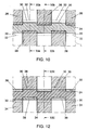
- FIG. 12 shows a top view of the wafer after the "lift-off" step.
- FIG. 13 shows a transverse section along the line XIII-XIII in FIG. 12 through a half-strip 34 after the second etching step.
- a cleaning step is again performed as the last step, in which the remaining quartz sections, viz. the strip 24 and the half-strips 34 and 36 of the first and the third mask pattern, respectively, are removed.
- the first mask pattern instead of an elongated strip having constant width over its entire length, an elongated strip having alternately wide and narrow part strips or, alternatively, a strip having identical part strips which are joined to one another in an offset manner.
- a similar alignment of the second mask pattern with respect to the first mask pattern is necessary, as indicated in the embodiment described with reference to FIG. 4 to FIG. 9 inclusive.
Landscapes
- Physics & Mathematics (AREA)
- General Physics & Mathematics (AREA)
- Optics & Photonics (AREA)
- Engineering & Computer Science (AREA)
- Microelectronics & Electronic Packaging (AREA)
- Optical Integrated Circuits (AREA)
- Optical Couplings Of Light Guides (AREA)
Claims (12)
- Polarisationswandler zur Wandlung eines Anteiles einer Signalkomponente, die sich gemäss einem ersten geführten Mode ausbreitet, eines optischen Signals in eine Signalkomponente, die sich gemäss einem zweiten geführten Mode ausbreitet, wobei die ersten und zweiten Moden jeweils verschiedene Polarisationsmoden betreffen, mit einem Kanalwellenleiter, der von einem Substrat (S) getragen wird, wobei in diesem Wellenleiter eine periodische Kopplung zwischen den besagten geführten Moden des optischen Signals stattfindet, welches sich in dem Wellenleiter ausbreitet, wobei der Wellenleiter einen eintretenden Wellenleiterabschnitt (A), einen mittleren Wellenleiterabschnitt (B) und einen austretenden Wellenleiterabschnitt (C) aufweist, wobei der mittlere Wellenleiterabschnitt eine periodische geometrische Struktur aufweist, die eine periodische Verkettung von zwei wellenleitenden Unterabschnitten (P, Q) innerhalb einer Periodenlänge aufweist, die mit verschiedenen Wellenleiterprofilen ausgestattet sind, die im wesentlichen durch Streifenelemente (S3, S4) bestimmt werden, dadurch gekennzeichnet, dass die Streifenelemente (S3, S4 ; 12, 22) mit Seitenwänden versehen sind, die in bezug auf die Substratebene in Winkeln geneigt sind, die gegenüber dem oder denen des oder der benachbarten Streifenelemente unterschiedlich sind.
- Polarisationswandler nach Anspruch 1, dadurch gekennzeichnet, dass die Streifenelemente von den zwei Unterabschnitten in Richtung quer zu ihrer longitudinalen Ausrichtung zueinander unterschiedliche trapezförmige Querschnitte aufweisen.
- Polarisationswandler nach Anspruch 2, dadurch gekennzeichnet, dass die Querschnitte der Streifenelemente von einem ersten und dem zweiten der beiden Unterabschnitte im wesentlichen ein Rechteck (Δ1 = Δ2 = 0 in Fig. 3) und ein gleichseitiges Trapez (Δ1 = Δ2 ≠ 0) sind.
- Polarisationswandler nach Anspruch 2, dadurch gekennzeichnet, dass die Querschnitte der Streifenelemente der beiden Unterabschnitte im wesentlichen rechtwinklige Trapeze sind, wobei eines ein links-rechtwinkliges Trapez (Δ1 = 0, Δ2 ≠ 0 in Fig. 3) und das andere ein rechts-rechtwinkliges Trapez (Δ1 ≠ 0, Δ2 = 0 in Fig. 3) ist.
- Polarisationswandler nach Anspruch 2, 3 oder 4, dadurch gekennzeichnet, dass die Querschnitte im wesentlichen die gleiche Höhe (h) aufweisen.
- Verfahren zur Herstellung eines Kanalwellenleiterabschnittes (B) für einen Polarisationswandler nach Anspruch 2 auf einer Substratschicht (8) aus kristallinem Material und die mit einer lichtleitenden Schicht (S2, 10) versehen ist, wobei der Kanalwellenleiterabschnitt eine periodische Verkettung von zwei Wellenleiterunterabschnitten (P, Q) je Periode aufweist, und wobei die zwei Wellenleiterunterabschnitte durch Streifenelemente (S3,S4) definiert werden, die vertikale und geneigte Seitenwände aufweisen, dadurch gekennzeichnet, dass das Verfahren die folgenden Schritte umfasst:wobei die ersten und zweiten Maskenmuster so dimensioniert sind, um die Streifenelemente zur periodischen Verkettung der Wellenleiterunterabschnitte zu definieren, unda) Auftragen einer Schichtstruktur (L), welche das Substrat (8) und die lichtleitende Schicht (10), ein erstes Streifenmaskenmuster (2) eines ersten Maskenmaterials in einer vorbestimmten Richtung relativ zur Kristallorientation der lichtleitenden Schicht umfasst,b) Auftragen auf die Schichtstruktur (L) und teilweise über das erste Maskenmuster eines zweiten Maskenmusters eines zweiten Maskenmaterials, wobei das zweite Maskenmaterial eine Anzahl von parallelen Streifenuntermustern (14; 26, 28) aufweist, die im wesentlichen quer zu und zumindest teilweise über dem ersten Streifenmaskenmuster liegen,c) einen ersten Ätzschritt unter Einsatz von ersten Ätzmitteln auf Teilen der Schichtstruktur, die nicht von den ersten und zweiten Maskenmaterialien abgedeckt sind,d) Entfernen des zweiten Maskenmaterials,e) Abdecken der im ersten Ätzschritt geätzten Teile mit einem dritten Maskenmaterial (20; 34, 36),f) einen zweiten Ätzschritt unter Einsatz von zweiten Ätzmitteln von Teilen der Schichtstruktur, die nicht von den ersten und dritten Maskenmaterialien abgedeckt sind, undg) Entfernen der ersten und dritten Maskenmaterialien,
dass einer der zwei Atzschritte ein Nassätzschritt ist, der mit Nassätzmitteln durchgeführt wird, um geneigte Seitenwände der Streifenelemente gemäss der vorbestimmten Richtung des ersten Maskenmusters zu erzeugen, und dass der andere Ätzschritt ein Trockenätzschritt ist, der mit Trockenätzmitteln durchgeführt wird, um vertikale Seitenwände der Streifenelemente zu ätzen. - Verfahren nach Anspruch 6, dadurch gekennzeichnet, dass der Schritt (c) mit Nassätzmitteln durchgeführt wird und dass die Schritte (d) und (e) mit einer Abhebetechnik durchgeführt werden, welche die folgenden Unterschritte umfasst:(de1) - Abdecken des ersten und zweiten Maskenmusters und der geätzten Abschnitte der Schichtstruktur mit einer Maskenschicht aus einem mit dem ersten Maskenmaterial identischen Maskenmaterial, und(de2) - Entfernen des zweiten Maskenmaterials mit einem geeigneten Lösungsmittel, inklusive den Anteilen des ersten Maskenmaterials, die auf ihm angeordnet sind.
- Verfahren nach Anspruch 6 oder 7, dadurch gekennzeichnet, dass das streifenförmige erste Maskenmuster in der longitudinalen Richtung wechselweise breite und dünne Teilstreifen aufweist, und dass das Streifenuntermuster des zweiten Maskenmusters entweder nur die breiten Teilstreifen oder nur die dünnen Teilstreifen des ersten Maskenmusters des ersten Maskenmusters vollständig abdeckt.
- Verfahren nach Anspruch 6 oder 7, dadurch gekennzeichnet, dass das streifenförmige erste Maskenmuster in der longitudinalen Richtung wechselweise breite und dünne Teilstreifen aufweist, und dass das Streifenuntermuster des zweiten Maskenmusters das erste Maskenmuster auf der selben Seite der breiten Teilstreifen und auf der gegenüberliegenden Seite der dünnen Teilstreifen teilweise abdeckt.
- Verfahren nach Anspruch 6 oder 7, dadurch gekennzeichnet, dass das streifenförmige erste Maskenmuster einen länglichen Streifen konstanter Breite in der longitudinalen Richtung umfasst.
- Verfahren nach Anspruch 6 oder 7, dadurch gekennzeichnet, dass das streifenförmige erste Maskenmuster in der longitudinalen Richtung Teilstreifen gleicher Breite aufweist, wobei diese Teilstreifen mit einem seitlichen Versatz wechselweise in der einen und in der anderen Richtung aneinander angesetzt sind, und dass das Streifenuntermuster des zweiten Maskenmusters das erste Maskenmuster mit einem Versatz in der einen Richtung auf der gleichen Seite der Teilstreifen und mit einem Versatz in der anderen Richtung auf der anderen gegenüberliegenden Seite der Teilstreifen teilweise abdeckt.
- Verfahren nach Anspruch 6, 7, 8, 9, 10 oder 11, dadurch gekennzeichnet, dass das zweite Maskenmaterial ein photosensitives Material ist.
Applications Claiming Priority (2)
| Application Number | Priority Date | Filing Date | Title |
|---|---|---|---|
| NL9301656 | 1993-09-24 | ||
| NL9301656A NL9301656A (nl) | 1993-09-24 | 1993-09-24 | Geintegreerde optische polarisatie-omzetter met versterkte periodieke koppeling. |
Publications (2)
| Publication Number | Publication Date |
|---|---|
| EP0645650A1 EP0645650A1 (de) | 1995-03-29 |
| EP0645650B1 true EP0645650B1 (de) | 1998-12-23 |
Family
ID=19862924
Family Applications (1)
| Application Number | Title | Priority Date | Filing Date |
|---|---|---|---|
| EP94202591A Expired - Lifetime EP0645650B1 (de) | 1993-09-24 | 1994-09-09 | Integrierter optischer Polarisationswandler mit erhöhter periodischer Kopplung |
Country Status (7)
| Country | Link |
|---|---|
| US (1) | US5539845A (de) |
| EP (1) | EP0645650B1 (de) |
| JP (1) | JP2934719B2 (de) |
| AT (1) | ATE175031T1 (de) |
| DE (1) | DE69415455T2 (de) |
| ES (1) | ES2127883T3 (de) |
| NL (1) | NL9301656A (de) |
Cited By (1)
| Publication number | Priority date | Publication date | Assignee | Title |
|---|---|---|---|---|
| US6973110B2 (en) | 2002-02-22 | 2005-12-06 | Infineon Technologies Ag | Monolithic laser configuration |
Families Citing this family (27)
| Publication number | Priority date | Publication date | Assignee | Title |
|---|---|---|---|---|
| TW347597B (en) * | 1994-01-31 | 1998-12-11 | Mitsubishi Chem Corp | Method of forming a groove in a semiconductor laser diode and a semiconductor laser diode |
| NL1000759C2 (nl) * | 1995-07-07 | 1997-01-08 | Nederland Ptt | Geïntegreerde optische modus-omzetter. |
| NL1001777C2 (nl) * | 1995-11-29 | 1997-05-30 | Nederland Ptt | Werkwijze voor het vervaardigen van scherpe golfgeleider-vertakkingen in geïntegreerde optische circuits. |
| US5799119A (en) * | 1996-07-03 | 1998-08-25 | Northern Telecom Limited | Coupling of strongly and weakly guiding waveguides for compact integrated mach zehnder modulators |
| US5796906A (en) * | 1996-08-27 | 1998-08-18 | Lucent Technologies Inc. | Optical planar waveguide notch filters |
| US5973833A (en) * | 1997-08-29 | 1999-10-26 | Lightware, Inc. | High efficiency polarizing converter |
| FR2781577B1 (fr) * | 1998-07-06 | 2000-09-08 | Alsthom Cge Alcatel | Procede de fabrication d'un circuit optique integre |
| US6809420B1 (en) * | 2000-02-29 | 2004-10-26 | Intel Corporation | Characterization of induced shift on an overlay target using post-etch artifact wafers |
| US6373630B1 (en) | 2000-05-05 | 2002-04-16 | Chih-Kung Lee | Light beam polarization converter |
| US6539150B2 (en) | 2000-12-13 | 2003-03-25 | Alcatel Optronics Uk Limited | Segmented waveguide flattening the passband of a phasar |
| GB2384319A (en) * | 2002-01-19 | 2003-07-23 | Marconi Optical Components Ltd | Polarisation converter for photonic crystal waveguide |
| DE10209063C1 (de) * | 2002-02-22 | 2003-10-30 | Infineon Technologies Ag | Verfahren zur Herstellung einer monolithischen Laseranordnung |
| US7218814B2 (en) | 2002-05-28 | 2007-05-15 | Optun (Bvi) Ltd. | Method and apparatus for optical mode conversion |
| US7321705B2 (en) | 2002-05-28 | 2008-01-22 | Optun (Bvi) Ltd. | Method and device for optical switching and variable optical attenuation |
| US7609918B2 (en) | 2002-05-28 | 2009-10-27 | Optun (Bvi) Ltd. | Method and apparatus for optical mode division multiplexing and demultiplexing |
| US20040096136A1 (en) * | 2002-11-18 | 2004-05-20 | Harmeet Singh | Integrated polarization rotator |
| EP1473576A1 (de) * | 2003-05-02 | 2004-11-03 | ThreeFive Photonics B.V. | Integrierte optische Wellenleiter |
| US7792403B1 (en) * | 2005-09-08 | 2010-09-07 | Infinera Corporation | Adiabatic polarization converter |
| DE102007004043A1 (de) * | 2007-01-22 | 2008-07-31 | Universität Karlsruhe (Th) | Herstellungsverfahren für halbleiterbasierte optische Wellenleiterstrukturen mit speziellen geometrischen Formen |
| US7565041B2 (en) * | 2007-10-26 | 2009-07-21 | Infinera Corporation | Symmetric optical circuit with integrated polarization rotator |
| CN101320113B (zh) * | 2008-07-15 | 2010-06-09 | 浙江大学 | 一种波导型偏振模式转换器 |
| CN104040394B (zh) * | 2011-12-05 | 2018-02-06 | 埃因霍温科技大学 | 增加的容差的偏振转换器 |
| US8854931B2 (en) * | 2013-03-08 | 2014-10-07 | Tdk Corporation | Polarization converter including a jagged diagonal line in plane orthogonal to propagation direction of electromagnetic wave |
| JP6264922B2 (ja) * | 2014-02-13 | 2018-01-24 | 沖電気工業株式会社 | 光波長フィルタ及び合分波素子 |
| JP6402519B2 (ja) * | 2014-07-18 | 2018-10-10 | 沖電気工業株式会社 | 光導波路素子 |
| JP6077076B1 (ja) * | 2015-09-11 | 2017-02-08 | 株式会社東芝 | グラフェン配線構造及びグラフェン配線構造の作製方法 |
| DE102016202634A1 (de) * | 2016-02-19 | 2017-08-24 | Fraunhofer-Gesellschaft zur Förderung der angewandten Forschung e.V. | Verfahren zum Herstellen eines Polarisationskonverters, Polarisationskonverter und Polarisationskonverterelement |
Family Cites Families (17)
| Publication number | Priority date | Publication date | Assignee | Title |
|---|---|---|---|---|
| US3614198A (en) * | 1969-06-23 | 1971-10-19 | Bell Telephone Labor Inc | Thin-film optical devices |
| US3884549A (en) * | 1973-04-30 | 1975-05-20 | Univ California | Two demensional distributed feedback devices and lasers |
| US4359260A (en) * | 1980-06-25 | 1982-11-16 | Bell Telephone Laboratories, Incorporated | Optical polarizer |
| JPS59171187A (ja) * | 1983-03-18 | 1984-09-27 | Hitachi Ltd | 半導体レ−ザ装置 |
| DE3341482A1 (de) * | 1983-11-17 | 1985-05-30 | Philips Patentverwaltung Gmbh, 2000 Hamburg | Magneto-optische wellenleiterstruktur mit kuenstlicher optischer anisotropie |
| FR2584826B1 (fr) * | 1985-07-11 | 1987-10-09 | Labo Electronique Physique | Element de commutation optique entre deux guides de lumiere et matrice de commutation optique formee de ces elements de commutation |
| FR2584825B1 (fr) * | 1985-07-11 | 1987-10-09 | Labo Electronique Physique | Structure separatrice, element de commutation optique incluant de telles structures et matrice de commutation optique formee de ces elements de commutation |
| GB2187566A (en) * | 1986-03-07 | 1987-09-09 | Philips Electronic Associated | Device for doubling the frequency of electromagnetic radiation |
| JPH01183184A (ja) * | 1988-01-18 | 1989-07-20 | Canon Inc | 半導体レーザーとその製造方法 |
| FR2634905B1 (fr) * | 1988-07-05 | 1990-10-05 | Labo Electronique Physique | Dispositif semiconducteur optoelectronique integre incluant un separateur des polarisations te/tm |
| JPH0422904A (ja) * | 1990-05-18 | 1992-01-27 | Omron Corp | リブ形光導波路 |
| US4974931A (en) * | 1989-11-13 | 1990-12-04 | At&T Bell Laboratories | Wavelength selective mode couplers |
| JPH03288104A (ja) * | 1990-04-04 | 1991-12-18 | Agency Of Ind Science & Technol | 一方向性モード変換器およびそれを用いた光アイソレータ |
| US5078516A (en) * | 1990-11-06 | 1992-01-07 | Bell Communications Research, Inc. | Tapered rib waveguides |
| NL9100852A (nl) * | 1991-05-16 | 1992-12-16 | Nederland Ptt | Modusomzetter. |
| SE509264C2 (sv) * | 1992-01-30 | 1998-12-21 | Ericsson Telefon Ab L M | Anordning och förfarande för polarisationsoberoende behandling av en optisk signal i en vågledare |
| FR2850661A1 (fr) * | 2003-02-04 | 2004-08-06 | Atofina | Procede de preparation d'un materiau composite comprenant un polymere et des nanoparticules metalliques |
-
1993
- 1993-09-24 NL NL9301656A patent/NL9301656A/nl not_active Application Discontinuation
-
1994
- 1994-09-09 ES ES94202591T patent/ES2127883T3/es not_active Expired - Lifetime
- 1994-09-09 AT AT94202591T patent/ATE175031T1/de not_active IP Right Cessation
- 1994-09-09 DE DE69415455T patent/DE69415455T2/de not_active Expired - Lifetime
- 1994-09-09 EP EP94202591A patent/EP0645650B1/de not_active Expired - Lifetime
- 1994-09-26 JP JP6265973A patent/JP2934719B2/ja not_active Expired - Lifetime
-
1995
- 1995-06-07 US US08/485,653 patent/US5539845A/en not_active Expired - Lifetime
Cited By (1)
| Publication number | Priority date | Publication date | Assignee | Title |
|---|---|---|---|---|
| US6973110B2 (en) | 2002-02-22 | 2005-12-06 | Infineon Technologies Ag | Monolithic laser configuration |
Also Published As
| Publication number | Publication date |
|---|---|
| JPH07168045A (ja) | 1995-07-04 |
| DE69415455D1 (de) | 1999-02-04 |
| ES2127883T3 (es) | 1999-05-01 |
| US5539845A (en) | 1996-07-23 |
| NL9301656A (nl) | 1995-04-18 |
| EP0645650A1 (de) | 1995-03-29 |
| JP2934719B2 (ja) | 1999-08-16 |
| ATE175031T1 (de) | 1999-01-15 |
| DE69415455T2 (de) | 1999-06-10 |
Similar Documents
| Publication | Publication Date | Title |
|---|---|---|
| EP0645650B1 (de) | Integrierter optischer Polarisationswandler mit erhöhter periodischer Kopplung | |
| EP0228886B1 (de) | Optischer Wellenleiter mit einer Schichtstruktur | |
| US7239779B2 (en) | Broadband optical via | |
| EP0632300B1 (de) | Optische Wellenlängenmultiplex- und -demultiplexvorrichtung zum Multiplexen oder Demultiplexen von Licht mit mehreren Moden und damit versehener Photodetektor | |
| US6853791B2 (en) | Waveguide bends and splitters in slab photonic crystals with noncircular holes | |
| US20040264903A1 (en) | Intergrated photonic crystal structure and method of producing same | |
| US8494314B2 (en) | Fabrication tolerant polarization converter | |
| Korotky et al. | Greatly reduced losses for small‐radius bends in Ti: LiNbO3 waveguides | |
| JPH07253515A (ja) | 光学導波路の変換器とその製造方法 | |
| JP3028288B2 (ja) | 集積型光モード変換器とその製造方法 | |
| EP3316011A1 (de) | Vorrichtung und verfahren für einen verlustarmen resonator mit hohem q-faktor | |
| US6097865A (en) | Design and method for planar coupled waveguide filter | |
| Hayes et al. | GaAs spiral optical waveguides for delay-line applications | |
| US20240353618A1 (en) | Light polarisation converter and method of manufacture | |
| Leonberger et al. | Low‐loss GaAs optical waveguides formed by lateral epitaxial growth over oxide | |
| Groen et al. | Compact polarisation converter on InP/InGaAsP using an asymmetrical waveguide | |
| KR930010131B1 (ko) | 테이퍼형 반도체 도파관 및 그의 제조방법 | |
| CN118057224A (zh) | 具有相邻的超材料结构的光学组件 | |
| JP3112115B2 (ja) | 光導波路の製造方法 | |
| JP3409605B2 (ja) | 半導体偏波回転素子 | |
| WO2004008203A1 (en) | Planar waveguide with tapered region | |
| US20250355288A1 (en) | Optical devices having improved mode transitions | |
| JP3409606B2 (ja) | 半導体偏波回転素子 | |
| Leick et al. | Achieving small process tolerant wavelength-flattened 3 dB directional couplers in silica-on-silicon | |
| US7680383B1 (en) | Semiconductor-based broadband modulators |
Legal Events
| Date | Code | Title | Description |
|---|---|---|---|
| PUAI | Public reference made under article 153(3) epc to a published international application that has entered the european phase |
Free format text: ORIGINAL CODE: 0009012 |
|
| AK | Designated contracting states |
Kind code of ref document: A1 Designated state(s): AT BE CH DE DK ES FR GB GR IE IT LI LU NL PT SE |
|
| 17P | Request for examination filed |
Effective date: 19950907 |
|
| 17Q | First examination report despatched |
Effective date: 19970825 |
|
| GRAG | Despatch of communication of intention to grant |
Free format text: ORIGINAL CODE: EPIDOS AGRA |
|
| GRAG | Despatch of communication of intention to grant |
Free format text: ORIGINAL CODE: EPIDOS AGRA |
|
| GRAH | Despatch of communication of intention to grant a patent |
Free format text: ORIGINAL CODE: EPIDOS IGRA |
|
| GRAH | Despatch of communication of intention to grant a patent |
Free format text: ORIGINAL CODE: EPIDOS IGRA |
|
| GRAA | (expected) grant |
Free format text: ORIGINAL CODE: 0009210 |
|
| RAP3 | Party data changed (applicant data changed or rights of an application transferred) |
Owner name: KONINKLIJKE KPN N.V. |
|
| AK | Designated contracting states |
Kind code of ref document: B1 Designated state(s): AT BE CH DE DK ES FR GB GR IE IT LI LU NL PT SE |
|
| PG25 | Lapsed in a contracting state [announced via postgrant information from national office to epo] |
Ref country code: GR Free format text: LAPSE BECAUSE OF NON-PAYMENT OF DUE FEES Effective date: 19981223 |
|
| REF | Corresponds to: |
Ref document number: 175031 Country of ref document: AT Date of ref document: 19990115 Kind code of ref document: T |
|
| REG | Reference to a national code |
Ref country code: CH Ref legal event code: NV Representative=s name: ISLER & PEDRAZZINI AG Ref country code: CH Ref legal event code: EP |
|
| REF | Corresponds to: |
Ref document number: 69415455 Country of ref document: DE Date of ref document: 19990204 |
|
| REG | Reference to a national code |
Ref country code: IE Ref legal event code: FG4D |
|
| ITF | It: translation for a ep patent filed | ||
| PG25 | Lapsed in a contracting state [announced via postgrant information from national office to epo] |
Ref country code: PT Free format text: LAPSE BECAUSE OF FAILURE TO SUBMIT A TRANSLATION OF THE DESCRIPTION OR TO PAY THE FEE WITHIN THE PRESCRIBED TIME-LIMIT Effective date: 19990323 Ref country code: DK Free format text: LAPSE BECAUSE OF FAILURE TO SUBMIT A TRANSLATION OF THE DESCRIPTION OR TO PAY THE FEE WITHIN THE PRESCRIBED TIME-LIMIT Effective date: 19990323 |
|
| ET | Fr: translation filed | ||
| REG | Reference to a national code |
Ref country code: ES Ref legal event code: FG2A Ref document number: 2127883 Country of ref document: ES Kind code of ref document: T3 |
|
| PLBE | No opposition filed within time limit |
Free format text: ORIGINAL CODE: 0009261 |
|
| STAA | Information on the status of an ep patent application or granted ep patent |
Free format text: STATUS: NO OPPOSITION FILED WITHIN TIME LIMIT |
|
| 26N | No opposition filed | ||
| REG | Reference to a national code |
Ref country code: GB Ref legal event code: IF02 |
|
| PGFP | Annual fee paid to national office [announced via postgrant information from national office to epo] |
Ref country code: CH Payment date: 20040909 Year of fee payment: 11 |
|
| PGFP | Annual fee paid to national office [announced via postgrant information from national office to epo] |
Ref country code: LU Payment date: 20040910 Year of fee payment: 11 Ref country code: AT Payment date: 20040910 Year of fee payment: 11 |
|
| PG25 | Lapsed in a contracting state [announced via postgrant information from national office to epo] |
Ref country code: AT Free format text: LAPSE BECAUSE OF NON-PAYMENT OF DUE FEES Effective date: 20050909 |
|
| PG25 | Lapsed in a contracting state [announced via postgrant information from national office to epo] |
Ref country code: LU Free format text: LAPSE BECAUSE OF NON-PAYMENT OF DUE FEES Effective date: 20050930 Ref country code: LI Free format text: LAPSE BECAUSE OF NON-PAYMENT OF DUE FEES Effective date: 20050930 Ref country code: CH Free format text: LAPSE BECAUSE OF NON-PAYMENT OF DUE FEES Effective date: 20050930 |
|
| REG | Reference to a national code |
Ref country code: CH Ref legal event code: PL |
|
| PGFP | Annual fee paid to national office [announced via postgrant information from national office to epo] |
Ref country code: IE Payment date: 20090921 Year of fee payment: 16 Ref country code: ES Payment date: 20090922 Year of fee payment: 16 |
|
| PGFP | Annual fee paid to national office [announced via postgrant information from national office to epo] |
Ref country code: SE Payment date: 20090915 Year of fee payment: 16 Ref country code: NL Payment date: 20090915 Year of fee payment: 16 |
|
| PGFP | Annual fee paid to national office [announced via postgrant information from national office to epo] |
Ref country code: IT Payment date: 20090926 Year of fee payment: 16 |
|
| PGFP | Annual fee paid to national office [announced via postgrant information from national office to epo] |
Ref country code: BE Payment date: 20091023 Year of fee payment: 16 |
|
| REG | Reference to a national code |
Ref country code: FR Ref legal event code: TP |
|
| REG | Reference to a national code |
Ref country code: GB Ref legal event code: 732E Free format text: REGISTERED BETWEEN 20100617 AND 20100623 |
|
| REG | Reference to a national code |
Ref country code: NL Ref legal event code: SD Effective date: 20100720 |
|
| PGFP | Annual fee paid to national office [announced via postgrant information from national office to epo] |
Ref country code: DE Payment date: 20100930 Year of fee payment: 17 |
|
| BERE | Be: lapsed |
Owner name: AMSTR. INVESTMENTS 23 K.G. LLC Effective date: 20100930 |
|
| REG | Reference to a national code |
Ref country code: NL Ref legal event code: V1 Effective date: 20110401 |
|
| REG | Reference to a national code |
Ref country code: SE Ref legal event code: EUG |
|
| PG25 | Lapsed in a contracting state [announced via postgrant information from national office to epo] |
Ref country code: IT Free format text: LAPSE BECAUSE OF NON-PAYMENT OF DUE FEES Effective date: 20100909 |
|
| REG | Reference to a national code |
Ref country code: IE Ref legal event code: MM4A |
|
| PG25 | Lapsed in a contracting state [announced via postgrant information from national office to epo] |
Ref country code: IE Free format text: LAPSE BECAUSE OF NON-PAYMENT OF DUE FEES Effective date: 20100909 Ref country code: BE Free format text: LAPSE BECAUSE OF NON-PAYMENT OF DUE FEES Effective date: 20100930 |
|
| PG25 | Lapsed in a contracting state [announced via postgrant information from national office to epo] |
Ref country code: NL Free format text: LAPSE BECAUSE OF NON-PAYMENT OF DUE FEES Effective date: 20110401 |
|
| REG | Reference to a national code |
Ref country code: ES Ref legal event code: FD2A Effective date: 20111019 |
|
| PG25 | Lapsed in a contracting state [announced via postgrant information from national office to epo] |
Ref country code: ES Free format text: LAPSE BECAUSE OF NON-PAYMENT OF DUE FEES Effective date: 20100910 |
|
| PG25 | Lapsed in a contracting state [announced via postgrant information from national office to epo] |
Ref country code: SE Free format text: LAPSE BECAUSE OF NON-PAYMENT OF DUE FEES Effective date: 20100910 |
|
| PGFP | Annual fee paid to national office [announced via postgrant information from national office to epo] |
Ref country code: GB Payment date: 20120829 Year of fee payment: 19 |
|
| PGFP | Annual fee paid to national office [announced via postgrant information from national office to epo] |
Ref country code: FR Payment date: 20120910 Year of fee payment: 19 |
|
| PG25 | Lapsed in a contracting state [announced via postgrant information from national office to epo] |
Ref country code: DE Free format text: LAPSE BECAUSE OF NON-PAYMENT OF DUE FEES Effective date: 20130403 |
|
| REG | Reference to a national code |
Ref country code: DE Ref legal event code: R119 Ref document number: 69415455 Country of ref document: DE Effective date: 20130403 |
|
| GBPC | Gb: european patent ceased through non-payment of renewal fee |
Effective date: 20130909 |
|
| REG | Reference to a national code |
Ref country code: FR Ref legal event code: ST Effective date: 20140530 |
|
| PG25 | Lapsed in a contracting state [announced via postgrant information from national office to epo] |
Ref country code: GB Free format text: LAPSE BECAUSE OF NON-PAYMENT OF DUE FEES Effective date: 20130909 |
|
| PG25 | Lapsed in a contracting state [announced via postgrant information from national office to epo] |
Ref country code: FR Free format text: LAPSE BECAUSE OF NON-PAYMENT OF DUE FEES Effective date: 20130930 |