EP0638424A2 - Tête d'impression par jet d'encre thermique et méthode de fabrication - Google Patents
Tête d'impression par jet d'encre thermique et méthode de fabrication Download PDFInfo
- Publication number
- EP0638424A2 EP0638424A2 EP94305204A EP94305204A EP0638424A2 EP 0638424 A2 EP0638424 A2 EP 0638424A2 EP 94305204 A EP94305204 A EP 94305204A EP 94305204 A EP94305204 A EP 94305204A EP 0638424 A2 EP0638424 A2 EP 0638424A2
- Authority
- EP
- European Patent Office
- Prior art keywords
- heater resistor
- substrate
- heater
- feed opening
- ink feed
- Prior art date
- Legal status (The legal status is an assumption and is not a legal conclusion. Google has not performed a legal analysis and makes no representation as to the accuracy of the status listed.)
- Withdrawn
Links
- 238000000034 method Methods 0.000 title claims abstract description 33
- 238000004519 manufacturing process Methods 0.000 title abstract description 6
- 239000000758 substrate Substances 0.000 claims abstract description 34
- 230000004888 barrier function Effects 0.000 claims abstract description 20
- 238000010304 firing Methods 0.000 claims abstract description 19
- 239000010409 thin film Substances 0.000 claims abstract description 19
- 230000008569 process Effects 0.000 claims description 21
- 239000000463 material Substances 0.000 claims description 10
- 239000004020 conductor Substances 0.000 claims description 5
- 238000007641 inkjet printing Methods 0.000 claims description 3
- 238000000151 deposition Methods 0.000 claims description 2
- 239000010410 layer Substances 0.000 description 24
- 229910052782 aluminium Inorganic materials 0.000 description 17
- XAGFODPZIPBFFR-UHFFFAOYSA-N aluminium Chemical compound [Al] XAGFODPZIPBFFR-UHFFFAOYSA-N 0.000 description 17
- RVSGESPTHDDNTH-UHFFFAOYSA-N alumane;tantalum Chemical compound [AlH3].[Ta] RVSGESPTHDDNTH-UHFFFAOYSA-N 0.000 description 9
- VYPSYNLAJGMNEJ-UHFFFAOYSA-N Silicium dioxide Chemical compound O=[Si]=O VYPSYNLAJGMNEJ-UHFFFAOYSA-N 0.000 description 8
- 229920000642 polymer Polymers 0.000 description 8
- 238000005530 etching Methods 0.000 description 7
- 230000000873 masking effect Effects 0.000 description 7
- 229910052581 Si3N4 Inorganic materials 0.000 description 6
- HBMJWWWQQXIZIP-UHFFFAOYSA-N silicon carbide Chemical compound [Si+]#[C-] HBMJWWWQQXIZIP-UHFFFAOYSA-N 0.000 description 6
- 229910010271 silicon carbide Inorganic materials 0.000 description 6
- XUIMIQQOPSSXEZ-UHFFFAOYSA-N Silicon Chemical compound [Si] XUIMIQQOPSSXEZ-UHFFFAOYSA-N 0.000 description 5
- 238000010276 construction Methods 0.000 description 5
- 238000005553 drilling Methods 0.000 description 5
- 229910052710 silicon Inorganic materials 0.000 description 5
- 239000010703 silicon Substances 0.000 description 5
- 238000012856 packing Methods 0.000 description 4
- 229920002120 photoresistant polymer Polymers 0.000 description 4
- 235000012239 silicon dioxide Nutrition 0.000 description 4
- 239000000377 silicon dioxide Substances 0.000 description 4
- 230000008901 benefit Effects 0.000 description 3
- 230000006872 improvement Effects 0.000 description 3
- 238000002161 passivation Methods 0.000 description 3
- 230000009467 reduction Effects 0.000 description 3
- 238000003486 chemical etching Methods 0.000 description 2
- 229910052681 coesite Inorganic materials 0.000 description 2
- 229910052906 cristobalite Inorganic materials 0.000 description 2
- 238000002955 isolation Methods 0.000 description 2
- 238000012986 modification Methods 0.000 description 2
- 230000004048 modification Effects 0.000 description 2
- 229910003465 moissanite Inorganic materials 0.000 description 2
- 238000000623 plasma-assisted chemical vapour deposition Methods 0.000 description 2
- 229910021420 polycrystalline silicon Inorganic materials 0.000 description 2
- 238000005488 sandblasting Methods 0.000 description 2
- HQVNEWCFYHHQES-UHFFFAOYSA-N silicon nitride Chemical compound N12[Si]34N5[Si]62N3[Si]51N64 HQVNEWCFYHHQES-UHFFFAOYSA-N 0.000 description 2
- 238000004544 sputter deposition Methods 0.000 description 2
- 229910052682 stishovite Inorganic materials 0.000 description 2
- 239000002344 surface layer Substances 0.000 description 2
- 229910052905 tridymite Inorganic materials 0.000 description 2
- 230000015572 biosynthetic process Effects 0.000 description 1
- 230000008859 change Effects 0.000 description 1
- 239000002131 composite material Substances 0.000 description 1
- 238000005516 engineering process Methods 0.000 description 1
- 230000002708 enhancing effect Effects 0.000 description 1
- 238000010438 heat treatment Methods 0.000 description 1
- 239000012535 impurity Substances 0.000 description 1
- 229910052751 metal Inorganic materials 0.000 description 1
- 239000002184 metal Substances 0.000 description 1
- 150000002739 metals Chemical class 0.000 description 1
- 229920005591 polysilicon Polymers 0.000 description 1
- 230000001681 protective effect Effects 0.000 description 1
- 239000002904 solvent Substances 0.000 description 1
- 238000000427 thin-film deposition Methods 0.000 description 1
- WFKWXMTUELFFGS-UHFFFAOYSA-N tungsten Chemical compound [W] WFKWXMTUELFFGS-UHFFFAOYSA-N 0.000 description 1
- 229910052721 tungsten Inorganic materials 0.000 description 1
- 239000010937 tungsten Substances 0.000 description 1
- 238000007740 vapor deposition Methods 0.000 description 1
Images


Classifications
-
- B—PERFORMING OPERATIONS; TRANSPORTING
- B41—PRINTING; LINING MACHINES; TYPEWRITERS; STAMPS
- B41J—TYPEWRITERS; SELECTIVE PRINTING MECHANISMS, i.e. MECHANISMS PRINTING OTHERWISE THAN FROM A FORME; CORRECTION OF TYPOGRAPHICAL ERRORS
- B41J2/00—Typewriters or selective printing mechanisms characterised by the printing or marking process for which they are designed
- B41J2/005—Typewriters or selective printing mechanisms characterised by the printing or marking process for which they are designed characterised by bringing liquid or particles selectively into contact with a printing material
- B41J2/01—Ink jet
- B41J2/135—Nozzles
- B41J2/16—Production of nozzles
- B41J2/1621—Manufacturing processes
- B41J2/1631—Manufacturing processes photolithography
-
- B—PERFORMING OPERATIONS; TRANSPORTING
- B41—PRINTING; LINING MACHINES; TYPEWRITERS; STAMPS
- B41J—TYPEWRITERS; SELECTIVE PRINTING MECHANISMS, i.e. MECHANISMS PRINTING OTHERWISE THAN FROM A FORME; CORRECTION OF TYPOGRAPHICAL ERRORS
- B41J2/00—Typewriters or selective printing mechanisms characterised by the printing or marking process for which they are designed
- B41J2/005—Typewriters or selective printing mechanisms characterised by the printing or marking process for which they are designed characterised by bringing liquid or particles selectively into contact with a printing material
- B41J2/01—Ink jet
- B41J2/135—Nozzles
- B41J2/14—Structure thereof only for on-demand ink jet heads
- B41J2/14016—Structure of bubble jet print heads
- B41J2/14088—Structure of heating means
- B41J2/14112—Resistive element
- B41J2/1412—Shape
-
- B—PERFORMING OPERATIONS; TRANSPORTING
- B41—PRINTING; LINING MACHINES; TYPEWRITERS; STAMPS
- B41J—TYPEWRITERS; SELECTIVE PRINTING MECHANISMS, i.e. MECHANISMS PRINTING OTHERWISE THAN FROM A FORME; CORRECTION OF TYPOGRAPHICAL ERRORS
- B41J2/00—Typewriters or selective printing mechanisms characterised by the printing or marking process for which they are designed
- B41J2/005—Typewriters or selective printing mechanisms characterised by the printing or marking process for which they are designed characterised by bringing liquid or particles selectively into contact with a printing material
- B41J2/01—Ink jet
- B41J2/135—Nozzles
- B41J2/14—Structure thereof only for on-demand ink jet heads
- B41J2/14016—Structure of bubble jet print heads
- B41J2/14088—Structure of heating means
- B41J2/14112—Resistive element
- B41J2/14129—Layer structure
-
- B—PERFORMING OPERATIONS; TRANSPORTING
- B41—PRINTING; LINING MACHINES; TYPEWRITERS; STAMPS
- B41J—TYPEWRITERS; SELECTIVE PRINTING MECHANISMS, i.e. MECHANISMS PRINTING OTHERWISE THAN FROM A FORME; CORRECTION OF TYPOGRAPHICAL ERRORS
- B41J2/00—Typewriters or selective printing mechanisms characterised by the printing or marking process for which they are designed
- B41J2/005—Typewriters or selective printing mechanisms characterised by the printing or marking process for which they are designed characterised by bringing liquid or particles selectively into contact with a printing material
- B41J2/01—Ink jet
- B41J2/135—Nozzles
- B41J2/16—Production of nozzles
- B41J2/1601—Production of bubble jet print heads
-
- B—PERFORMING OPERATIONS; TRANSPORTING
- B41—PRINTING; LINING MACHINES; TYPEWRITERS; STAMPS
- B41J—TYPEWRITERS; SELECTIVE PRINTING MECHANISMS, i.e. MECHANISMS PRINTING OTHERWISE THAN FROM A FORME; CORRECTION OF TYPOGRAPHICAL ERRORS
- B41J2/00—Typewriters or selective printing mechanisms characterised by the printing or marking process for which they are designed
- B41J2/005—Typewriters or selective printing mechanisms characterised by the printing or marking process for which they are designed characterised by bringing liquid or particles selectively into contact with a printing material
- B41J2/01—Ink jet
- B41J2/135—Nozzles
- B41J2/16—Production of nozzles
- B41J2/1621—Manufacturing processes
- B41J2/1626—Manufacturing processes etching
- B41J2/1629—Manufacturing processes etching wet etching
-
- B—PERFORMING OPERATIONS; TRANSPORTING
- B41—PRINTING; LINING MACHINES; TYPEWRITERS; STAMPS
- B41J—TYPEWRITERS; SELECTIVE PRINTING MECHANISMS, i.e. MECHANISMS PRINTING OTHERWISE THAN FROM A FORME; CORRECTION OF TYPOGRAPHICAL ERRORS
- B41J2/00—Typewriters or selective printing mechanisms characterised by the printing or marking process for which they are designed
- B41J2/005—Typewriters or selective printing mechanisms characterised by the printing or marking process for which they are designed characterised by bringing liquid or particles selectively into contact with a printing material
- B41J2/01—Ink jet
- B41J2/135—Nozzles
- B41J2/16—Production of nozzles
- B41J2/1621—Manufacturing processes
- B41J2/1632—Manufacturing processes machining
- B41J2/1634—Manufacturing processes machining laser machining
-
- B—PERFORMING OPERATIONS; TRANSPORTING
- B41—PRINTING; LINING MACHINES; TYPEWRITERS; STAMPS
- B41J—TYPEWRITERS; SELECTIVE PRINTING MECHANISMS, i.e. MECHANISMS PRINTING OTHERWISE THAN FROM A FORME; CORRECTION OF TYPOGRAPHICAL ERRORS
- B41J2/00—Typewriters or selective printing mechanisms characterised by the printing or marking process for which they are designed
- B41J2/005—Typewriters or selective printing mechanisms characterised by the printing or marking process for which they are designed characterised by bringing liquid or particles selectively into contact with a printing material
- B41J2/01—Ink jet
- B41J2/135—Nozzles
- B41J2/16—Production of nozzles
- B41J2/1621—Manufacturing processes
- B41J2/164—Manufacturing processes thin film formation
- B41J2/1642—Manufacturing processes thin film formation thin film formation by CVD [chemical vapor deposition]
-
- B—PERFORMING OPERATIONS; TRANSPORTING
- B41—PRINTING; LINING MACHINES; TYPEWRITERS; STAMPS
- B41J—TYPEWRITERS; SELECTIVE PRINTING MECHANISMS, i.e. MECHANISMS PRINTING OTHERWISE THAN FROM A FORME; CORRECTION OF TYPOGRAPHICAL ERRORS
- B41J2/00—Typewriters or selective printing mechanisms characterised by the printing or marking process for which they are designed
- B41J2/005—Typewriters or selective printing mechanisms characterised by the printing or marking process for which they are designed characterised by bringing liquid or particles selectively into contact with a printing material
- B41J2/01—Ink jet
- B41J2/135—Nozzles
- B41J2/16—Production of nozzles
- B41J2/1621—Manufacturing processes
- B41J2/164—Manufacturing processes thin film formation
- B41J2/1646—Manufacturing processes thin film formation thin film formation by sputtering
-
- B—PERFORMING OPERATIONS; TRANSPORTING
- B41—PRINTING; LINING MACHINES; TYPEWRITERS; STAMPS
- B41J—TYPEWRITERS; SELECTIVE PRINTING MECHANISMS, i.e. MECHANISMS PRINTING OTHERWISE THAN FROM A FORME; CORRECTION OF TYPOGRAPHICAL ERRORS
- B41J2202/00—Embodiments of or processes related to ink-jet or thermal heads
- B41J2202/01—Embodiments of or processes related to ink-jet heads
- B41J2202/11—Embodiments of or processes related to ink-jet heads characterised by specific geometrical characteristics
Definitions
- This invention relates generally to thermal ink jet (TIJ) pens useful in high speed computer driven ink jet printers and more particularly to such TIJ pens having improved ink feed and ink ejection characteristics and an improved heater resistor geometry and construction.
- TIJ thermal ink jet
- the invention disclosed and claimed in my above identified United States patent represents significant advances in the X-Y multiplex circuity for driving the TIJ pen, significant advances in increasing the printhead packing density on a thin film substrate, and also a significant improvement in the reduction of cross talk and improved cross talk isolation between adjacent heater resistors formed on a common thin film resistor printhead substrate.
- the general purpose and principal object of the present invention is to provide still further new and useful improvements with respect to my above identified patented invention and improvements which are particularly directed to enhancing the ink ejection efficiency and life of the thermal ink jet pen, while simultaneously maintaining a high level of cross talk reduction between adjacent heater resistors formed on a common thin film printhead substrate.
- Another object of this invention is to provide a new and improved thermal ink jet pen and method of manufacture of the type described which features improved ink ejection directionality as a result of the axial symmetry used in pen construction.
- the presence of a symmetric firing chamber in the novel printhead structure disclosed and claimed herein is operative to create ink drops fired normal to the pen surface.
- This structure is to be contrasted with current and prior art systems which are asymmetric in geometry and make ink drop directionality difficult to control.
- Another object of this invention is to provide a new and improved thermal ink pen of the type described which exhibits substantially improved ink ejection efficiency.
- the combined arrangement of the ink heater resistor, the ink fill channel, the ink firing chamber and the nozzle plate are all operative together in a novel structural combination to improve this ink ejection efficiency. Using this construction, there will be very little blow back down the ink feed channel, since the ink bubble growth is directed toward the nozzle plate in a symmetrical fashion.
- Another object of this invention is to provide a new and improved thermal ink jet pen of the type described which exhibits significantly improved refill rates due to the use of individual ink feed channels in combination with individual orifice or nozzle plate openings (orifii). This feature in turn reduces ink channel restrictions which are currently required in prior art pens to eliminate cross talk therein.
- Another object of this invention is to provide a new and improved thermal ink jet pen of the type described which is characterized by a significantly improved refill rate as a result of the reduction in the blow back down the ink feed hole of the TIJ pen.
- a heater resistor is formed to partially surround an ink feed passage located in a thin film printhead substrate.
- a barrier layer is disposed on the surface of the substrate and has an opening therein defining an ink firing chamber.
- An orifice plate is disposed on the barrier layer and has an orifice opening therein axially aligned with the central axis of the firing chamber an also with the central axis of the ink feed passage.
- Conductive trace lines are also disposed on the thin film resistor substrate and extend into electrical contact with the heater resistors to conduct electrical pulses to the heater resistors during a thermal ink jet printing operation.
- this process includes the steps of providing a thin film substrate and then forming a heater resistor region partially surrounding an area of the substrate in which an ink feed hole is to be subsequently formed.
- conductive trace lines are photolithographically defined on the surface of the substrate and extend into electrical contact with the heater resistor region.
- a polymer barrier layer material is deposited on the surface of the thin film substrate and is also photolithographically defined to create an opening in the barrier layer material. This opening surrounds the heater resistor region and thereby defines an ink firing chamber for the thermal ink jet pen.
- an ink feed opening is made in the substrate using either laser drilling, sandblasting or chemical etching processes well known in the art.
- an orifice plate is attached to the barrier layer surface and has an orifice opening therein which is axially aligned: (1) with the central axis of the ink firing chamber, (2) with the central axis of the heater resistor region, and (3) with the central axis of an ink feed opening which is now formed in the substrate.
- the desired heater resistor geometry is defined by successively depositing layers of tantalum-aluminum (TaAl) and aluminum (Al) over the entire upper surface of the thin film substrate which consists of a silicon wafer with a layer of silicon dioxide deposited thereon. Then, using a first series of photolithographic masking and etching steps, a desired aluminum conductive trace pattern is formed on the substrate. Next, using a second series of photolithographic masking and etching steps, a desired heater resistor pattern is formed in the TaAl underlayer and is connected electrically in series with the conductive trace pattern of aluminum. Thereafter, the conductive trace pattern and heater resistor patterns are passivated with selected dielectric layers such as silicon nitride, Si3N4, or silicon carbide, SiC, prior to the above described formation of the polymer barrier layer and orifice plate.
- selected dielectric layers such as silicon nitride, Si3N4, or silicon carbide, SiC
- the above geometrical symmetry of printhead configuration also has the advantage of simplifying the photolithographic masking and etching processes and the making of precise masking alignments which are easier to achieve at high printhead packing densities. This feature in turn translates into higher process yields and improved printhead device performance at these high printhead packing densities.
- Figures 1A through 1F are series of abbreviated isometric views showing a series of sequential process steps used in accordance with a preferred process embodiment of the invention.
- Figure 1F is also an isometric view showing the final thermal ink jet printhead construction in accordance with a preferred device embodiment of the invention.
- Figure 1G is a cross section view taken along lines 1G-1G of Figure 1F.
- Figure 1H is a plan view taken along lines 1H-1H immediately above the conductive trace material shown in Figure 1F.
- Figures 2A through 2D show, respectively, four (4) additional alternative embodiments of the invention, each of which include a different heater resistor pattern which may be used to surround a portion of an ink feed hole for the thermal ink jet printhead.
- These four plan views shown in Figures 2A through 2D, respectively, also all include different conductive trace lead-in configurations for providing electrical pulsing to the particular heater resistor geometries shown in the figures.
- the thin film printhead structure shown therein includes a silicon substrate 10 upon which a surface layer 12 of silicon dioxide has been vapor or sputter deposited using known SiO2 vapor or sputter deposition techniques.
- a thin resistive layer 14 of tantalum aluminum, TaAl is sputter deposited on the upper surface of the SiO2 layer 12 using known state of the art TaAl sputter deposition techniques.
- an upper surface layer 16 of aluminum, Al is also sputter deposited on the upper surface of the tantalum aluminum layer 14 and serves as the conductive trace material and resistor leads when subsequently photo-defined.
- this three layer thin film forming process on the upper surface of the silicon substrate 10 in Figure 1A provides the basic thin film materials set upon which the novel photolithographic techniques described herein are used to configure a novel thermal ink jet pen geometry having the axially aligned features which contribute significantly to an improved TIJ device performance.
- FIG. 1B the structure shown in Figure 1A is transferred to a conventional photolithographic masking and etching station wherein a photoresist mask is initially formed to the exact replica and geometry of the aluminum surface pattern shown in Figure 1B. Then a suitable aluminum etchant is used to remove all of the aluminum on the upper surface of the tantalum aluminum layer 16 except for the aluminum strips 18, 20, and 22 remaining on the upper surface of the structure in Figure 1B. After this aluminum etching step is completed, then a suitable soak-solvent etchant is utilized to remove the remaining photoresist over the tops of the conductive strips 18, 20, and 22 shown in Figure 1B to thereby define the conductive aluminum pattern shown therein. This pattern is defined by the two conductive leads 18 and 20 and the circular aluminum pattern 22 which now covers the to-be-defined resistor pattern of interest.
- This aluminum pattern consists of a plurality of lead-in strips 18 and 20 which terminate into an annular aluminum pattern 22 which must be removed from the upper surface of Figure 1B in order to leave thereunder only the remaining tantalum aluminum resistive circular geometry 24 and 26 shown in Figure 1C.
- a composite passivation layer 27 of silicon nitride, Si3N4, and silicon carbide, SiC is deposited on the upper surface of the aluminum lead-in and circular resistor pattern 18, 20, 24, and 26 using plasma enhanced chemical vapor deposition (PECVD) processes well known to those skilled in the art.
- PECVD plasma enhanced chemical vapor deposition
- This Si3N4/SiC passivation layer 27 provides a desirable chemically inert protective barrier layer which isolates the above resistor and conductor lead-in patterns from the ink and from wear of cavitation during an ink jet printing operation.
- the thickness of the Si3N4 will typically be on the order of about 1.5 microns, and the thickness of the SiC will typically be on the order of about 3.0 microns.
- FIG. 1E the structure shown in Figure 1D is transferred to a conventional polymer barrier layer definition station wherein a polymer barrier layer 28 is formed on the upper surface of the passivation layer 27 shown in Figure 1D.
- This polymer barrier layer 28 has a photo-defined firing chamber 30 therein which is axially aligned with and slightly larger than the circular symmetry of the tantalum aluminum resistor 24 and 26.
- This firing chamber 30 is also aligned with the center line of an ink feed opening 31 which is formed through the silicon substrate 10.
- the ink feed hole 31 is concentrically aligned within the tantalum aluminum resistor 22 and is formed using processes well known in the art such as laser drilling, sandblasting, or chemical etching. Out of these available processes, laser drilling has been found to be the most effective of the alternatives, and laser drilling may be achieved by focusing a high powered Q-switched YAG laser with a very small beam spot size on the substrate material being drilled. These laser drilling techniques are described in more detail, for example, in the Hewlett Packard Journal , Volume 39, No. 4, August 1988, at pages 28-31, incorporated herein by reference.
- thermal ink jet printhead structures useful with a wide variety of electrical conductor lead-in patterns and geometries such as those described, for example, in the X-Y multiplex drive circuit and associated ink feed arrangement of the type shown in my above identified U.S. Patent No. 5,103,246.
- the above described axial symmetry of all of the ink feed openings, resistors, firing chambers, and orifii have certain distinct and patentable advantages over the non-symmetrical ink flow paths disclosed in my U.S. Patent No. 5,103,246.
- FIG. 1G there is shown a cross section view taken along lines 1G-1G of Figure 1F, and this view also clearly indicates the novel axial symmetry described above for the various component parts of the thermal ink jet printhead.
- FIG. 2A there are shown four (4) alternative embodiments of the invention, each of which include a different symmetrically arranged conductive trace lead-in pattern and a corresponding and matching adjacent heater resistor.
- the heater resistor pattern is photolithographically defined in the shape of four (4) squares 36, 38, 40, and 42 on each of four (4) sides of the ink feed hole 44 shown.
- This heater resistor pattern is connected as shown with the common and conductive trace material patterned as indicated in regions 46, 48, 50, and 52 for connecting firing pulses to these four adjacent and adjoined heater resistors.
- the heater resistor is formed as two spaced apart rectangular strips 54 and 56 located on each of two opposite sides of a correspondingly symmetrical rectangular ink feed hole 58.
- the opposite ends of the two resistors 54 and 56 are connected, respectively, to common trace and conductive trace material patterns 60 and 62 which provide a current path into each of the two resistors 54 and 56.
- Figure 2C illustrates a slight variation of the Figure 2B embodiment, and in Figure 2C the conductive and common trace lines 63 and 64 are provided in a fanned out configuration on the left hand side of this plan view.
- the two rectangular resistors 54 and 56, the ink feed hole 58, and the common conductive trace pad 62 remain unchanged from the embodiment of Figure 2B.
- heater current to the two heater resistors 54 and 56 will be passed serially through these two heater resistors, whereas in the embodiment of Figure 2B, heater current is passed in parallel through the two heater resistors 54 and 56.
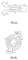
- the conductor and resistor areas are formed alternately in a circular pattern around the outside of an ink feed hole 70.
- the common and conductive trace resistor lead-in patterns 74 and 76 are formed in a tapered configuration as shown and terminate on opposite sides of the edge 76 of the polymer barrier layer defining the circular firing chamber and surrounding the circular ink feed hole 70.
- Axially aligned thermal ink jet printheads constructed in accordance with the embodiment of Figure 2D feature completely uniform coaxial heating of the ink supplied by way of the central ink feed hole 70, and also provide an additional degree of circuit design flexibility for making external connections to pulse drive circuitry for the TIJ printhead.
- photo-lithographic masking and etching processes used in TIJ printhead manufacture may be readily varied in order to change the respective areas of the resistors 66 and conductors 68 to accommodate a particular TIJ pen application.
- the X and Y conductive leads formed in the various patterns described above might be fabricated of materials other than aluminum, such as polycrystalline silicon or other metals such as tungsten.
- the areas thereof adjacent to the heater resistors can be appropriately doped with an impurity to provide P-N junctions therein and junction isolation useful for reducing leakage currents in the printhead structure.
- piezoelectric transducers may be substituted for heater resistors as will be understood by those skilled in the art.
- the present invention is not limited to the particular photolithographic thin film deposition processes described above.
- the above process may be employed with different types of thin film resistor substrate construction techniques such as, for example, those disclosed and claimed in U.S. Patent No. 4,847,630 issued to Bhaskar et al, assigned to the present assignee and incorporated herein by reference. Accordingly, these and other device and process modifications are clearly within the scope of the following appended claims.
Landscapes
- Engineering & Computer Science (AREA)
- Manufacturing & Machinery (AREA)
- Physics & Mathematics (AREA)
- Optics & Photonics (AREA)
- Particle Formation And Scattering Control In Inkjet Printers (AREA)
Applications Claiming Priority (2)
| Application Number | Priority Date | Filing Date | Title |
|---|---|---|---|
| US10431093A | 1993-08-09 | 1993-08-09 | |
| US104310 | 1993-08-09 |
Publications (2)
| Publication Number | Publication Date |
|---|---|
| EP0638424A2 true EP0638424A2 (fr) | 1995-02-15 |
| EP0638424A3 EP0638424A3 (fr) | 1996-07-31 |
Family
ID=22299811
Family Applications (1)
| Application Number | Title | Priority Date | Filing Date |
|---|---|---|---|
| EP94305204A Withdrawn EP0638424A3 (fr) | 1993-08-09 | 1994-07-15 | Tête d'impression par jet d'encre thermique et méthode de fabrication. |
Country Status (2)
| Country | Link |
|---|---|
| EP (1) | EP0638424A3 (fr) |
| JP (1) | JPH0768763A (fr) |
Cited By (6)
| Publication number | Priority date | Publication date | Assignee | Title |
|---|---|---|---|---|
| EP0794057A1 (fr) * | 1996-03-04 | 1997-09-10 | Hewlett-Packard Company | Dispositif d'écriture par jet d'encre avec élément chauffant à surface profilée |
| EP1080905A1 (fr) * | 1999-08-30 | 2001-03-07 | Hewlett-Packard Company | Générateur de gouttes à jet d'encre avec résistances fractionnées pour réduire le tassement des courants |
| EP1613477A4 (fr) * | 2003-03-25 | 2008-09-17 | Lexmark Int Inc | Tete d'impression a jet d'encre presentant une chambre a bulles a paroi convexe |
| CN100421944C (zh) * | 2004-06-25 | 2008-10-01 | 三星电子株式会社 | 具有通道阻挡器的喷墨头及其制造方法 |
| US20130286102A1 (en) * | 2011-01-31 | 2013-10-31 | Hewlett-Packard Development Company, L.P. | Fluid Ejection Device Having Firing Chamber With Contoured Floor |
| EP2681050A4 (fr) * | 2011-03-01 | 2014-10-15 | Hewlett Packard Development Co | Résistance chauffante du type annulaire pour mécanisme d'éjection de fluide thermique |
Families Citing this family (1)
| Publication number | Priority date | Publication date | Assignee | Title |
|---|---|---|---|---|
| SG152904A1 (en) * | 2000-10-20 | 2009-06-29 | Silverbrook Res Pty Ltd | Cartridge for an electronic pen |
Family Cites Families (10)
| Publication number | Priority date | Publication date | Assignee | Title |
|---|---|---|---|---|
| US3177800A (en) * | 1962-06-28 | 1965-04-13 | Sperry Rand Corp | Immersed spark gap printer |
| EP0124312A3 (fr) * | 1983-04-29 | 1985-08-28 | Hewlett-Packard Company | Structures de résistance pour imprimantes à jet d'encre thermiques |
| JPS60208246A (ja) * | 1984-04-02 | 1985-10-19 | Canon Inc | 液体噴射記録ヘツド |
| JPH0698753B2 (ja) * | 1984-10-23 | 1994-12-07 | セイコーエプソン株式会社 | インクジエツト記録装置 |
| US4580149A (en) * | 1985-02-19 | 1986-04-01 | Xerox Corporation | Cavitational liquid impact printer |
| JPS6294347A (ja) * | 1985-10-22 | 1987-04-30 | Ricoh Seiki Kk | 熱インクジエツトプリントヘツド |
| EP0367303A1 (fr) * | 1986-04-28 | 1990-05-09 | Hewlett-Packard Company | Tête d'impression à jet d'encre thermique |
| JPS63189243A (ja) * | 1987-02-02 | 1988-08-04 | Seiko Epson Corp | インクジエツト記録装置 |
| US4870433A (en) * | 1988-07-28 | 1989-09-26 | International Business Machines Corporation | Thermal drop-on-demand ink jet print head |
| JP3159272B2 (ja) * | 1992-08-04 | 2001-04-23 | ソニー株式会社 | インクジェットプリントヘッド及びインクジェットプリンタ |
-
1994
- 1994-07-15 EP EP94305204A patent/EP0638424A3/fr not_active Withdrawn
- 1994-08-09 JP JP20916294A patent/JPH0768763A/ja active Pending
Cited By (11)
| Publication number | Priority date | Publication date | Assignee | Title |
|---|---|---|---|---|
| EP0794057A1 (fr) * | 1996-03-04 | 1997-09-10 | Hewlett-Packard Company | Dispositif d'écriture par jet d'encre avec élément chauffant à surface profilée |
| US6485128B1 (en) | 1996-03-04 | 2002-11-26 | Hewlett-Packard Company | Ink jet pen with a heater element having a contoured surface |
| EP1080905A1 (fr) * | 1999-08-30 | 2001-03-07 | Hewlett-Packard Company | Générateur de gouttes à jet d'encre avec résistances fractionnées pour réduire le tassement des courants |
| US6280019B1 (en) | 1999-08-30 | 2001-08-28 | Hewlett-Packard Company | Segmented resistor inkjet drop generator with current crowding reduction |
| US6367147B2 (en) | 1999-08-30 | 2002-04-09 | Hewlett-Packard Company | Segmented resistor inkjet drop generator with current crowding reduction |
| US6422688B2 (en) | 1999-08-30 | 2002-07-23 | Hewlett-Packard Company | Segmented resistor inkjet drop generator with current crowding reduction |
| EP1613477A4 (fr) * | 2003-03-25 | 2008-09-17 | Lexmark Int Inc | Tete d'impression a jet d'encre presentant une chambre a bulles a paroi convexe |
| CN100421944C (zh) * | 2004-06-25 | 2008-10-01 | 三星电子株式会社 | 具有通道阻挡器的喷墨头及其制造方法 |
| US20130286102A1 (en) * | 2011-01-31 | 2013-10-31 | Hewlett-Packard Development Company, L.P. | Fluid Ejection Device Having Firing Chamber With Contoured Floor |
| US8783831B2 (en) * | 2011-01-31 | 2014-07-22 | Hewlett-Packard Development Company, L.P. | Fluid ejection device having firing chamber with contoured floor |
| EP2681050A4 (fr) * | 2011-03-01 | 2014-10-15 | Hewlett Packard Development Co | Résistance chauffante du type annulaire pour mécanisme d'éjection de fluide thermique |
Also Published As
| Publication number | Publication date |
|---|---|
| EP0638424A3 (fr) | 1996-07-31 |
| JPH0768763A (ja) | 1995-03-14 |
Similar Documents
| Publication | Publication Date | Title |
|---|---|---|
| US5229785A (en) | Method of manufacture of a thermal inkjet thin film printhead having a plastic orifice plate | |
| EP0271257B1 (fr) | Dispositif à résistance verticale à couche mince pour une tête imprimante à projection thermique d'encre et son procédé de fabrication | |
| EP0514706A2 (fr) | Procédé de fabrication de têtes d'impression thermique pour jet d'encre ayant des substrats métalliques et têtes d'impression réalisées par le dit procédé | |
| US5103246A (en) | X-Y multiplex drive circuit and associated ink feed connection for maximizing packing density on thermal ink jet (TIJ) printheads | |
| US6158846A (en) | Forming refill for monolithic inkjet printhead | |
| US6137443A (en) | Single-side fabrication process for forming inkjet monolithic printing element array on a substrate | |
| EP0321075B1 (fr) | Tête d'imprimante à jet d'encre intégrée et son procédé de fabrication | |
| JPH06115075A (ja) | インクジェットプリントヘッド | |
| KR100493160B1 (ko) | 테이퍼 형상의 노즐을 가진 일체형 잉크젯 프린트헤드 및그 제조방법 | |
| JP2003019798A (ja) | プリントヘッド | |
| EP0955166A1 (fr) | Tête d'impression à couche mince à jet d'encre | |
| EP1149705B1 (fr) | Tête d'impression à projection d'encre par bulles, procédé de fabrication et procédé d'éjection d'encre | |
| KR20040044281A (ko) | 두 개의 잉크챔버 사이에 배치된 히터를 가진 일체형잉크젯 프린트헤드 및 그 제조방법 | |
| KR20040049151A (ko) | 일체형 잉크젯 프린트헤드 및 그 제조방법 | |
| KR20030040689A (ko) | 잉크젯 프린트헤드 및 그 제조방법 | |
| US6926389B2 (en) | Bubble-jet type ink-jet print head and manufacturing method thereof | |
| EP0863006B1 (fr) | Film de transition carbure métallique pour application aux têtes d'impression à jet d'encre | |
| US4835553A (en) | Thermal ink jet printhead with increased drop generation rate | |
| EP0638424A2 (fr) | Tête d'impression par jet d'encre thermique et méthode de fabrication | |
| KR100552664B1 (ko) | 측벽에 의해 한정되는 잉크 챔버를 가진 일체형 잉크젯프린트헤드 및 그 제조방법 | |
| US6776915B2 (en) | Method of manufacturing a fluid ejection device with a fluid channel therethrough | |
| EP1407884B1 (fr) | Tête d'impression par jet d'encre monolithe à plaque à orifices métallique et son procédé de fabrication | |
| EP1518681B1 (fr) | Imprimante à jet d'encre | |
| KR100499132B1 (ko) | 잉크젯 프린트헤드 및 그 제조방법 | |
| JP3222148B2 (ja) | 熱インク・ジェット・プリントヘッド用多重回路付きインク供給構造および熱インク・ジェット・プリントヘッド |
Legal Events
| Date | Code | Title | Description |
|---|---|---|---|
| PUAI | Public reference made under article 153(3) epc to a published international application that has entered the european phase |
Free format text: ORIGINAL CODE: 0009012 |
|
| AK | Designated contracting states |
Kind code of ref document: A2 Designated state(s): DE FR GB IT |
|
| PUAL | Search report despatched |
Free format text: ORIGINAL CODE: 0009013 |
|
| AK | Designated contracting states |
Kind code of ref document: A3 Designated state(s): DE FR GB IT |
|
| 17P | Request for examination filed |
Effective date: 19970109 |
|
| STAA | Information on the status of an ep patent application or granted ep patent |
Free format text: STATUS: THE APPLICATION HAS BEEN WITHDRAWN |
|
| 18W | Application withdrawn |
Withdrawal date: 19971121 |