EP0636995B1 - Dispositif d'analyse de supports d'informations pourvu de moyens de compensation de ses signaux de sortie - Google Patents
Dispositif d'analyse de supports d'informations pourvu de moyens de compensation de ses signaux de sortie Download PDFInfo
- Publication number
- EP0636995B1 EP0636995B1 EP94401324A EP94401324A EP0636995B1 EP 0636995 B1 EP0636995 B1 EP 0636995B1 EP 94401324 A EP94401324 A EP 94401324A EP 94401324 A EP94401324 A EP 94401324A EP 0636995 B1 EP0636995 B1 EP 0636995B1
- Authority
- EP
- European Patent Office
- Prior art keywords
- light
- output
- source
- threshold voltage
- converter
- Prior art date
- Legal status (The legal status is an assumption and is not a legal conclusion. Google has not performed a legal analysis and makes no representation as to the accuracy of the status listed.)
- Expired - Lifetime
Links
Images


Classifications
-
- G—PHYSICS
- G06—COMPUTING OR CALCULATING; COUNTING
- G06K—GRAPHICAL DATA READING; PRESENTATION OF DATA; RECORD CARRIERS; HANDLING RECORD CARRIERS
- G06K7/00—Methods or arrangements for sensing record carriers, e.g. for reading patterns
- G06K7/10—Methods or arrangements for sensing record carriers, e.g. for reading patterns by electromagnetic radiation, e.g. optical sensing; by corpuscular radiation
- G06K7/10544—Methods or arrangements for sensing record carriers, e.g. for reading patterns by electromagnetic radiation, e.g. optical sensing; by corpuscular radiation by scanning of the records by radiation in the optical part of the electromagnetic spectrum
- G06K7/10821—Methods or arrangements for sensing record carriers, e.g. for reading patterns by electromagnetic radiation, e.g. optical sensing; by corpuscular radiation by scanning of the records by radiation in the optical part of the electromagnetic spectrum further details of bar or optical code scanning devices
- G06K7/10851—Circuits for pulse shaping, amplifying, eliminating noise signals, checking the function of the sensing device
Definitions
- the present invention relates to devices analysis of information carriers and relates more particularly to such devices used in especially for reading game reports or received in gaming terminals such as lottery, lotto, mutual betting or other games.
- the image detector generally comprises a row of light emitting diodes, the number is a function of horizontal resolution and the light intensity required.
- These diodes are associated light focusing and filtering devices intended to focus the diode beams on a transparent wall of the detector housing against which must be applied the side of the document to be analyzed which carries on the one hand fixed inscriptions such as a game grid, grid box numbers, date and other indications and on the other hand, inscriptions variables carried by the player in the grid of play as well as fixed inscriptions such as framing marks, a code relating to the type of game to which belongs the newsletter.
- a predetermined output voltage threshold Vs if the response of a photo-sensitive element is lower than Vs, it is accepted that it is on the document read from an image element or black pixel.
- the response of the photo-sensitive element is greater than the threshold Vs, the pixel considered is "white".
- US-A-38 00 078 describes a system for analyzing documents through a series of photodiodes.
- the document to be analyzed is lit by two light emitting diodes.
- the variations in sensitivity of each photodiode as well as variations in illumination are compensated by memorizing the values of the signals emitted by each photodiode when a blank page is scanned, and using these stored values to compensate the signals emitted by each photodiode during the analysis another document.
- the invention aims to create an analysis device information carriers of the aforementioned type, the response to which is as homogeneous as possible over its entire extent.
- a device for analyzing information carriers including an image detector comprising in a housing a series of light sources to shed light on the information medium to be analyzed, with which a photo-sensitive element is associated, light sources and photo-sensitive elements being arranged in two rows following the length of the image detector, the device comprising furthermore a source of threshold voltage and means for comparison of the output signals of each element photo-sensitive to the threshold voltage of said source, the device further comprising means for compensation for varying at least one of the parameters including the output voltage of each element photo-sensitive, the threshold voltage and the intensity of the light signal emitted by the associated source to obtain uniform response of all photo-sensitive elements of the reading device, said compensation means include at least one memory for storing values correction of at least one of said relative parameters each light source couple - photo-sensitive element and means for modifying said at least one parameter according to the corresponding correction values contained in said brief, and said parameters modification means include a digital to analog converter multiplier connected to the output of each photo-sensitive element and / or at the output from the threshold voltage
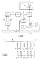
- Fig. 1 there is shown schematically a information media analysis device to which are intended to be applied the means of compensation according to the invention.
- This device mainly comprises a detector images 1 arranged opposite a drive roller 2 of a document 3 to analyze.
- Roller 2 is connected to an electric motor step by step not shown intended to allow the analysis of the document 3 by successive scan lines with a vertical resolution which is a function of the pitch adopted for moving the roller 2.
- Image detector 1 is connected to a data processing device 4 which comprises between other a comparator 5 connected between the data output of the image detector and the input of a processing unit 7 of the comparator 5 output signals, the output is connected to an input of the processing unit data 7.
- the data processing unit 7 is connected on the one hand to a control circuit not shown of the stepper motor driving roller 2 and other part, to a light intensity control circuit 8.
- the output of the control circuit 8 is connected to the image detection device 1 in the manner which will be described below.
- the image detector 1 comprises a housing 9 of parallelepiped shape in which a row is mounted of light-emitting diodes 10 of which the number is function of horizontal resolution and intensity light required.
- These diodes 10 are associated with organs 11 of focusing and filtering light intended for focus the beams 12 on a transparent wall 13 of the housing 9 of the detector against which must be applied the side of document 3 to be analyzed which in the case of a game report carries on the one hand inscriptions fixed such as a game grid, box numbers of the grid, date and other indications, printed in the color of the light emitted and which will therefore not not reproduced by the device and on the other hand, variable inscriptions carried by the player in the game board in a different color than the light emitted, as well as fixed inscriptions such as framing marks, a code relating to the type of game to which belongs the bulletin printed in one color different from that of the light emitted and which will reproduced.
- inscriptions fixed such as a game grid, box numbers of the grid, date and other indications
- the photo-sensitive elements 16 are connected each through an amplifier 17 to a input of a comparator 5 of which the other input is connected at source 6 of reference threshold voltage Vs.
- the output of the intensity control circuit 8 light is connected to light emitting diodes 10.
- the detector image has 36 light emitting diodes which are associated with 1728 photo-sensitive elements.
- the problem is that the sensitivity sets made up of light-emitting diode pairs - photo-sensitive element, is not constant.
- the circuit shown in Fig. 2 ensures such a correction.
- This circuit is interposed between the elements photo-sensitive 16 and amplifier 17 associated with comparator 5 of the data processing device 4 shown in Fig. 1.
- It basically includes a converter digital-analog 20 multiplier connected between photo-sensitive elements 16 and the aforementioned amplifier 17.
- a memory 21 such as a memory EPROM or RAM for example whose address entry is connected to a counter 22 such as an 11-bit counter by example in turn connected to a clock circuit 23 which applies signals to the reset inputs reset and CLK clock of counter 22.
- the clock circuit 23 is connected to a bus of microprocessor 24.
- the circuit also includes a circuit three-state bus control 25 connected by a conductor with eight lines between memory 21 and the converter analog-to-digital multiplier 20.
- Circuit 25 is also connected to the bus microprocessor 24.
- comparator 5 is connected to the bus microprocessor 24 which is part of the processing unit 7 (Fig. 1).
- the circuit of Fig. 2 and more particularly the digital-analog converter 20 that it has is connected between the elements photo-sensitive 16 of the image detector device 1 and comparator 5 of the output of these photo-sensitive elements with the threshold voltage Vs.
- this circuit can also be connected between source 6 of threshold voltage and input corresponding to comparator 5 or at the output of circuit 8 for controlling the light intensity of the diodes light emitting 10.
- Logic not shown programs the clock 23 so that it generates LINE CLK and PIXEL CLK signals. These signals being applied to counter 22 or more particularly at its RESET and CLK inputs, the counter proceeds at an incrementation for each pixel of the detector of images to 1728.
- the outputs of the counter which in the present example are 12 in number, make up the addresses of the memory 21 which is a RAM of 2K x 8, for example or a EPROM.
- the address of memory 21 changes and the memory sends a value to its data output digital to analog converter 20.
- the converter digital-analog multiplier performs multiplication between this stored value and the output signal of the corresponding photo-sensitive element 16. The operation above is repeated until the 1728 photo-sensitive elements 16 have been taken into account.
- An algorithm allows to load for each pixel of the image detector device in the memory 21, a compensation value allowing comparator 5 to change state when the element output signal photo-sensitive 16 associated with diodes 10 reaches the value threshold Vs delivered by the threshold voltage source 6 after this output signal has been compensated to hold account of the imprecision of response of the photo-sensitive element associated with the light emitting diode.
- the digital-to-analog converter 20 can be either a linear converter or a converter non-linear.
- the value digital to digital to analog converter is between 0/255 and 255/255, in steps of 1/255.
- This converter has an input resistance R connected between its input and its output.
- the input resistance R of the converter is connected to resistors R1, R2, R3, R4, R5 and R6 connected in parallel with interposition in series with each resistance of a controlled switch DO, D1, D2, D3, D4, D5.
- the control electrodes of DO switches to D5 of digital-analog converter 20 are connected to the corresponding data output bits B0 to B5 from memory 21.
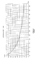
- the response curve of the analog-digital converter multiplier in Fig. 3 is shown in Fig. 4 where we see that with six resistors in parallel R1 at R6, corresponding to 6 bits of output from memory 21, there are 64 tension steps.
- the compensation means according to the invention allow to gain uniformity of response over the entire length of the image detection device.
Landscapes
- Physics & Mathematics (AREA)
- Engineering & Computer Science (AREA)
- Electromagnetism (AREA)
- General Physics & Mathematics (AREA)
- General Health & Medical Sciences (AREA)
- Artificial Intelligence (AREA)
- Computer Vision & Pattern Recognition (AREA)
- Health & Medical Sciences (AREA)
- Theoretical Computer Science (AREA)
- Toxicology (AREA)
- Facsimile Scanning Arrangements (AREA)
- Image Input (AREA)
- Holo Graphy (AREA)
- Length Measuring Devices By Optical Means (AREA)
- Measuring Pulse, Heart Rate, Blood Pressure Or Blood Flow (AREA)
- Inspection Of Paper Currency And Valuable Securities (AREA)
- Steroid Compounds (AREA)
- Photometry And Measurement Of Optical Pulse Characteristics (AREA)
- Measurement Of The Respiration, Hearing Ability, Form, And Blood Characteristics Of Living Organisms (AREA)
Priority Applications (1)
| Application Number | Priority Date | Filing Date | Title |
|---|---|---|---|
| SI9430274T SI0636995T1 (en) | 1993-06-29 | 1994-06-13 | Device for analysing information supports with means for compensating its output signals |
Applications Claiming Priority (2)
| Application Number | Priority Date | Filing Date | Title |
|---|---|---|---|
| FR9307916 | 1993-06-29 | ||
| FR9307916A FR2708118B1 (fr) | 1993-06-29 | 1993-06-29 | Dispositif d'analyse de supports d'informations pourvu de moyens de compensation de ses signaux de sortie. |
Publications (2)
| Publication Number | Publication Date |
|---|---|
| EP0636995A1 EP0636995A1 (fr) | 1995-02-01 |
| EP0636995B1 true EP0636995B1 (fr) | 1999-08-25 |
Family
ID=9448680
Family Applications (1)
| Application Number | Title | Priority Date | Filing Date |
|---|---|---|---|
| EP94401324A Expired - Lifetime EP0636995B1 (fr) | 1993-06-29 | 1994-06-13 | Dispositif d'analyse de supports d'informations pourvu de moyens de compensation de ses signaux de sortie |
Country Status (13)
| Country | Link |
|---|---|
| US (1) | US5466922A (da) |
| EP (1) | EP0636995B1 (da) |
| JP (1) | JPH07105298A (da) |
| CN (1) | CN1034095C (da) |
| AT (1) | ATE183838T1 (da) |
| AU (1) | AU685793B2 (da) |
| DE (1) | DE69420215T2 (da) |
| DK (1) | DK0636995T3 (da) |
| ES (1) | ES2136714T3 (da) |
| FR (1) | FR2708118B1 (da) |
| GR (1) | GR3031590T3 (da) |
| SI (1) | SI0636995T1 (da) |
| TW (1) | TW290671B (da) |
Families Citing this family (2)
| Publication number | Priority date | Publication date | Assignee | Title |
|---|---|---|---|---|
| FR2713802B1 (fr) * | 1993-12-13 | 1996-03-01 | Int Jeux | Procédé et dispositif d'étalonnage d'un détecteur d'images pourvu de moyens de compensation de ses signaux de sortie. |
| ATE412172T1 (de) | 2002-11-14 | 2008-11-15 | Ccs Inc | System zur einstellung der lichtintensität |
Family Cites Families (6)
| Publication number | Priority date | Publication date | Assignee | Title |
|---|---|---|---|---|
| US3800078A (en) * | 1972-12-18 | 1974-03-26 | Ibm | Digitally compensated scanning system |
| JPS54132131A (en) * | 1978-04-05 | 1979-10-13 | Sumitomo Electric Ind Ltd | Optical information reading device |
| DE3409818A1 (de) * | 1984-03-16 | 1985-09-26 | Siemens AG, 1000 Berlin und 8000 München | Optoelektronisches abtastsystem mit automatischem abgleich |
| US4647981A (en) * | 1984-10-25 | 1987-03-03 | Xerox Corporation | Automatic white level control for a RIS |
| US5032712A (en) * | 1988-10-19 | 1991-07-16 | Canon Kabushiki Kaisha | Signal accumulation image reading apparatus |
| US5189290A (en) * | 1989-10-14 | 1993-02-23 | Omron Corporation | Optical card processing apparatus using tracking error signals to determine proper card orientation |
-
1993
- 1993-06-29 FR FR9307916A patent/FR2708118B1/fr not_active Expired - Lifetime
-
1994
- 1994-06-13 AT AT94401324T patent/ATE183838T1/de not_active IP Right Cessation
- 1994-06-13 DK DK94401324T patent/DK0636995T3/da active
- 1994-06-13 EP EP94401324A patent/EP0636995B1/fr not_active Expired - Lifetime
- 1994-06-13 US US08/258,865 patent/US5466922A/en not_active Expired - Fee Related
- 1994-06-13 DE DE69420215T patent/DE69420215T2/de not_active Expired - Fee Related
- 1994-06-13 SI SI9430274T patent/SI0636995T1/xx not_active IP Right Cessation
- 1994-06-13 ES ES94401324T patent/ES2136714T3/es not_active Expired - Lifetime
- 1994-06-15 AU AU64745/94A patent/AU685793B2/en not_active Ceased
- 1994-06-25 TW TW083105778A patent/TW290671B/zh active
- 1994-06-28 CN CN94107945A patent/CN1034095C/zh not_active Expired - Fee Related
- 1994-06-29 JP JP6147745A patent/JPH07105298A/ja active Pending
-
1999
- 1999-10-21 GR GR990402684T patent/GR3031590T3/el unknown
Also Published As
| Publication number | Publication date |
|---|---|
| CN1111376A (zh) | 1995-11-08 |
| JPH07105298A (ja) | 1995-04-21 |
| ATE183838T1 (de) | 1999-09-15 |
| SI0636995T1 (en) | 1999-12-31 |
| CN1034095C (zh) | 1997-02-19 |
| EP0636995A1 (fr) | 1995-02-01 |
| ES2136714T3 (es) | 1999-12-01 |
| US5466922A (en) | 1995-11-14 |
| AU685793B2 (en) | 1998-01-29 |
| TW290671B (da) | 1996-11-11 |
| DE69420215D1 (de) | 1999-09-30 |
| FR2708118B1 (fr) | 1995-10-06 |
| FR2708118A1 (fr) | 1995-01-27 |
| AU6474594A (en) | 1995-01-12 |
| DK0636995T3 (da) | 2000-03-06 |
| DE69420215T2 (de) | 1999-12-09 |
| GR3031590T3 (en) | 2000-01-31 |
Similar Documents
| Publication | Publication Date | Title |
|---|---|---|
| EP0306362B1 (fr) | Equipement d'acquisition et de traitement de données pour le contrôle de véhicules automobiles | |
| FR2490351A1 (fr) | Appareil d'etalonnage pour convertisseurs analogiques numeriques | |
| FR2588656A1 (fr) | Appareil de spectro-colorimetrie a fibres optiques | |
| US4347533A (en) | Facsimile reading and recording device | |
| EP0349415A1 (fr) | Procédé et dispositif de commande d'un écran matriciel affichant des niveaux de gris | |
| FR2703453A1 (fr) | Codeur de valeur absolue et procédé de correction de sortie d'un codeur de valeur absolue. | |
| EP0028957A1 (fr) | Dispositif de restitution de nuances utilisant une tête d'impression thermique et système d'impression thermique comportant un tel dispositif | |
| CH668127A5 (fr) | Dispositiv de mesure de densite optique/pourcentage de points. | |
| FR2580068A1 (da) | ||
| EP0636995A1 (fr) | Dispositif d'analyse de supports d'informations pourvu de moyens de compensation de ses signaux de sortie | |
| US4984285A (en) | Method of correcting shading phenomenon in optical character reader | |
| JP2748263B2 (ja) | バーコードリーダと、それに用いるイメージセンサ | |
| EP0348792A1 (fr) | Procédé et dispositif de traitement de signaux électriques provenant de l'analyse d'une ligne d'une image | |
| CA2077147C (fr) | Procede et dispositif de commande d'un convertisseur de longueur d'onde optique | |
| JP2725508B2 (ja) | 多素子光センサ装置 | |
| FR2661529A1 (fr) | Dispositif de traitement d'imprimes comportant des cases a completer, notamment des bulletins de loterie. | |
| EP0045252A2 (fr) | Dispositif de lecture ou de restitution d'un document, en particulier pour appareil de télécopie | |
| EP0118919A2 (en) | Method and apparatus for converting spectral and light intensity values directly to digital data | |
| EP0657837B1 (fr) | Procédé et dispositif d'étalonnage d'un détecteur d'images pourvu de moyens de compensation de ses signaux de sortie | |
| JP2005323103A (ja) | 画像読取装置 | |
| JP3739661B2 (ja) | 画像読取装置 | |
| JPS58223964A (ja) | シエ−デイング補正装置 | |
| JPH0898017A (ja) | イメージセンサの出力レベル補正装置 | |
| EP0206900B1 (fr) | Dispositif de lecture de code optique, notamment du type entièrement intégré | |
| EP0500481B1 (fr) | Circuit et procédé de sélection des k plus grandes données d'une suite de données |
Legal Events
| Date | Code | Title | Description |
|---|---|---|---|
| PUAI | Public reference made under article 153(3) epc to a published international application that has entered the european phase |
Free format text: ORIGINAL CODE: 0009012 |
|
| AK | Designated contracting states |
Kind code of ref document: A1 Designated state(s): AT BE CH DE DK ES FR GB GR IE IT LI LU MC NL PT SE |
|
| RAX | Requested extension states of the european patent have changed |
Free format text: SI PAYMENT 940621 |
|
| 17P | Request for examination filed |
Effective date: 19950728 |
|
| 17Q | First examination report despatched |
Effective date: 19980209 |
|
| GRAG | Despatch of communication of intention to grant |
Free format text: ORIGINAL CODE: EPIDOS AGRA |
|
| GRAG | Despatch of communication of intention to grant |
Free format text: ORIGINAL CODE: EPIDOS AGRA |
|
| GRAH | Despatch of communication of intention to grant a patent |
Free format text: ORIGINAL CODE: EPIDOS IGRA |
|
| GRAH | Despatch of communication of intention to grant a patent |
Free format text: ORIGINAL CODE: EPIDOS IGRA |
|
| GRAA | (expected) grant |
Free format text: ORIGINAL CODE: 0009210 |
|
| AK | Designated contracting states |
Kind code of ref document: B1 Designated state(s): AT BE CH DE DK ES FR GB GR IE IT LI LU MC NL PT SE |
|
| AX | Request for extension of the european patent |
Free format text: SI PAYMENT 19940621 |
|
| REF | Corresponds to: |
Ref document number: 183838 Country of ref document: AT Date of ref document: 19990915 Kind code of ref document: T |
|
| REG | Reference to a national code |
Ref country code: CH Ref legal event code: EP |
|
| GBT | Gb: translation of ep patent filed (gb section 77(6)(a)/1977) |
Effective date: 19990827 |
|
| REF | Corresponds to: |
Ref document number: 69420215 Country of ref document: DE Date of ref document: 19990930 |
|
| REG | Reference to a national code |
Ref country code: IE Ref legal event code: FG4D Free format text: FRENCH |
|
| REG | Reference to a national code |
Ref country code: ES Ref legal event code: FG2A Ref document number: 2136714 Country of ref document: ES Kind code of ref document: T3 |
|
| REG | Reference to a national code |
Ref country code: PT Ref legal event code: SC4A Free format text: AVAILABILITY OF NATIONAL TRANSLATION Effective date: 19991102 |
|
| REG | Reference to a national code |
Ref country code: DK Ref legal event code: T3 |
|
| PLBE | No opposition filed within time limit |
Free format text: ORIGINAL CODE: 0009261 |
|
| STAA | Information on the status of an ep patent application or granted ep patent |
Free format text: STATUS: NO OPPOSITION FILED WITHIN TIME LIMIT |
|
| 26N | No opposition filed | ||
| REG | Reference to a national code |
Ref country code: GB Ref legal event code: IF02 |
|
| PGFP | Annual fee paid to national office [announced via postgrant information from national office to epo] |
Ref country code: CH Payment date: 20030515 Year of fee payment: 10 Ref country code: AT Payment date: 20030515 Year of fee payment: 10 |
|
| PGFP | Annual fee paid to national office [announced via postgrant information from national office to epo] |
Ref country code: MC Payment date: 20030519 Year of fee payment: 10 Ref country code: LU Payment date: 20030519 Year of fee payment: 10 Ref country code: DK Payment date: 20030519 Year of fee payment: 10 |
|
| PGFP | Annual fee paid to national office [announced via postgrant information from national office to epo] |
Ref country code: SE Payment date: 20030520 Year of fee payment: 10 Ref country code: NL Payment date: 20030520 Year of fee payment: 10 |
|
| PGFP | Annual fee paid to national office [announced via postgrant information from national office to epo] |
Ref country code: GR Payment date: 20030529 Year of fee payment: 10 |
|
| PGFP | Annual fee paid to national office [announced via postgrant information from national office to epo] |
Ref country code: IE Payment date: 20030603 Year of fee payment: 10 |
|
| PGFP | Annual fee paid to national office [announced via postgrant information from national office to epo] |
Ref country code: GB Payment date: 20030606 Year of fee payment: 10 |
|
| PGFP | Annual fee paid to national office [announced via postgrant information from national office to epo] |
Ref country code: DE Payment date: 20030611 Year of fee payment: 10 |
|
| PGFP | Annual fee paid to national office [announced via postgrant information from national office to epo] |
Ref country code: ES Payment date: 20030612 Year of fee payment: 10 |
|
| PGFP | Annual fee paid to national office [announced via postgrant information from national office to epo] |
Ref country code: FR Payment date: 20030616 Year of fee payment: 10 |
|
| PGFP | Annual fee paid to national office [announced via postgrant information from national office to epo] |
Ref country code: PT Payment date: 20030625 Year of fee payment: 10 |
|
| PGFP | Annual fee paid to national office [announced via postgrant information from national office to epo] |
Ref country code: BE Payment date: 20030709 Year of fee payment: 10 |
|
| PG25 | Lapsed in a contracting state [announced via postgrant information from national office to epo] |
Ref country code: LU Free format text: LAPSE BECAUSE OF NON-PAYMENT OF DUE FEES Effective date: 20040613 Ref country code: GB Free format text: LAPSE BECAUSE OF NON-PAYMENT OF DUE FEES Effective date: 20040613 Ref country code: AT Free format text: LAPSE BECAUSE OF NON-PAYMENT OF DUE FEES Effective date: 20040613 |
|
| PG25 | Lapsed in a contracting state [announced via postgrant information from national office to epo] |
Ref country code: SE Free format text: LAPSE BECAUSE OF NON-PAYMENT OF DUE FEES Effective date: 20040614 Ref country code: IE Free format text: LAPSE BECAUSE OF NON-PAYMENT OF DUE FEES Effective date: 20040614 Ref country code: ES Free format text: LAPSE BECAUSE OF NON-PAYMENT OF DUE FEES Effective date: 20040614 |
|
| PG25 | Lapsed in a contracting state [announced via postgrant information from national office to epo] |
Ref country code: MC Free format text: LAPSE BECAUSE OF NON-PAYMENT OF DUE FEES Effective date: 20040630 Ref country code: LI Free format text: LAPSE BECAUSE OF NON-PAYMENT OF DUE FEES Effective date: 20040630 Ref country code: DK Free format text: LAPSE BECAUSE OF NON-PAYMENT OF DUE FEES Effective date: 20040630 Ref country code: CH Free format text: LAPSE BECAUSE OF NON-PAYMENT OF DUE FEES Effective date: 20040630 Ref country code: BE Free format text: LAPSE BECAUSE OF NON-PAYMENT OF DUE FEES Effective date: 20040630 |
|
| PG25 | Lapsed in a contracting state [announced via postgrant information from national office to epo] |
Ref country code: PT Free format text: LAPSE BECAUSE OF NON-PAYMENT OF DUE FEES Effective date: 20041213 |
|
| BERE | Be: lapsed |
Owner name: *INTERNATIONALE DES JEUX Effective date: 20040630 |
|
| PG25 | Lapsed in a contracting state [announced via postgrant information from national office to epo] |
Ref country code: NL Free format text: LAPSE BECAUSE OF NON-PAYMENT OF DUE FEES Effective date: 20050101 Ref country code: DE Free format text: LAPSE BECAUSE OF NON-PAYMENT OF DUE FEES Effective date: 20050101 |
|
| PG25 | Lapsed in a contracting state [announced via postgrant information from national office to epo] |
Ref country code: GR Free format text: LAPSE BECAUSE OF NON-PAYMENT OF DUE FEES Effective date: 20050105 |
|
| REG | Reference to a national code |
Ref country code: DK Ref legal event code: EBP |
|
| EUG | Se: european patent has lapsed | ||
| GBPC | Gb: european patent ceased through non-payment of renewal fee |
Effective date: 20040613 |
|
| EUG | Se: european patent has lapsed | ||
| REG | Reference to a national code |
Ref country code: CH Ref legal event code: PL |
|
| PG25 | Lapsed in a contracting state [announced via postgrant information from national office to epo] |
Ref country code: FR Free format text: LAPSE BECAUSE OF NON-PAYMENT OF DUE FEES Effective date: 20050228 |
|
| REG | Reference to a national code |
Ref country code: PT Ref legal event code: MM4A Free format text: LAPSE DUE TO NON-PAYMENT OF FEES Effective date: 20041213 |
|
| NLV4 | Nl: lapsed or anulled due to non-payment of the annual fee |
Effective date: 20050101 |
|
| REG | Reference to a national code |
Ref country code: IE Ref legal event code: MM4A |
|
| REG | Reference to a national code |
Ref country code: FR Ref legal event code: ST |
|
| PG25 | Lapsed in a contracting state [announced via postgrant information from national office to epo] |
Ref country code: IT Free format text: LAPSE BECAUSE OF NON-PAYMENT OF DUE FEES;WARNING: LAPSES OF ITALIAN PATENTS WITH EFFECTIVE DATE BEFORE 2007 MAY HAVE OCCURRED AT ANY TIME BEFORE 2007. THE CORRECT EFFECTIVE DATE MAY BE DIFFERENT FROM THE ONE RECORDED. Effective date: 20050613 |
|
| REG | Reference to a national code |
Ref country code: ES Ref legal event code: FD2A Effective date: 20040614 |