EP0635801B1 - External storage device - Google Patents
External storage device Download PDFInfo
- Publication number
- EP0635801B1 EP0635801B1 EP94301680A EP94301680A EP0635801B1 EP 0635801 B1 EP0635801 B1 EP 0635801B1 EP 94301680 A EP94301680 A EP 94301680A EP 94301680 A EP94301680 A EP 94301680A EP 0635801 B1 EP0635801 B1 EP 0635801B1
- Authority
- EP
- European Patent Office
- Prior art keywords
- storage device
- external storage
- device main
- main assembly
- unit assembly
- Prior art date
- Legal status (The legal status is an assumption and is not a legal conclusion. Google has not performed a legal analysis and makes no representation as to the accuracy of the status listed.)
- Expired - Lifetime
Links
Images


Classifications
-
- G—PHYSICS
- G06—COMPUTING; CALCULATING OR COUNTING
- G06F—ELECTRIC DIGITAL DATA PROCESSING
- G06F13/00—Interconnection of, or transfer of information or other signals between, memories, input/output devices or central processing units
-
- G—PHYSICS
- G06—COMPUTING; CALCULATING OR COUNTING
- G06K—GRAPHICAL DATA READING; PRESENTATION OF DATA; RECORD CARRIERS; HANDLING RECORD CARRIERS
- G06K19/00—Record carriers for use with machines and with at least a part designed to carry digital markings
- G06K19/06—Record carriers for use with machines and with at least a part designed to carry digital markings characterised by the kind of the digital marking, e.g. shape, nature, code
- G06K19/067—Record carriers with conductive marks, printed circuits or semiconductor circuit elements, e.g. credit or identity cards also with resonating or responding marks without active components
- G06K19/07—Record carriers with conductive marks, printed circuits or semiconductor circuit elements, e.g. credit or identity cards also with resonating or responding marks without active components with integrated circuit chips
- G06K19/077—Constructional details, e.g. mounting of circuits in the carrier
- G06K19/07745—Mounting details of integrated circuit chips
- G06K19/07747—Mounting details of integrated circuit chips at least one of the integrated circuit chips being mounted as a module
-
- G—PHYSICS
- G06—COMPUTING; CALCULATING OR COUNTING
- G06K—GRAPHICAL DATA READING; PRESENTATION OF DATA; RECORD CARRIERS; HANDLING RECORD CARRIERS
- G06K19/00—Record carriers for use with machines and with at least a part designed to carry digital markings
- G06K19/06—Record carriers for use with machines and with at least a part designed to carry digital markings characterised by the kind of the digital marking, e.g. shape, nature, code
- G06K19/067—Record carriers with conductive marks, printed circuits or semiconductor circuit elements, e.g. credit or identity cards also with resonating or responding marks without active components
- G06K19/07—Record carriers with conductive marks, printed circuits or semiconductor circuit elements, e.g. credit or identity cards also with resonating or responding marks without active components with integrated circuit chips
- G06K19/077—Constructional details, e.g. mounting of circuits in the carrier
- G06K19/07737—Constructional details, e.g. mounting of circuits in the carrier the record carrier consisting of two or more mechanically separable parts
- G06K19/07741—Constructional details, e.g. mounting of circuits in the carrier the record carrier consisting of two or more mechanically separable parts comprising a first part operating as a regular record carrier and a second attachable part that changes the functional appearance of said record carrier, e.g. a contact-based smart card with an adapter part which, when attached to the contact card makes the contact card function as a non-contact card
-
- G—PHYSICS
- G06—COMPUTING; CALCULATING OR COUNTING
- G06K—GRAPHICAL DATA READING; PRESENTATION OF DATA; RECORD CARRIERS; HANDLING RECORD CARRIERS
- G06K19/00—Record carriers for use with machines and with at least a part designed to carry digital markings
- G06K19/06—Record carriers for use with machines and with at least a part designed to carry digital markings characterised by the kind of the digital marking, e.g. shape, nature, code
- G06K19/067—Record carriers with conductive marks, printed circuits or semiconductor circuit elements, e.g. credit or identity cards also with resonating or responding marks without active components
- G06K19/07—Record carriers with conductive marks, printed circuits or semiconductor circuit elements, e.g. credit or identity cards also with resonating or responding marks without active components with integrated circuit chips
- G06K19/077—Constructional details, e.g. mounting of circuits in the carrier
- G06K19/07743—External electrical contacts
-
- G—PHYSICS
- G06—COMPUTING; CALCULATING OR COUNTING
- G06K—GRAPHICAL DATA READING; PRESENTATION OF DATA; RECORD CARRIERS; HANDLING RECORD CARRIERS
- G06K19/00—Record carriers for use with machines and with at least a part designed to carry digital markings
- G06K19/06—Record carriers for use with machines and with at least a part designed to carry digital markings characterised by the kind of the digital marking, e.g. shape, nature, code
- G06K19/067—Record carriers with conductive marks, printed circuits or semiconductor circuit elements, e.g. credit or identity cards also with resonating or responding marks without active components
- G06K19/07—Record carriers with conductive marks, printed circuits or semiconductor circuit elements, e.g. credit or identity cards also with resonating or responding marks without active components with integrated circuit chips
- G06K19/077—Constructional details, e.g. mounting of circuits in the carrier
- G06K19/07745—Mounting details of integrated circuit chips
-
- G—PHYSICS
- G06—COMPUTING; CALCULATING OR COUNTING
- G06K—GRAPHICAL DATA READING; PRESENTATION OF DATA; RECORD CARRIERS; HANDLING RECORD CARRIERS
- G06K7/00—Methods or arrangements for sensing record carriers, e.g. for reading patterns
- G06K7/0013—Methods or arrangements for sensing record carriers, e.g. for reading patterns by galvanic contacts, e.g. card connectors for ISO-7816 compliant smart cards or memory cards, e.g. SD card readers
- G06K7/0021—Methods or arrangements for sensing record carriers, e.g. for reading patterns by galvanic contacts, e.g. card connectors for ISO-7816 compliant smart cards or memory cards, e.g. SD card readers for reading/sensing record carriers having surface contacts
-
- H—ELECTRICITY
- H01—ELECTRIC ELEMENTS
- H01L—SEMICONDUCTOR DEVICES NOT COVERED BY CLASS H10
- H01L2224/00—Indexing scheme for arrangements for connecting or disconnecting semiconductor or solid-state bodies and methods related thereto as covered by H01L24/00
- H01L2224/01—Means for bonding being attached to, or being formed on, the surface to be connected, e.g. chip-to-package, die-attach, "first-level" interconnects; Manufacturing methods related thereto
- H01L2224/42—Wire connectors; Manufacturing methods related thereto
- H01L2224/47—Structure, shape, material or disposition of the wire connectors after the connecting process
- H01L2224/48—Structure, shape, material or disposition of the wire connectors after the connecting process of an individual wire connector
- H01L2224/4805—Shape
- H01L2224/4809—Loop shape
- H01L2224/48091—Arched
-
- H—ELECTRICITY
- H01—ELECTRIC ELEMENTS
- H01L—SEMICONDUCTOR DEVICES NOT COVERED BY CLASS H10
- H01L2224/00—Indexing scheme for arrangements for connecting or disconnecting semiconductor or solid-state bodies and methods related thereto as covered by H01L24/00
- H01L2224/01—Means for bonding being attached to, or being formed on, the surface to be connected, e.g. chip-to-package, die-attach, "first-level" interconnects; Manufacturing methods related thereto
- H01L2224/42—Wire connectors; Manufacturing methods related thereto
- H01L2224/47—Structure, shape, material or disposition of the wire connectors after the connecting process
- H01L2224/48—Structure, shape, material or disposition of the wire connectors after the connecting process of an individual wire connector
- H01L2224/481—Disposition
- H01L2224/48151—Connecting between a semiconductor or solid-state body and an item not being a semiconductor or solid-state body, e.g. chip-to-substrate, chip-to-passive
- H01L2224/48221—Connecting between a semiconductor or solid-state body and an item not being a semiconductor or solid-state body, e.g. chip-to-substrate, chip-to-passive the body and the item being stacked
- H01L2224/48225—Connecting between a semiconductor or solid-state body and an item not being a semiconductor or solid-state body, e.g. chip-to-substrate, chip-to-passive the body and the item being stacked the item being non-metallic, e.g. insulating substrate with or without metallisation
- H01L2224/48227—Connecting between a semiconductor or solid-state body and an item not being a semiconductor or solid-state body, e.g. chip-to-substrate, chip-to-passive the body and the item being stacked the item being non-metallic, e.g. insulating substrate with or without metallisation connecting the wire to a bond pad of the item
-
- H—ELECTRICITY
- H01—ELECTRIC ELEMENTS
- H01L—SEMICONDUCTOR DEVICES NOT COVERED BY CLASS H10
- H01L2924/00—Indexing scheme for arrangements or methods for connecting or disconnecting semiconductor or solid-state bodies as covered by H01L24/00
- H01L2924/01—Chemical elements
- H01L2924/01078—Platinum [Pt]
-
- H—ELECTRICITY
- H01—ELECTRIC ELEMENTS
- H01L—SEMICONDUCTOR DEVICES NOT COVERED BY CLASS H10
- H01L2924/00—Indexing scheme for arrangements or methods for connecting or disconnecting semiconductor or solid-state bodies as covered by H01L24/00
- H01L2924/01—Chemical elements
- H01L2924/01079—Gold [Au]
Definitions
- the present invention relates to this external storage devices that are releasably or exchangeably used for storage equipment and external storage medium devices.
- floppy disks Two types of storage devices, or memory elements, that are capable of recording and saving various data have been utilized.
- One is incorporated and fixed within storage equipment or devices, and the other is releasably or exchangeably incorporated in storage equipment or devices.
- the external storage device for example, a floppy disk can freely be attached or detached by a one touch operation.
- the floppy disks being storage mediums, can separately be used depending on purpose and object. This therefore produces easier data reduction with optional classification, recording, and saving.
- the data occasionally disappears when recording or saving the data to produce the disadvantage of less reliability.
- Second, the floppy disk has a slow access time.
- IC memory cards comprise a functional circuit in which circuit components containing semiconductor memory devices or elements are mounted on a substrate.
- a resin case incorporates the functional circuit as an inside attachment.
- a cover covers and seals an opening surface of the resin case, and external connection terminals, such as two piece connectors, are attached on one edge of the resin case and electrically connect the functional circuit and the storage equipment.
- IC memory cards are assembled with a large number of components and parts.
- a relatively complicated structure is required impacting the thickness of the IC memory card, resulting in difficulty in realizing a compact size.
- disadvantages arise in practical use because of lower cost performance and production yields in mass producing, in addition to the decreased releasability or fluctuated releasability to the storage equipment and device.
- FR-A-2 686 172 discloses an IC card processing assembly being capable of receiving an IC card containing a non-volatile semiconductor memory device and a flat type connection terminal formed on a surface of the IC card, the processing assembly comprising:
- An object of the present invention is to provide an external storage device having a simplified structure with satisfactory production yields.
- Another object of the present invention is to provide an external storage device with a high reliability with respect to recording and saving the data.
- Another object of the present invention is to provide an external storage device having a rapid access time.
- Still another object of the present invention is to provide an external storage device having high releasability for the storage equipment and device.
- the external storage device comprises an external storage device main and an external storage device unit.
- the external storage device main includes a thin external storage device module formed into a package sealed on one side from a storage element containing at least one non-volatile semiconductor memory device, and a flat type external connection terminal connected to an input/output terminal of the storage element and led and exposed to a backside of the external storage device module.
- the external storage device unit includes a mechanism for engaging, insertedly attaching, and detaching the external storage device main, a resilient contact electrically connecting to the flat type external connection terminal of the external storage device main.
- the external storage device main may preferably be formed into a package structure sealed on one side.
- the external storage device main may also preferably be in the form of a card type structure attached on a supporting plate.
- the external storage device unit may preferably be assembled and incorporated with a part of or all of the control circuit components or parts, such as semiconductor elements, performing the control function.
- the external storage device of a preferred embodiment has a higher integration with a memory capacity to an extent of 16 M-bits per chip.
- the storage device is preferably provided as a main memory with a non-volatile semiconductor memory device which does not require a power supply for maintaining storage.
- the main memory is incorporated into the package sealed on one side to produce a thin type external storage device module or external storage device main.
- the external storage device module is easily achieved in a thin structure and at a lower cost by for example, a transfer mold system.
- an insertion system at the side surface of the external storage device unit may be provided.
- An external connection terminal is led and positioned in a plane with a rear-side of the external storage device main.
- the external storage device unit In a card type device, the external storage device itself maintains and exhibits satisfactory releasability for the storage equipment and devices.
- the card type external storage device main can readily be attached and detached to the external storage device unit, and realizes a function equivalent to a floppy disk device, and simultaneously a reliability of electrical connecting and disconnecting due to the attaching and detaching.
- Fig. 1 is a top perspective view of a first example of an external storage device main according to the present invention.
- Fig. 2 is a bottom perspective view of the first example of an external storage device main shown in Fig. 1.
- Fig. 3 is an enlarged sectional view taken along the line III-III of Fig. 1.
- Fig. 4 is a top perspective view of a second example of an external storage device main according to the present invention.
- Fig. 5 is an enlarged sectional view taken along line V-V of Fig. 4.
- Fig. 6 is a plan view of an example of an external storage device in which the external storage device main shown in Fig. 4 is assembled onto an external storage device unit.
- Fig. 7 is a sectional view taken along line VII-VII of Fig. 6.
- Fig. 8 is a plan view of an example of another external storage device in which the external storage device main shown in Fig. 7 is assembled into an external storage device unit.
- Fig. 9 is a sectional view taken along line IX-IX of Fig. 8.
- the present invention has been achieved by means of a cleverly conceived structure and profile where the devices such as semiconductor memory devices or elements are mounted on the conventional substrates and in accordance with the fact that a non-volatile semiconductor memory device or element with a capacity of 16 M-bits per chip corresponds to a 2 M-byte floppy disk.
- Figs. 1 to 3 show a first example of an external storage device module constituting features of the thin type external storage device main according to the invention, where Fig. 1 is a perspective view on one-side surface which is sealed on one side by a transfer mold, Fig. 2 is a perspective view of a rear-side surface which is one-side sealed by the transfer mold, and Fig. 3 is a sectional view taken along line III-III of Fig. 1.
- a card type external storage device module is constructed such that a storage element 2, such as a 16 M-bit NAND flash type non-volatile semiconductor memory device, is connected on a surface of the through hole type resin based wiring substrate 3 by wire-bonding 4.
- the storage element 2 may, if required, included an anti-electrostatic element for preventing electrostatic destruction, the anti-electrostatic element being used for input and output to the memory element.
- flip chip bonding may also be performed to directly adhere the rear side of the memory element 2 on the resin based wiring substrate 3.
- the substrate 3 is preferably a thin wiring substrate, for example, an insulative substrate member made of glass-epoxy resin or the like.
- the transfer mold layer 5 may generally be formed of epoxy based resin or the like. However, it also may preferably be formed of a composition containing inorganics.
- the one-side sealed through hole type resin based wiring substrate 3 in other words, the backside surface 1a of the external storage device module 1 is arranged with a plane shaped or flat type terminal 1b taken out through the through hole to form the external storage device module 1.
- the plane shaped terminal 1b is preferably gold (Au)-plated on its surface, and functions as an external connection terminal for electrically connecting to a contact member of an external storage device unit which is described later.
- the plane shaped terminal 1b is gold-plated to increase the reliability of the electrical connection. However, such plating is not always required.
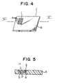
- Figs. 4 and 5 show a second structural example of the structure of a card type external storage device main 1' in which the external storage device module is attached on a card shaped supporter 6, wherein Fig. 4 is a perspective view, and Fig. 5 is a sectional view taken along line V-V of Fig. 4.
- the card shaped supporter 6 may preferably be, for example, an insulative resin plate.
- the external storage device module 1 is incorporated into the card shaped supporter 6 having a length of 42.8 mm, a width of less than 27 mm, and a thickness of 0.76 mm, wherein the size of the supporter 6 is half the card size regulated in accordance with JEIDA.
- the external storage device module 1 is assembled into the card shaped supporter 6.
- the supporter 6 has a recessed portion in which the external storage device module 1 can be inserted and attached. As shown in Figs. 4 and 5, a surface of the external connection terminal 1b of the external storage device module 1 is inserted, attached and exposed in the same plane as a main surface of the card shaped supporter 6, thereby forming the card type storage device main 1'.
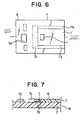
- Figs. 6 and 7 show a structural example wherein the card type external storage device main 1' is attached to an external storage device unit 7, where Fig. 6 is a plan view, and Fig. 7 is a sectional view taken along line VII-VII of Fig. 6.
- the card type external storage device main 1' has storage elements on one side thereof.
- the card type external storage device main 1' is releasably attached on and installed into the external storage device unit 7 to form an external storage device 8.
- the external storage device unit 7 can be electrically connected to the plane shaped external connection terminal 1b provided on the external storage device module 1 on the card type external storage device main 1'. Simultaneously the external storage device unit 7 has a structure that the card type external storage device main 1' is releasably attached therefrom.
- the external storage device unit 7 has on its surface a recessed portion corresponding to the shape and dimensions of the card type external storage device main 1'. A surface on the recessed portion is arranged with a contact 7a that preferably corresponds to the external connection terminal 1b of the card type external storage device main 1'.
- a guide structure 7b and a one touch structure 7c are preferably provided.
- the one touch structure 7c is preferably placed at a tip end of card 1 and provides secure attaching, electrical connection, and release thereof.
- a micro-switch system for supplying electricity to the card type external storage device main 1' may preferably be provided with the one touch structure 7c.
- 7d represents an IC element group constituting a part of a drive and control circuit for the storage element 2, including the non-volatile semiconductor memory chip, which the card type external storage device section 1' possess.
- the contact 7a for electrically connecting to the external connection terminal 1b is made, for example, using a pin-type contact having a spring mechanism.
- the external storage device 8, including the card type external storage device main 1', according to the present invention is not limited to the example as described above.
- the present invention also includes the structure shown in a plan view of Fig. 8 and in a sectional view of Fig. 9 taken along line IX-IX of Fig. 8.
- the card type external storage device main 1' may preferably be inserted or extracted from a side-surface of a case 9.
- the case 9 preferably has on one side a pin connection 9a.
- the case 9 may, for example, be sized to have a length of 85.6 mm, a width of 54.0 mm, and a thickness of 3.3 mm.
- the case 9 is also preferably provided with an insertion and extraction section 9b, such as a space or gap, for attaching, through inserting and extracting, the card type external storage device main 1' from the side-surface of the case 9.
- a push button 9c may preferably be provided on the case 9 to achieve attaching or detaching to the external storage device unit 7.
- the card type external storage device main 1' is attached by inserting and extracting from the side surface of the external storage device unit 7, compared to a structure having a surface recessed portion for attaching the card type external storage device main 1', it is correspondingly not required to enlarge an outer surface required for attaching the external storage device.
- this easily realizes a compact size, fine view, and high reliability due to incorporation (inside mount) of the card type external storage device main 1'.
- the present invention is not limited to the examples as hereinbefore described.
- the card type external storage device main 1 according to the present invention may be used, as it is, without attaching it on or to the card shaped supporter 6.
- the external storage device has a higher integration and provides, even in one chip, a larger memory capacity of a non-volatile semiconductor memory device as a main memory.
- basic construction is employed in that the external storage device main has a compact structure and the main memory is sealed on one side by a transfer mold.
- the use of the one-side sealing system and the non-volatile semiconductor memory device provides a thin structure and compact size of the external storage device.
- the releasable attaching and ease of carrying provide simple operation and handling, and result in a lower cost.
Description
- The present invention relates to this external storage devices that are releasably or exchangeably used for storage equipment and external storage medium devices.
- Two types of storage devices, or memory elements, that are capable of recording and saving various data have been utilized. One is incorporated and fixed within storage equipment or devices, and the other is releasably or exchangeably incorporated in storage equipment or devices. In the latter type, the external storage device, for example, a floppy disk can freely be attached or detached by a one touch operation. The floppy disks, being storage mediums, can separately be used depending on purpose and object. This therefore produces easier data reduction with optional classification, recording, and saving. However, a problem arises in the floppy disks described. First, the data occasionally disappears when recording or saving the data to produce the disadvantage of less reliability. Second, the floppy disk has a slow access time. Also, when employing smaller sized floppy disks in response to a miniaturization goal, the storage area of the storage medium is correspondingly smaller thereby reducing storage capacity. This results in an adverse effect in realizing both the compact size and high capacity. On the other hand, in semiconductor memory devices used as an external storage device, such as IC memory cards, the problems of floppy disks, such as low reliability on recording and saving data and slow access time, can largely be overcome. In general, IC memory cards comprise a functional circuit in which circuit components containing semiconductor memory devices or elements are mounted on a substrate. A resin case incorporates the functional circuit as an inside attachment. A cover covers and seals an opening surface of the resin case, and external connection terminals, such as two piece connectors, are attached on one edge of the resin case and electrically connect the functional circuit and the storage equipment.
- However, IC memory cards are assembled with a large number of components and parts. Thus, a relatively complicated structure is required impacting the thickness of the IC memory card, resulting in difficulty in realizing a compact size. Further, disadvantages arise in practical use because of lower cost performance and production yields in mass producing, in addition to the decreased releasability or fluctuated releasability to the storage equipment and device.
- FR-A-2 686 172 discloses an IC card processing assembly being capable of receiving an IC card containing a non-volatile semiconductor memory device and a flat type connection terminal formed on a surface of the IC card, the processing assembly comprising:
- means for engaging the IC card;
- a contact electrically connecting to the connection terminal of the IC card; and
- means for controlling data exchange with the IC card.
-
- An object of the present invention is to provide an external storage device having a simplified structure with satisfactory production yields.
- Another object of the present invention is to provide an external storage device with a high reliability with respect to recording and saving the data.
- Another object of the present invention is to provide an external storage device having a rapid access time.
- Still another object of the present invention is to provide an external storage device having high releasability for the storage equipment and device.
- The external storage device according to the present invention comprises an external storage device main and an external storage device unit. The external storage device main includes a thin external storage device module formed into a package sealed on one side from a storage element containing at least one non-volatile semiconductor memory device, and a flat type external connection terminal connected to an input/output terminal of the storage element and led and exposed to a backside of the external storage device module. The external storage device unit includes a mechanism for engaging, insertedly attaching, and detaching the external storage device main, a resilient contact electrically connecting to the flat type external connection terminal of the external storage device main.
- In the external storage device according to the present invention, the external storage device main may preferably be formed into a package structure sealed on one side. However for easier handling, the external storage device main may also preferably be in the form of a card type structure attached on a supporting plate. The external storage device unit may preferably be assembled and incorporated with a part of or all of the control circuit components or parts, such as semiconductor elements, performing the control function.
- The external storage device of a preferred embodiment has a higher integration with a memory capacity to an extent of 16 M-bits per chip. In addition, the storage device is preferably provided as a main memory with a non-volatile semiconductor memory device which does not require a power supply for maintaining storage. The main memory is incorporated into the package sealed on one side to produce a thin type external storage device module or external storage device main. Thus, the external storage device module is easily achieved in a thin structure and at a lower cost by for example, a transfer mold system. To mount a card type external storage device main to the external storage device unit, an insertion system at the side surface of the external storage device unit may be provided. An external connection terminal is led and positioned in a plane with a rear-side of the external storage device main. Hence, a highly reliable electrical connection can easily be achieved when attaching and detaching by a one touch system, the external storage device unit. In a card type device, the external storage device itself maintains and exhibits satisfactory releasability for the storage equipment and devices. The card type external storage device main can readily be attached and detached to the external storage device unit, and realizes a function equivalent to a floppy disk device, and simultaneously a reliability of electrical connecting and disconnecting due to the attaching and detaching.
- Fig. 1 is a top perspective view of a first example of an external storage device main according to the present invention.
- Fig. 2 is a bottom perspective view of the first example of an external storage device main shown in Fig. 1.
- Fig. 3 is an enlarged sectional view taken along the line III-III of Fig. 1.
- Fig. 4 is a top perspective view of a second example of an external storage device main according to the present invention.
- Fig. 5 is an enlarged sectional view taken along line V-V of Fig. 4.
- Fig. 6 is a plan view of an example of an external storage device in which the external storage device main shown in Fig. 4 is assembled onto an external storage device unit.
- Fig. 7 is a sectional view taken along line VII-VII of Fig. 6.
- Fig. 8 is a plan view of an example of another external storage device in which the external storage device main shown in Fig. 7 is assembled into an external storage device unit.
- Fig. 9 is a sectional view taken along line IX-IX of Fig. 8.
- Embodiments of invention are described referring to Figs. 1 to 9 as follows.
- The present invention has been achieved by means of a cleverly conceived structure and profile where the devices such as semiconductor memory devices or elements are mounted on the conventional substrates and in accordance with the fact that a non-volatile semiconductor memory device or element with a capacity of 16 M-bits per chip corresponds to a 2 M-byte floppy disk.
- Figs. 1 to 3 show a first example of an external storage device module constituting features of the thin type external storage device main according to the invention, where Fig. 1 is a perspective view on one-side surface which is sealed on one side by a transfer mold, Fig. 2 is a perspective view of a rear-side surface which is one-side sealed by the transfer mold, and Fig. 3 is a sectional view taken along line III-III of Fig. 1.
- In this first example, a card type external storage device module is constructed such that a
storage element 2, such as a 16 M-bit NAND flash type non-volatile semiconductor memory device, is connected on a surface of the through hole type resin basedwiring substrate 3 by wire-bonding 4. Thestorage element 2 may, if required, included an anti-electrostatic element for preventing electrostatic destruction, the anti-electrostatic element being used for input and output to the memory element. Instead of the wire bonding 4, flip chip bonding may also be performed to directly adhere the rear side of thememory element 2 on the resin basedwiring substrate 3. Thesubstrate 3 is preferably a thin wiring substrate, for example, an insulative substrate member made of glass-epoxy resin or the like. The resin basedwiring substrate 3, a surface on which is mounted thestorage element 2 including a NAND flash type non-volatile semiconductor memory device, is sealed on one side by atransfer mold layer 5. More specifically, the external storage device module 1 (which is designated the external storage device main when considered by itself) is sealed on one side and formed into a flat plate shaped thin type package with an entire thickness of less than about 1 mm. Thetransfer mold layer 5 may generally be formed of epoxy based resin or the like. However, it also may preferably be formed of a composition containing inorganics. - On the other hand, the one-side sealed through hole type resin based
wiring substrate 3, in other words, the backside surface 1a of the external storage device module 1 is arranged with a plane shaped or flat type terminal 1b taken out through the through hole to form the external storage device module 1. The plane shaped terminal 1b is preferably gold (Au)-plated on its surface, and functions as an external connection terminal for electrically connecting to a contact member of an external storage device unit which is described later. In this example, the plane shaped terminal 1b is gold-plated to increase the reliability of the electrical connection. However, such plating is not always required. - Figs. 4 and 5 show a second structural example of the structure of a card type external storage device main 1' in which the external storage device module is attached on a card shaped
supporter 6, wherein Fig. 4 is a perspective view, and Fig. 5 is a sectional view taken along line V-V of Fig. 4. The card shapedsupporter 6 may preferably be, for example, an insulative resin plate. - In the second example above, for a simplified operation the external storage device module 1 is incorporated into the card shaped
supporter 6 having a length of 42.8 mm, a width of less than 27 mm, and a thickness of 0.76 mm, wherein the size of thesupporter 6 is half the card size regulated in accordance with JEIDA. In more detail, the external storage device module 1 is assembled into the card shapedsupporter 6. Thesupporter 6 has a recessed portion in which the external storage device module 1 can be inserted and attached. As shown in Figs. 4 and 5, a surface of the external connection terminal 1b of the external storage device module 1 is inserted, attached and exposed in the same plane as a main surface of the card shapedsupporter 6, thereby forming the card type storage device main 1'. - Figs. 6 and 7 show a structural example wherein the card type external storage device main 1' is attached to an external
storage device unit 7, where Fig. 6 is a plan view, and Fig. 7 is a sectional view taken along line VII-VII of Fig. 6. - In this example, the card type external storage device main 1' has storage elements on one side thereof. The external storage device module 1, in which the
storage element 2 including at least a non-volatile semiconductor memory chip, is sealed on one side by thetransfer mold layer 5, is inserted and attached into the card shapedsupporter 6 to produce the card type external storage device main 1'. The card type external storage device main 1' is releasably attached on and installed into the externalstorage device unit 7 to form an external storage device 8. The externalstorage device unit 7 can be electrically connected to the plane shaped external connection terminal 1b provided on the external storage device module 1 on the card type external storage device main 1'. Simultaneously the externalstorage device unit 7 has a structure that the card type external storage device main 1' is releasably attached therefrom. - To releasably attach and detach the card type external storage device main 1', the external
storage device unit 7 has on its surface a recessed portion corresponding to the shape and dimensions of the card type external storage device main 1'. A surface on the recessed portion is arranged with acontact 7a that preferably corresponds to the external connection terminal 1b of the card type external storage device main 1'. To attach and detach the card type external storage device main 1' smoothly, aguide structure 7b and a onetouch structure 7c are preferably provided. When the card type external storage device main 1' is inserted, attached or removed from the externalstorage device unit 7, smooth insertion and extraction is provided by theguide structure 7b, which is placed on a side-surface of theunit 7 in the insertion and extraction direction. Simultaneously, the onetouch structure 7c is preferably placed at a tip end of card 1 and provides secure attaching, electrical connection, and release thereof. If required, a micro-switch system for supplying electricity to the card type external storage device main 1' may preferably be provided with the onetouch structure 7c. In Figs. 6 and 7 element, 7d represents an IC element group constituting a part of a drive and control circuit for thestorage element 2, including the non-volatile semiconductor memory chip, which the card type external storage device section 1' possess. Thecontact 7a for electrically connecting to the external connection terminal 1b is made, for example, using a pin-type contact having a spring mechanism. - The external storage device 8, including the card type external storage device main 1', according to the present invention is not limited to the example as described above. For example, the present invention also includes the structure shown in a plan view of Fig. 8 and in a sectional view of Fig. 9 taken along line IX-IX of Fig. 8. The card type external storage device main 1' may preferably be inserted or extracted from a side-surface of a case 9. The case 9 preferably has on one side a
pin connection 9a. The case 9 may, for example, be sized to have a length of 85.6 mm, a width of 54.0 mm, and a thickness of 3.3 mm. In more detail, the case 9 is also preferably provided with an insertion andextraction section 9b, such as a space or gap, for attaching, through inserting and extracting, the card type external storage device main 1' from the side-surface of the case 9. A push button 9c may preferably be provided on the case 9 to achieve attaching or detaching to the externalstorage device unit 7. In particular, when the card type external storage device main 1', is attached by inserting and extracting from the side surface of the externalstorage device unit 7, compared to a structure having a surface recessed portion for attaching the card type external storage device main 1', it is correspondingly not required to enlarge an outer surface required for attaching the external storage device. Thus, this easily realizes a compact size, fine view, and high reliability due to incorporation (inside mount) of the card type external storage device main 1'. - It is understood that the present invention is not limited to the examples as hereinbefore described. For example, the card type external storage device main 1 according to the present invention may be used, as it is, without attaching it on or to the card shaped
supporter 6. - As is apparent from the description above, the external storage device according to the present invention has a higher integration and provides, even in one chip, a larger memory capacity of a non-volatile semiconductor memory device as a main memory. In addition, basic construction is employed in that the external storage device main has a compact structure and the main memory is sealed on one side by a transfer mold. The use of the one-side sealing system and the non-volatile semiconductor memory device provides a thin structure and compact size of the external storage device. The releasable attaching and ease of carrying provide simple operation and handling, and result in a lower cost. When forming the external storage device by combining with the external storage device unit, reliability in the card type external storage device can be improved, thereby preventing damage or connection failures of the external connection terminal with a graded releasability due to satisfactory slidability. A great number of advantages in practical use are obtained, such as optionally detaching or easily carrying the external storage device main without the possibility of external damage, and a larger capacity of recording or saving data even given the compact size.
Claims (23)
- An external storage device unit assembly (7) being capable of receiving a card shaped external storage device main assembly (1') which can store data, the said card shaped external storage device main assembly (1') comprising a storage element containing at least one flash-type non-volatile semiconductor memory device (2) capable of electrically storing data, and a flat type connection terminal formed on a surface of the card shaped external storage device main assembly (1'), the external storage device unit assembly (7) comprising:means for engaging, insertedly and rigidly attaching and detaching the external storage device main assembly;a resilient contact (7a) electrically connecting to the connection terminal of the external storage device main assembly (1'); and,means (7d) for driving and controlling the storage element, the driving and controlling means (7d) being capable of causing the flash type non-volatile semiconductor memory device to (2) receive, store, and output the data, and the driving and controlling means (7d) having at least an IC.
- An external storage device unit assembly as claimed in claim 1, wherein the external storage device unit assembly (7) having a card shape.
- An external storage device unit assembly as claimed in claim 1, wherein the external storage device unit assembly (7) having a space for receiving the card shaped external storage device main assembly (1') therein.
- An external storage device unit assembly as claimed in claim 2, wherein the card shaped external storage device unit assembly (7) having an opening of the space for receiving the card shaped external storage device main assembly (1') being formed on a side face of the card shaped external storage device unit assembly (7).
- An external storage device unit assembly as claimed in claim 2, wherein a thickness of the card shaped external storage device unit assembly (7) is about 3.3mm.
- An external storage device unit assembly as claimed in claim 2, wherein the external storage device main assembly (1') has a size less than half in area of a card size area specified in JEIDA standards.
- An external storage device unit assembly as claimed in claim 1, wherein the resilient contact (7a) is connected to the means (7d) for driving and controlling the storage element in the external storage device unit assembly (7).
- An external storage device unit assembly as claimed in claim 1, wherein the flash type non-volatile semiconductor memory device (2) of the external storage device main assembly (1') is a NAND flash type non-volatile semiconductor memory device (2), and the driving and controlling means (7d) being capable of causing the NAND flash type non-volatile semiconductor memory device (2) to receive, store, and output the data.
- An external storage device unit assembly as claimed in claim 1, wherein the means for driving and controlling (7d) and the flash type non-volatile semiconductor memory device (2) of the external storage device main assembly (1') are capable of being connected so that the data to be stored being directly communicated through the resilient contact (7a) and the connecting terminal.
- An external storage device unit assembly as claimed in claim 1, further comprises a micro-switch system for switching electricity supplying to the card shaped external storage device main assembly.
- An external storage device (8) for storing data, comprising:external storage device unit assembly (7) according to any of claims 1 to 10 and an external storage device main assembly (1'), the external storage device main assembly including,a thin type external storage device module (1a) comprising:a substrate (3) having a first face and a second face, a wiring pattern formed on the first face, and the substrate having at least a through hole;a storage element containing at least one flash type non volatile semiconductor memory device (2) capable of being electrically written the data to be stored, the storage element having an input/output terminal, and the input/output terminal connected with the wiring pattern;a sealing resin formed on the first face of the substrate (3) so as to seal the storage element; anda flat type external connection terminal (16) formed on the second face of the substrate (3), and the flat type external connection terminal (1b) connected to the wiring pattern via the through hole,the external storage device main assembly further including a card shaped support (6) having a recess for placing the thin type external storage device module (1a) so that the second face of the substrate (3) is exposed to a surface of the support
- An external storage device as claimed in claim 11, wherein the external storage device main assembly (1') is formed in a card shape.
- An external storage device as claimed in claim 11, wherein the external storage device main assembly (1') and the external storage device unit assembly (7) are respectively formed in a card shape.
- An external storage device as claimed in claim 13, wherein the card shape external storage device unit assembly (7) has a recessed portion corresponding to shape and dimension of the card shape external storage device main assembly (1') on its surface, the card shape external storage device main assembly (1') being rigidly and detachably engaged with the card shape card shape external storage unit assembly (7) at the recessed portion, whereby the external storage device is formed in a card shape.
- An external storage device as claimed in claim 13, wherein the card shape external storage device unit assembly (7) has an insertion and extraction section for attaching the card shape external storage device main assembly (1') from a side face of the card shape external storage device unit assembly (7).
- An external storage device as claimed in claim 1, wherein the storage device series element of the external storage device main assembly (1') comprises an anti-electrostatic element.
- An external storage device as claimed in claim 11, wherein a surface of the external connection terminal (1b) of the external storage device main assembly (1') is coated with a gold plated layer.
- An external storage device as claimed in claim 13, wherein the card shape external storage device main assembly (1') has a thickness of less than 1mm.
- An external storage device as claimed in claim 12, wherein the external storage device unit assembly (7) interfaces with the external storage device main assembly (1').
- An external storage device as claimed in claim 11,
wherein the first face of the substrate (3) having a first region and a second region, and the wiring pattern formed on the first face which extends from the first region to the second region,
wherein the storage element mounted in the first region of the first face of the substrate (3), and the input/output terminal connected with the wiring pattern in the first region, and
wherein the sealing resin formed only on the first region of the first face of the substrate (3) so as to seal the storage element. - An external storage device as claimed in claim 11, wherein the external storage device module is placed into the recess of the support (6) so that a surface of the flat type external connection terminal (1b) is substantially flushed with the surface of the support (6).
- An external storage device as claimed in claim 21, wherein the storage element mounted on the substrate (3) by flip chip bonding.
- An external storage device as claimed in claim 20, wherein the storage element ounted on the substrate (3) by wire bonding.
Priority Applications (1)
| Application Number | Priority Date | Filing Date | Title |
|---|---|---|---|
| EP99125185A EP1024453A1 (en) | 1993-07-23 | 1994-03-09 | External storage device |
Applications Claiming Priority (3)
| Application Number | Priority Date | Filing Date | Title |
|---|---|---|---|
| JP5182650A JPH0737049A (en) | 1993-07-23 | 1993-07-23 | External storage |
| JP18265093 | 1993-07-23 | ||
| JP182650/93 | 1993-07-23 |
Related Child Applications (1)
| Application Number | Title | Priority Date | Filing Date |
|---|---|---|---|
| EP99125185A Division EP1024453A1 (en) | 1993-07-23 | 1994-03-09 | External storage device |
Publications (3)
| Publication Number | Publication Date |
|---|---|
| EP0635801A2 EP0635801A2 (en) | 1995-01-25 |
| EP0635801A3 EP0635801A3 (en) | 1996-06-12 |
| EP0635801B1 true EP0635801B1 (en) | 2002-06-19 |
Family
ID=16122024
Family Applications (2)
| Application Number | Title | Priority Date | Filing Date |
|---|---|---|---|
| EP94301680A Expired - Lifetime EP0635801B1 (en) | 1993-07-23 | 1994-03-09 | External storage device |
| EP99125185A Withdrawn EP1024453A1 (en) | 1993-07-23 | 1994-03-09 | External storage device |
Family Applications After (1)
| Application Number | Title | Priority Date | Filing Date |
|---|---|---|---|
| EP99125185A Withdrawn EP1024453A1 (en) | 1993-07-23 | 1994-03-09 | External storage device |
Country Status (5)
| Country | Link |
|---|---|
| US (5) | US5550709A (en) |
| EP (2) | EP0635801B1 (en) |
| JP (1) | JPH0737049A (en) |
| KR (1) | KR950004059A (en) |
| DE (1) | DE69430833T2 (en) |
Families Citing this family (84)
| Publication number | Priority date | Publication date | Assignee | Title |
|---|---|---|---|---|
| US6722570B1 (en) * | 1988-12-12 | 2004-04-20 | Smartdisk Corporation | Smart data storage device |
| US6189055B1 (en) * | 1991-06-26 | 2001-02-13 | Smartdisk Corporation | Multi-module adapter having a plurality of recesses for receiving a plurality of insertable memory modules |
| DE4121023C2 (en) * | 1991-06-26 | 1994-06-01 | Smartdiskette Gmbh | Element that can be inserted into a computer system |
| US6089459A (en) * | 1992-06-16 | 2000-07-18 | Smartdiskette Gmbh | Smart diskette device adaptable to receive electronic medium |
| JPH06312593A (en) | 1993-04-28 | 1994-11-08 | Toshiba Corp | External memory, external memory unit and manufacture of the external memory |
| JPH0737049A (en) * | 1993-07-23 | 1995-02-07 | Toshiba Corp | External storage |
| US7137011B1 (en) | 1993-09-01 | 2006-11-14 | Sandisk Corporation | Removable mother/daughter peripheral card |
| US5887145A (en) | 1993-09-01 | 1999-03-23 | Sandisk Corporation | Removable mother/daughter peripheral card |
| JP3383398B2 (en) * | 1994-03-22 | 2003-03-04 | 株式会社東芝 | Semiconductor package |
| US6325291B1 (en) | 1994-04-19 | 2001-12-04 | Smarrt Diskette Gmbh | Apparatus and method for transferring information between a smart diskette device and a computer |
| JP3388921B2 (en) * | 1994-11-29 | 2003-03-24 | 株式会社東芝 | Manufacturing method of integrated circuit card |
| JP3660382B2 (en) * | 1995-02-03 | 2005-06-15 | 株式会社東芝 | Information storage device and connector portion used therefor |
| US6471130B2 (en) | 1995-02-03 | 2002-10-29 | Kabushiki Kaisha Toshiba | Information storage apparatus and information processing apparatus using the same |
| USRE38997E1 (en) * | 1995-02-03 | 2006-02-28 | Kabushiki Kaisha Toshiba | Information storage and information processing system utilizing state-designating member provided on supporting card surface which produces write-permitting or write-inhibiting signal |
| DE29505678U1 (en) * | 1995-04-01 | 1995-06-14 | Stocko Metallwarenfab Henkels | Contact unit for card-shaped carrier elements |
| CA2192076C (en) * | 1995-04-13 | 2000-01-18 | Masao Gogami | Ic card and ic module |
| WO1997005569A1 (en) * | 1995-08-01 | 1997-02-13 | Austria Card Plastikkarten Und Ausweissysteme Gesellschaft Mbh | Data carrier with a component-bearing module and a coil, and a process for fabricating such a data carrier |
| CN1200185A (en) * | 1995-08-01 | 1998-11-25 | 奥地利塑料卡及证件系统股份有限公司 | Card-shaped data carrier for contactless applications with a component and a transmission system for the contactless applications method of producing such a card-shaped data carrier, and the module |
| JPH0964240A (en) * | 1995-08-25 | 1997-03-07 | Toshiba Corp | Semiconductor device and manufacture thereof |
| US5892213A (en) * | 1995-09-21 | 1999-04-06 | Yamaichi Electronics Co., Ltd. | Memory card |
| JP2799310B2 (en) * | 1996-04-02 | 1998-09-17 | 山一電機株式会社 | IC protection device for memory card operated electronic equipment |
| US5956601A (en) * | 1996-04-25 | 1999-09-21 | Kabushiki Kaisha Toshiba | Method of mounting a plurality of semiconductor devices in corresponding supporters |
| US6022763A (en) * | 1996-05-10 | 2000-02-08 | Kabushiki Kaisha Toshiba | Substrate for semiconductor device, semiconductor device using the same, and method for manufacture thereof |
| TW332334B (en) * | 1996-05-31 | 1998-05-21 | Toshiba Co Ltd | The semiconductor substrate and its producing method and semiconductor apparatus |
| JPH09315061A (en) * | 1996-06-03 | 1997-12-09 | Minolta Co Ltd | Ic card and ic card-mounting apparatus |
| JPH09327990A (en) * | 1996-06-11 | 1997-12-22 | Toshiba Corp | Card type storing device |
| DE19632813C2 (en) * | 1996-08-14 | 2000-11-02 | Siemens Ag | Method for producing a chip card module, chip card module produced using this method and combination chip card containing this chip card module |
| JPH10302030A (en) * | 1997-02-28 | 1998-11-13 | Toshiba Corp | Connection device and information processor |
| KR100231268B1 (en) * | 1997-06-23 | 1999-11-15 | 류정열 | Air intake devices of engines for automobiles |
| US6597566B1 (en) * | 1997-09-24 | 2003-07-22 | Intel Corporation | Computer system including a riser card and a chassis with serviceability features |
| TW407364B (en) * | 1998-03-26 | 2000-10-01 | Toshiba Corp | Memory apparatus, card type memory apparatus, and electronic apparatus |
| US6040622A (en) * | 1998-06-11 | 2000-03-21 | Sandisk Corporation | Semiconductor package using terminals formed on a conductive layer of a circuit board |
| US7436957B1 (en) | 1998-08-27 | 2008-10-14 | Fischer Addison M | Audio cassette emulator with cryptographic media distribution control |
| TW460846B (en) * | 1998-12-10 | 2001-10-21 | Toshiba Corp | Data recording media having certification information |
| US6288905B1 (en) * | 1999-04-15 | 2001-09-11 | Amerasia International Technology Inc. | Contact module, as for a smart card, and method for making same |
| US6599147B1 (en) * | 1999-05-11 | 2003-07-29 | Socket Communications, Inc. | High-density removable expansion module having I/O and second-level-removable expansion memory |
| US6353870B1 (en) * | 1999-05-11 | 2002-03-05 | Socket Communications Inc. | Closed case removable expansion card having interconnect and adapter circuitry for both I/O and removable memory |
| JP2001084347A (en) | 1999-09-16 | 2001-03-30 | Toshiba Corp | Card-type storage device and its manufacture |
| US6324537B1 (en) * | 1999-09-30 | 2001-11-27 | M-Systems Flash Disk Pioneers Ltd. | Device, system and method for data access control |
| EP1103916A1 (en) * | 1999-11-24 | 2001-05-30 | Infineon Technologies AG | IC-card |
| JP3815936B2 (en) * | 2000-01-25 | 2006-08-30 | 株式会社ルネサステクノロジ | IC card |
| JP2001357377A (en) * | 2000-06-15 | 2001-12-26 | Hitachi Ltd | Sheet-like medium, method and device for judging authenticity, and certificate issuing machine |
| US7159241B1 (en) | 2000-06-15 | 2007-01-02 | Hitachi, Ltd. | Method for the determination of soundness of a sheet-shaped medium, and method for the verification of data of a sheet-shaped medium |
| IL148834A (en) | 2000-09-10 | 2007-03-08 | Sandisk Il Ltd | Removable, active, personal storage device, system and method |
| CN1866277A (en) * | 2001-04-02 | 2006-11-22 | 株式会社日立制作所 | Memory card |
| US20030135470A1 (en) * | 2002-01-16 | 2003-07-17 | Beard Robert E. | Method and system for credit card purchases |
| WO2003088021A2 (en) | 2002-04-08 | 2003-10-23 | Socket Communications, Inc | Wireless enabled memory module |
| FR2849945B1 (en) * | 2003-01-10 | 2005-03-11 | Atmel Corp | MEANS FOR COMMUNICATING USB CARDS USING HIGH OR HIGH SPEED TRANSFERS |
| US20040195340A1 (en) * | 2003-04-03 | 2004-10-07 | Lubking Colleen Rochelle Caruso | Data card |
| US6862175B1 (en) * | 2003-05-23 | 2005-03-01 | Mobile Digital Media, Inc. | Memory card container |
| US20060206677A1 (en) * | 2003-07-03 | 2006-09-14 | Electronics And Telecommunications Research Institute | System and method of an efficient snapshot for shared large storage |
| US7090138B2 (en) * | 2003-12-18 | 2006-08-15 | Capital One Financial Corporation | System and method for redeeming rewards and incentives |
| WO2005079512A2 (en) * | 2004-02-19 | 2005-09-01 | Capital One Financial Corporation | Data card |
| US7240144B2 (en) * | 2004-04-02 | 2007-07-03 | Arm Limited | Arbitration of data transfer requests |
| US6903935B1 (en) * | 2004-07-16 | 2005-06-07 | Tien-Tzu Chen | Memory card with a static electricity conducting board |
| JP5009513B2 (en) * | 2005-06-17 | 2012-08-22 | 富士通コンポーネント株式会社 | Memory card |
| KR100816761B1 (en) * | 2006-12-04 | 2008-03-25 | 삼성전자주식회사 | Memory card system including nand flash memory and sram/nor flash memory and data storage method thereof |
| JP4518127B2 (en) * | 2007-10-01 | 2010-08-04 | 株式会社デンソー | Electronic circuit device manufacturing method and electronic circuit device |
| US8064205B2 (en) * | 2008-05-19 | 2011-11-22 | Dell Products, Lp | Storage devices including different sets of contacts |
| USD794034S1 (en) * | 2009-01-07 | 2017-08-08 | Samsung Electronics Co., Ltd. | Memory device |
| USD794641S1 (en) * | 2009-01-07 | 2017-08-15 | Samsung Electronics Co., Ltd. | Memory device |
| USD795261S1 (en) * | 2009-01-07 | 2017-08-22 | Samsung Electronics Co., Ltd. | Memory device |
| USD794643S1 (en) * | 2009-01-07 | 2017-08-15 | Samsung Electronics Co., Ltd. | Memory device |
| USD794642S1 (en) * | 2009-01-07 | 2017-08-15 | Samsung Electronics Co., Ltd. | Memory device |
| USD794644S1 (en) * | 2009-01-07 | 2017-08-15 | Samsung Electronics Co., Ltd. | Memory device |
| USD795262S1 (en) * | 2009-01-07 | 2017-08-22 | Samsung Electronics Co., Ltd. | Memory device |
| US8690283B2 (en) | 2009-10-20 | 2014-04-08 | Sandisk Il Ltd. | Method and system for printing graphical content onto a plurality of memory devices and for providing a visually distinguishable memory device |
| USD628202S1 (en) * | 2009-10-20 | 2010-11-30 | Sandisk Corporation | MicroSD memory card with different color surfaces |
| USD638431S1 (en) * | 2009-10-20 | 2011-05-24 | Sandisk Corporation | MicroSD memory card with a semi-transparent color surface |
| US8649820B2 (en) | 2011-11-07 | 2014-02-11 | Blackberry Limited | Universal integrated circuit card apparatus and related methods |
| US8936199B2 (en) | 2012-04-13 | 2015-01-20 | Blackberry Limited | UICC apparatus and related methods |
| USD703208S1 (en) | 2012-04-13 | 2014-04-22 | Blackberry Limited | UICC apparatus |
| USD701864S1 (en) * | 2012-04-23 | 2014-04-01 | Blackberry Limited | UICC apparatus |
| JP5660148B2 (en) * | 2013-02-22 | 2015-01-28 | Tdk株式会社 | Terminal block and electronic device including the same |
| USD758372S1 (en) * | 2013-03-13 | 2016-06-07 | Nagrastar Llc | Smart card interface |
| USD759022S1 (en) | 2013-03-13 | 2016-06-14 | Nagrastar Llc | Smart card interface |
| USD729808S1 (en) * | 2013-03-13 | 2015-05-19 | Nagrastar Llc | Smart card interface |
| US9647997B2 (en) | 2013-03-13 | 2017-05-09 | Nagrastar, Llc | USB interface for performing transport I/O |
| US9888283B2 (en) | 2013-03-13 | 2018-02-06 | Nagrastar Llc | Systems and methods for performing transport I/O |
| USD780763S1 (en) | 2015-03-20 | 2017-03-07 | Nagrastar Llc | Smart card interface |
| JP5991397B1 (en) * | 2015-03-30 | 2016-09-14 | 日本電気株式会社 | Computer, server, connector set, assembly method, control method, opening control program |
| USD864968S1 (en) | 2015-04-30 | 2019-10-29 | Echostar Technologies L.L.C. | Smart card interface |
| USD776664S1 (en) * | 2015-05-20 | 2017-01-17 | Chaya Coleena Hendrick | Smart card |
| USD786878S1 (en) * | 2015-12-04 | 2017-05-16 | Capital One Services, Llc | Payment card chip |
Citations (2)
| Publication number | Priority date | Publication date | Assignee | Title |
|---|---|---|---|---|
| EP0533542A1 (en) * | 1991-09-20 | 1993-03-24 | Itt Composants Et Instruments | Portable case for memory card |
| FR2686172A1 (en) * | 1992-01-14 | 1993-07-16 | Gemplus Card Int | CARD FOR MICROCOMPUTER FORMING CARD READER WITH FLOWING CONTACTS. |
Family Cites Families (46)
| Publication number | Priority date | Publication date | Assignee | Title |
|---|---|---|---|---|
| FR2439478A1 (en) * | 1978-10-19 | 1980-05-16 | Cii Honeywell Bull | FLAT HOUSING FOR DEVICES WITH INTEGRATED CIRCUITS |
| JPS6227060U (en) * | 1985-08-02 | 1987-02-19 | ||
| DE3546780C2 (en) * | 1985-09-02 | 1996-04-25 | Amphenol Corp | Contact unit for chip card access |
| JPS62111187U (en) * | 1985-12-27 | 1987-07-15 | ||
| DE3723547C2 (en) * | 1987-07-16 | 1996-09-26 | Gao Ges Automation Org | Carrier element for installation in ID cards |
| FR2624652B1 (en) * | 1987-12-14 | 1990-08-31 | Sgs Thomson Microelectronics | METHOD OF PLACING ON AN SUPPORT, AN ELECTRONIC COMPONENT PROVIDED WITH ITS CONTACTS |
| FR2624635B1 (en) * | 1987-12-14 | 1991-05-10 | Sgs Thomson Microelectronics | ELECTRONIC COMPONENT HOLDER FOR MEMORY CARD AND PRODUCT THUS OBTAINED |
| US5208450A (en) * | 1988-04-20 | 1993-05-04 | Matsushita Electric Industrial Co., Ltd. | IC card and a method for the manufacture of the same |
| JPH0733402Y2 (en) * | 1989-03-01 | 1995-07-31 | Connector device | |
| JPH0687484B2 (en) | 1989-04-06 | 1994-11-02 | 三菱電機株式会社 | IC card module |
| US5535328A (en) * | 1989-04-13 | 1996-07-09 | Sandisk Corporation | Non-volatile memory system card with flash erasable sectors of EEprom cells including a mechanism for substituting defective cells |
| EP0618535B1 (en) * | 1989-04-13 | 1999-08-25 | SanDisk Corporation | EEPROM card with defective cell substitution and cache memory |
| JPH02301155A (en) * | 1989-05-16 | 1990-12-13 | Citizen Watch Co Ltd | Method of fixing ic module |
| JP2559849B2 (en) * | 1989-05-23 | 1996-12-04 | 三菱電機株式会社 | IC card |
| JPH032099A (en) * | 1989-05-31 | 1991-01-08 | Toshiba Corp | Preparation of ic card |
| JP2745689B2 (en) * | 1989-06-13 | 1998-04-28 | 松下電器産業株式会社 | IC card device |
| JPH0764143B2 (en) * | 1989-07-05 | 1995-07-12 | セイコーエプソン株式会社 | Static elimination structure for memory card |
| JPH03114788A (en) * | 1989-09-29 | 1991-05-15 | Citizen Watch Co Ltd | Structure of ic card |
| US5155663A (en) * | 1990-02-19 | 1992-10-13 | Fuji Photo Film Co., Ltd. | Memory cartridge system with adapter |
| FR2661762B1 (en) * | 1990-05-03 | 1992-07-31 | Storck Jean | METHOD AND DEVICE FOR TRANSACTING BETWEEN A FIRST AND AT LEAST A SECOND DATA MEDIUM AND MEDIUM FOR THIS PURPOSE. |
| US5153818A (en) * | 1990-04-20 | 1992-10-06 | Rohm Co., Ltd. | Ic memory card with an anisotropic conductive rubber interconnector |
| US5061845A (en) * | 1990-04-30 | 1991-10-29 | Texas Instruments Incorporated | Memory card |
| JPH0416396A (en) * | 1990-05-10 | 1992-01-21 | Mitsubishi Electric Corp | Semiconductor device card |
| FR2665556A1 (en) * | 1990-08-03 | 1992-02-07 | Alcatel Radiotelephone | MEMORY CARD HOUSING DEVICE. |
| GB9020002D0 (en) * | 1990-09-13 | 1990-10-24 | Amp Holland | Card reader |
| JPH04148999A (en) * | 1990-10-12 | 1992-05-21 | Dainippon Printing Co Ltd | Ic card |
| US5663901A (en) * | 1991-04-11 | 1997-09-02 | Sandisk Corporation | Computer memory cards using flash EEPROM integrated circuit chips and memory-controller systems |
| JPH0517269A (en) * | 1991-07-12 | 1993-01-26 | Inax Corp | Automatic control device for glaze |
| JP2573881Y2 (en) * | 1991-08-21 | 1998-06-04 | 永砂ボイラ工業株式会社 | Pressure vessel lid opening and closing device |
| JPH05120501A (en) * | 1991-10-24 | 1993-05-18 | Mitsubishi Electric Corp | Ic card and manufacturing for the same |
| US5299089A (en) * | 1991-10-28 | 1994-03-29 | E. I. Dupont De Nemours & Co. | Connector device having two storage decks and three contact arrays for one hard disk drive package or two memory cards |
| JP3058209B2 (en) * | 1991-11-14 | 2000-07-04 | セイコーエプソン株式会社 | Peripheral device card and information processing device |
| JP3173171B2 (en) * | 1991-12-19 | 2001-06-04 | カシオ計算機株式会社 | Information transfer system |
| JP2716906B2 (en) * | 1992-03-27 | 1998-02-18 | 株式会社東芝 | Nonvolatile semiconductor memory device |
| JP2647312B2 (en) * | 1992-09-11 | 1997-08-27 | インターナショナル・ビジネス・マシーンズ・コーポレイション | Batch erase nonvolatile semiconductor memory device |
| JPH06195524A (en) * | 1992-09-14 | 1994-07-15 | Toshiba Corp | Memory card device |
| JPH06236316A (en) * | 1992-12-18 | 1994-08-23 | Toshiba Corp | Information transmission system |
| JPH06318390A (en) * | 1993-03-11 | 1994-11-15 | Toshiba Corp | Ic memory card |
| JPH0736796A (en) * | 1993-07-23 | 1995-02-07 | Fujitsu Ltd | System test method for input/output device |
| JPH0737049A (en) * | 1993-07-23 | 1995-02-07 | Toshiba Corp | External storage |
| DE69525002T2 (en) * | 1994-03-09 | 2002-09-05 | Koninkl Philips Electronics Nv | DEVICE FOR EXCHANGING INFORMATION WITH AN ELECTRONIC MEMORY CARD AND CAR RADIO PROVIDED WITH SUCH A DEVICE |
| US5508971A (en) * | 1994-10-17 | 1996-04-16 | Sandisk Corporation | Programmable power generation circuit for flash EEPROM memory systems |
| CA2195438C (en) * | 1995-05-19 | 2000-07-25 | Yosuke Terada | Optical card with a built-in ic module |
| JPH0936796A (en) * | 1995-07-14 | 1997-02-07 | Sony Corp | Radio telephone set |
| JPH0962706A (en) * | 1995-08-25 | 1997-03-07 | Sony Corp | Recording medium and reproducing device |
| US5596532A (en) * | 1995-10-18 | 1997-01-21 | Sandisk Corporation | Flash EEPROM self-adaptive voltage generation circuit operative within a continuous voltage source range |
-
1993
- 1993-07-23 JP JP5182650A patent/JPH0737049A/en active Pending
-
1994
- 1994-03-04 US US08/205,451 patent/US5550709A/en not_active Expired - Lifetime
- 1994-03-09 EP EP94301680A patent/EP0635801B1/en not_active Expired - Lifetime
- 1994-03-09 EP EP99125185A patent/EP1024453A1/en not_active Withdrawn
- 1994-03-09 DE DE69430833T patent/DE69430833T2/en not_active Expired - Lifetime
- 1994-07-22 KR KR1019940017754A patent/KR950004059A/en not_active Application Discontinuation
-
1996
- 1996-06-03 US US08/657,383 patent/US6141210A/en not_active Expired - Lifetime
-
1997
- 1997-03-14 US US08/818,575 patent/US6147860A/en not_active Expired - Fee Related
- 1997-11-10 US US08/966,808 patent/US6147861A/en not_active Expired - Fee Related
-
2000
- 2000-09-08 US US09/658,456 patent/US6362957B1/en not_active Expired - Fee Related
Patent Citations (2)
| Publication number | Priority date | Publication date | Assignee | Title |
|---|---|---|---|---|
| EP0533542A1 (en) * | 1991-09-20 | 1993-03-24 | Itt Composants Et Instruments | Portable case for memory card |
| FR2686172A1 (en) * | 1992-01-14 | 1993-07-16 | Gemplus Card Int | CARD FOR MICROCOMPUTER FORMING CARD READER WITH FLOWING CONTACTS. |
Also Published As
| Publication number | Publication date |
|---|---|
| US5550709A (en) | 1996-08-27 |
| US6147860A (en) | 2000-11-14 |
| EP1024453A1 (en) | 2000-08-02 |
| DE69430833T2 (en) | 2003-01-23 |
| US6362957B1 (en) | 2002-03-26 |
| EP0635801A3 (en) | 1996-06-12 |
| EP0635801A2 (en) | 1995-01-25 |
| US6147861A (en) | 2000-11-14 |
| DE69430833D1 (en) | 2002-07-25 |
| JPH0737049A (en) | 1995-02-07 |
| KR950004059A (en) | 1995-02-17 |
| US6141210A (en) | 2000-10-31 |
Similar Documents
| Publication | Publication Date | Title |
|---|---|---|
| EP0635801B1 (en) | External storage device | |
| KR100269848B1 (en) | Card-type memory | |
| JP3839274B2 (en) | Memory card | |
| US7703692B2 (en) | Memory card | |
| US7478473B2 (en) | Method of manufacturing an IC card | |
| US20020025726A1 (en) | Card connector | |
| US6201295B1 (en) | Plate-shaped external storage device and method of producing the same | |
| US20080283619A1 (en) | Ic card | |
| JP4289689B2 (en) | IC card and manufacturing method thereof | |
| KR100226590B1 (en) | External storage device unit | |
| KR100253873B1 (en) | An external memory device | |
| CN217589597U (en) | Memory card | |
| JP2001057070A (en) | External storage device unit | |
| KR100750053B1 (en) | memory card | |
| JP2968125B2 (en) | Memory card and memory card insertion device | |
| JP4816195B2 (en) | Memory card | |
| JP3029032B1 (en) | Apparatus for applying IC card to FD compatible electronic equipment | |
| KR200158762Y1 (en) | On/off switch of card reader | |
| JPH04319497A (en) | Module for ic card | |
| JPS61201388A (en) | Ic card | |
| JPS61177584A (en) | Ic card | |
| JP2007265214A5 (en) |
Legal Events
| Date | Code | Title | Description |
|---|---|---|---|
| PUAI | Public reference made under article 153(3) epc to a published international application that has entered the european phase |
Free format text: ORIGINAL CODE: 0009012 |
|
| 17P | Request for examination filed |
Effective date: 19940323 |
|
| AK | Designated contracting states |
Kind code of ref document: A2 Designated state(s): DE FR GB |
|
| PUAL | Search report despatched |
Free format text: ORIGINAL CODE: 0009013 |
|
| AK | Designated contracting states |
Kind code of ref document: A3 Designated state(s): DE FR GB |
|
| 17Q | First examination report despatched |
Effective date: 19980327 |
|
| GRAG | Despatch of communication of intention to grant |
Free format text: ORIGINAL CODE: EPIDOS AGRA |
|
| GRAG | Despatch of communication of intention to grant |
Free format text: ORIGINAL CODE: EPIDOS AGRA |
|
| GRAH | Despatch of communication of intention to grant a patent |
Free format text: ORIGINAL CODE: EPIDOS IGRA |
|
| GRAH | Despatch of communication of intention to grant a patent |
Free format text: ORIGINAL CODE: EPIDOS IGRA |
|
| GRAA | (expected) grant |
Free format text: ORIGINAL CODE: 0009210 |
|
| AK | Designated contracting states |
Kind code of ref document: B1 Designated state(s): DE FR GB |
|
| REG | Reference to a national code |
Ref country code: GB Ref legal event code: FG4D |
|
| REF | Corresponds to: |
Ref document number: 69430833 Country of ref document: DE Date of ref document: 20020725 |
|
| ET | Fr: translation filed | ||
| PLBE | No opposition filed within time limit |
Free format text: ORIGINAL CODE: 0009261 |
|
| STAA | Information on the status of an ep patent application or granted ep patent |
Free format text: STATUS: NO OPPOSITION FILED WITHIN TIME LIMIT |
|
| 26N | No opposition filed |
Effective date: 20030320 |
|
| PGFP | Annual fee paid to national office [announced via postgrant information from national office to epo] |
Ref country code: FR Payment date: 20120319 Year of fee payment: 19 |
|
| PGFP | Annual fee paid to national office [announced via postgrant information from national office to epo] |
Ref country code: GB Payment date: 20120307 Year of fee payment: 19 |
|
| PGFP | Annual fee paid to national office [announced via postgrant information from national office to epo] |
Ref country code: DE Payment date: 20120411 Year of fee payment: 19 |
|
| GBPC | Gb: european patent ceased through non-payment of renewal fee |
Effective date: 20130309 |
|
| REG | Reference to a national code |
Ref country code: FR Ref legal event code: ST Effective date: 20131129 |
|
| REG | Reference to a national code |
Ref country code: DE Ref legal event code: R119 Ref document number: 69430833 Country of ref document: DE Effective date: 20131001 |
|
| PG25 | Lapsed in a contracting state [announced via postgrant information from national office to epo] |
Ref country code: FR Free format text: LAPSE BECAUSE OF NON-PAYMENT OF DUE FEES Effective date: 20130402 Ref country code: GB Free format text: LAPSE BECAUSE OF NON-PAYMENT OF DUE FEES Effective date: 20130309 Ref country code: DE Free format text: LAPSE BECAUSE OF NON-PAYMENT OF DUE FEES Effective date: 20131001 |