EP0635584A1 - Détecteur de rayonnement fabriqué en diamant CVD - Google Patents
Détecteur de rayonnement fabriqué en diamant CVD Download PDFInfo
- Publication number
- EP0635584A1 EP0635584A1 EP94202040A EP94202040A EP0635584A1 EP 0635584 A1 EP0635584 A1 EP 0635584A1 EP 94202040 A EP94202040 A EP 94202040A EP 94202040 A EP94202040 A EP 94202040A EP 0635584 A1 EP0635584 A1 EP 0635584A1
- Authority
- EP
- European Patent Office
- Prior art keywords
- diamond
- hydrogen
- gas
- methane
- deposition chamber
- Prior art date
- Legal status (The legal status is an assumption and is not a legal conclusion. Google has not performed a legal analysis and makes no representation as to the accuracy of the status listed.)
- Granted
Links
Images

Classifications
-
- C—CHEMISTRY; METALLURGY
- C23—COATING METALLIC MATERIAL; COATING MATERIAL WITH METALLIC MATERIAL; CHEMICAL SURFACE TREATMENT; DIFFUSION TREATMENT OF METALLIC MATERIAL; COATING BY VACUUM EVAPORATION, BY SPUTTERING, BY ION IMPLANTATION OR BY CHEMICAL VAPOUR DEPOSITION, IN GENERAL; INHIBITING CORROSION OF METALLIC MATERIAL OR INCRUSTATION IN GENERAL
- C23C—COATING METALLIC MATERIAL; COATING MATERIAL WITH METALLIC MATERIAL; SURFACE TREATMENT OF METALLIC MATERIAL BY DIFFUSION INTO THE SURFACE, BY CHEMICAL CONVERSION OR SUBSTITUTION; COATING BY VACUUM EVAPORATION, BY SPUTTERING, BY ION IMPLANTATION OR BY CHEMICAL VAPOUR DEPOSITION, IN GENERAL
- C23C16/00—Chemical coating by decomposition of gaseous compounds, without leaving reaction products of surface material in the coating, i.e. chemical vapour deposition [CVD] processes
- C23C16/22—Chemical coating by decomposition of gaseous compounds, without leaving reaction products of surface material in the coating, i.e. chemical vapour deposition [CVD] processes characterised by the deposition of inorganic material, other than metallic material
- C23C16/26—Deposition of carbon only
- C23C16/27—Diamond only
- C23C16/276—Diamond only using plasma jets
-
- C—CHEMISTRY; METALLURGY
- C23—COATING METALLIC MATERIAL; COATING MATERIAL WITH METALLIC MATERIAL; CHEMICAL SURFACE TREATMENT; DIFFUSION TREATMENT OF METALLIC MATERIAL; COATING BY VACUUM EVAPORATION, BY SPUTTERING, BY ION IMPLANTATION OR BY CHEMICAL VAPOUR DEPOSITION, IN GENERAL; INHIBITING CORROSION OF METALLIC MATERIAL OR INCRUSTATION IN GENERAL
- C23C—COATING METALLIC MATERIAL; COATING MATERIAL WITH METALLIC MATERIAL; SURFACE TREATMENT OF METALLIC MATERIAL BY DIFFUSION INTO THE SURFACE, BY CHEMICAL CONVERSION OR SUBSTITUTION; COATING BY VACUUM EVAPORATION, BY SPUTTERING, BY ION IMPLANTATION OR BY CHEMICAL VAPOUR DEPOSITION, IN GENERAL
- C23C16/00—Chemical coating by decomposition of gaseous compounds, without leaving reaction products of surface material in the coating, i.e. chemical vapour deposition [CVD] processes
- C23C16/22—Chemical coating by decomposition of gaseous compounds, without leaving reaction products of surface material in the coating, i.e. chemical vapour deposition [CVD] processes characterised by the deposition of inorganic material, other than metallic material
- C23C16/26—Deposition of carbon only
- C23C16/27—Diamond only
-
- G—PHYSICS
- G01—MEASURING; TESTING
- G01T—MEASUREMENT OF NUCLEAR OR X-RADIATION
- G01T1/00—Measuring X-radiation, gamma radiation, corpuscular radiation, or cosmic radiation
- G01T1/16—Measuring radiation intensity
- G01T1/26—Measuring radiation intensity with resistance detectors
-
- Y—GENERAL TAGGING OF NEW TECHNOLOGICAL DEVELOPMENTS; GENERAL TAGGING OF CROSS-SECTIONAL TECHNOLOGIES SPANNING OVER SEVERAL SECTIONS OF THE IPC; TECHNICAL SUBJECTS COVERED BY FORMER USPC CROSS-REFERENCE ART COLLECTIONS [XRACs] AND DIGESTS
- Y10—TECHNICAL SUBJECTS COVERED BY FORMER USPC
- Y10T—TECHNICAL SUBJECTS COVERED BY FORMER US CLASSIFICATION
- Y10T428/00—Stock material or miscellaneous articles
- Y10T428/30—Self-sustaining carbon mass or layer with impregnant or other layer
Definitions
- the invention relates generally to electronic radiation detectors and more particularly to detectors which make use of chemical vapor deposited diamond film.
- One type of solid state radiation detector has a strong electric field established between two electrodes within free-standing insulating material. When the insulating material is exposed to radiation of sufficient energy to bring electrons or electron-hole pair carriers into the conduction band, the carriers are swept to the electrodes by the electric field. Their arrival at the electrodes can be measured by an electronic signal detection device connected to the electrodes.
- diamond in general is a particularly advantageous material for use in a solid state particle detector, especially for SSC (superconducting super-collider) particle physics research, because diamond is much more resistant to radiation damage than are alternative detector materials, such as silicon with a P-N junction.
- SSC accelerators produce an intense amount of radiation at their collision points. Silicon detectors suffer crystal structure defect damage in such an environment which leads to an increased leakage current and a decreased pulse height in their output signal.
- the maximum field that can be applied before avalanche breakdown is about 103 V/cm. This limits the charge velocity to approximately 106 cm/s, so that the collection time is at least 20ns (nanoseconds) for a detector with a thickness of a few hundred microns.
- such a long collection time can lead to difficulty in interpreting results from an SSC accelerator, since in such an accelerator the beam collisions occur on a timescale of less than 20ns.
- CVD chemically vapor deposited
- Diamond film of the CVD type can be made with lower impurity levels than natural diamond or diamond made by a high-temperature high-pressure process and can be readily provided in the wafer geometry preferred for particle detectors.
- a free-standing CVD diamond film typically several hundred microns thick, is metallized with a complementary electrode pattern on each of its faces.
- the dimensions of the electrode pattern will determine the spatial resolution of the detector.
- a voltage is applied between the electrodes, so that the electrons and holes will be accelerated to their respective, opposite polarity electrodes to produce a signal.
- the collection distance "d" is the average distance that electrons and holes drift under, the applied electric field before recombination at a trapping site.
- the collection distance d has also been found to be equal to the product of the carrier mobility, the carrier lifetime and the applied electric field.
- a novel CVD diamond film material which is made by a novel process exhibits greatly improved collection distance when used as a particle detector.
- the material is made by an arc jet process which includes a very low carbon source gas concentration, together with the addition of an oxidant source, such as water, to the process gases.
- the CVD diamond material of the present invention exhibits a substantially improved collection distance for electrical carriers generated in it and is therefore an improved material for electronic purposes in general.
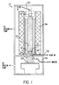
- FIGURE 1 is a schematic, sectioned, front view of a typical arc jet deposition apparatus known in the art which has been modified by the addition of water injection means for practicing the present method.
- FIGURE 2 is a schematic, cross-sectional view of a solid state particle detector device made with the diamond material of the present invention.
- FIG. 1 shows an arc jet apparatus 10.
- the apparatus 10 includes a cathode member 12 at the top end of a hollow barrel 14 in a metal jacket member 18 having an annular space 19 suitable for holding a fluid coolant.
- the barrel 14 and jacket member 18 are surrounded by a fluid-cooled magnetic coil assembly 20.
- an anode member 22 Longitudinally spaced at the end of the barrel 14 opposite that of the cathode 12 is an anode member 22 having a central opening aligned with the axis of the barrel 14 and leading through a nozzle 24 into an evacuated deposition chamber 26 which has a cooled deposition substrate 28 spaced from the end of the nozzle 24.
- a gas injection means 30 is located to inject gas into the barrel 14.
- Other gas injection means 32 are located in the vicinity of the anode 22.
- hydrogen gas is injected through the injector tubes 30 and 32 at a predetermined rate. More hydrogen gas, mixed with methane, is injected through the tube 32. The concentration of methane is based on the total percentage of methane injected as a volume percent of the total gas injected through both tubes 30,32.
- a direct current arc is struck between the cathode 12 and anode 22.
- the enthalpy of the gas in the barrel is adjusted by control of the arc power to result in the desired temperature of the substrate 28, which is heated by the gas impinging from the nozzle 24. At this enthalpy, the hydrogen becomes partially dissociated hydrogen atoms.
- the magnetic coil assembly 20 around the barrel 14 generates a solenoidal magnetic field which has the effect of swirling the arc about the anode 22 to reduce anode erosion.
- the activated gas mixture traveling through the nozzle 24 enters the evacuated deposition chamber 26 and impinges on a fluid-cooled deposition substrate 28 therein to form a diamond film on it.
- the methane enters the activated gas through the tubes 32, it too becomes partially dissociated into unstable hydrocarbon radical species.
- a set of three aluminum oxide ceramic tubules 34 positioned in radial symmetry with their ends in the deposition zone between the nozzle 24 and the substrate 28 are fed with water by a peristaltic pump, not shown.
- the hydrogen acts as a facilitating gas for the deposition of the carbon atoms from the activated hydrocarbon radicals as diamond crystallites bonded to each other.
- the diamond crystallites consist of carbon atoms bonded chemically to each other by What is generally referred to as "sp3" bonds.
- Apparatus of the arc jet type such as the apparatus 10 described above, is known in the art, except for the water injection apparatus including the tubules 34.
- the water injection apparatus including the tubules 34.
- the most important ones are generally the enthalpy (kilojoules/gram), vacuum level (torr), substrate temperature (degrees Celsius), methane concentration (percent), and water injection rate.
- the others can be determined for a given apparatus design and method of operation by the skilled operators familiar therewith without the necessity of undue experimentation.
- Such parameters do not lend themselves well to generalization, since they are dependent on specific apparatus design features.
- the deposition substrate is preferably molybdenum which has been coated with a thin layer about 3 microns (micro-meters) thick of titanium nitride, such as by vapor deposition, to reduce the adherence of the diamond to the substrate for better release of the film.
- Diamond film samples were made on an apparatus essentially similar to the jet apparatus 10 described above. In each case, the arc power was between 20 and 40 kilowatts and the deposition rate was between 3 and 6 microns per hour. The temperature of the substrate is in degrees C (Celsius). deposition conditions Sample A B C D E F chamber press. (torr) 12 12 12 12 12 12 substrate temp. (C) 825 844 825 933 850 840 % methane .050 .052 .076 .050 .072 .050 enthalpy (kJ/g) 32.9 31.8 35.4 34.5 50.4 35.3 power in kW 29.6 28.6 31.8 31.2 31.6 31.8 water in g/min.
- the substrate temperature is in degrees Celsius as measured by a pyrometer.
- the percent methane is the proportion by volume of the methane in the gas added through the tubes 30,32.
- the enthalpy is in kilojoules per gram.
- the power is the arc power in kilowatts.
- the water injection rate is in grams per minute.
- the O/C molar ratio is the molar ratio of oxygen to carbon in the deposition zone between the nozzle 24 and the substrate 28.
- the thickness is that of the diamond being deposited on the substrate 28.
- the Raman FWHM is in units of reciprocal centimeters and is the full width at half the maximum of the Raman scattering 1332/cm peak which is characteristic of diamond.
- the thermal conductivity was measured by the converging wave method.
- the collection distances were measured with an electric field strength of 10 kilovolts per centimeter.
- the diamond material In order for the diamond material to have a long carrier collection distance, it is essential that it be substantially free from most crystal lattice defects. Since the defects are microscopic, it is useful to assess their concentration by measuring certain characteristics of diamond which have been found to provide some indication of the degree to which defects are present. These characteristics are Raman line width and the thermal conductivity.
- the Raman linewidth is the full line-width at half the maximum of the 1332/cm frequency Raman scattering spectrum line of diamond. This width gives an indication of the degree of ordering of the diamond.
- the analysis of the samples A-F show that diamond with larger Raman line widths has much reduced collection distances.
- the examples show that a narrow Raman line profile, while perhaps not alone a sufficient condition for determining that a material will exhibit a long collection distance, does appear to be associated with material having a long collection distance.
- the diamond material in accordance with the present invention typically has a collection distance of 35-50 microns.
- the mobility is 3000-4000 cm2 V ⁇ 1 s ⁇ 1 and the lifetime is over 1 ns. This increased lifetime is much higher than that previously reported as best in the literature for CVD diamond (150 ps) and is even higher than for natural IIa diamond (300-550 ps).
- the addition of water is seen to greatly improve the lifetime. Under identical conditions except for water, the diamond made without water had a lifetime of 120 ps while the diamond made with water had a lifetime of over 1 ns. Both had mobilities of 3000-4000 cm2 V ⁇ 1 s ⁇ 1.
- the collection distance is measured by applying a voltage to the electrodes on each side of the diamond and analyzing the signal after it has been amplified by a charge-sensitive preamplifier and by a signal shaping amplifier.
- the initial particles to be detected can be from a radioactive source (e.g. strontium 90) or from a particle accelerator beam line.
- the collection distance is determined from where "Q gen " is the amount of charge generated by the ionizing radiation.
- Q meas " is the measured charge and "t” is the diamond thickness.
- Q gen is calculated by normalizing the diamond pulse height to the silicon pulse height (with corrections) or using a Monte Carlo simulation.
- the mobility and lifetime are measured by UV transient photoconductivity.
- One mm wide electrodes are deposited on the same side of the diamond with a 1 mm gap between the electrodes.
- the gap is illuminated with 3 to 5 ps (picosecond) pulses from a 202 nm frequency-multiplied Nd-YAG (neodymium-yttrium aluminum garnet) laser. These pulses are typically up to 20 ⁇ J/pulse at 10 Hz.
- the UV pulse creates electron-hole pairs and the subsequent current pulse is related to the carrier lifetime while the amplitude and total charge are related to the product of mobility and lifetime. In this test, only the top 2 microns at the surface is sampled due to the intrinsic absorption of UV light by diamond.
- the particle-induced conductivity tests the performance of the entire diamond thickness is sampled. Since the material on the substrate side is poorer and has small grain size, the particle-induced conductivity test gives a collection distance which is smaller than that deduced from the photoconductivity tests. The difference is typically a factor of two.
- FIGURE 2 of the drawings shows a particle detector 36 which features a wafer 38 of CVD diamond according to the present invention provided with two ohmic contact metal electrodes 40,42 on its faces.
- the electrodes 40,42 are connected to signal processing circuitry which includes a voltage source in series with a load resistor 46.
- An amplifier 48 is connected to the electrode 40 via an isolation capacitor 50.
- Electrodes could alternatively be in the form of interleaved comb-like structures which are both on the same face of the wafer. Such device structures are presently known in the art for use with diamond other than that of the present invention. The operation of the device is as described earlier in the discussion of such detector devices.
- oxidant such as carbon dioxide
- acetone, acetylene, and alcohols have been reported as substitutes for methane as the carbon source gas which would also contribute oxygen to the mix.
- concentrations are adjusted appropriately: generally each atom of oxygen bonds firmly to one carbon atom, so that a molecule such as acetone (CH3COCH3) contributes about as much free carbonaceous species as two molecules of methane (CH4).
- oxidant herein is used to denote substances traditionally considered in this class in the chemical arts.
- Tightly bonded molecules such as acetylene are less effective in producing diamond than are molecules like methane. However, if the residence time of the acetylene molecule is long enough, it may convert partially to more active species such as methane in flight. If the acetylene (or any other molecule) is injected into the arc, then it is substantially broken up and should count as if the carbon were present as methane (unless oxygen is present). Thus, it would be expected that one could obtain results similar to those described above in accordance with the invention by the use of carbon source gas other than methane which includes one or more oxygen atoms and is present in a concentration equivalent to that of the methane concentration disclosed herein in terms of the resulting active species.
- the invention is not intended to be limited to the use of methane alone as the carbon source gas or water alone as the oxidant source.
- water is a particularly advantageous oxidant source from the standpoint of convenience, cost, and safety considerations.
- the facilitating gas is hydrogen
Landscapes
- Chemical & Material Sciences (AREA)
- Engineering & Computer Science (AREA)
- Organic Chemistry (AREA)
- Physics & Mathematics (AREA)
- Inorganic Chemistry (AREA)
- General Chemical & Material Sciences (AREA)
- Chemical Kinetics & Catalysis (AREA)
- Materials Engineering (AREA)
- Mechanical Engineering (AREA)
- Metallurgy (AREA)
- Health & Medical Sciences (AREA)
- Plasma & Fusion (AREA)
- Life Sciences & Earth Sciences (AREA)
- General Physics & Mathematics (AREA)
- High Energy & Nuclear Physics (AREA)
- Molecular Biology (AREA)
- Spectroscopy & Molecular Physics (AREA)
- Crystals, And After-Treatments Of Crystals (AREA)
- Carbon And Carbon Compounds (AREA)
- Measurement Of Radiation (AREA)
Applications Claiming Priority (2)
| Application Number | Priority Date | Filing Date | Title |
|---|---|---|---|
| US9482693A | 1993-07-20 | 1993-07-20 | |
| US94826 | 1993-07-20 |
Publications (2)
| Publication Number | Publication Date |
|---|---|
| EP0635584A1 true EP0635584A1 (fr) | 1995-01-25 |
| EP0635584B1 EP0635584B1 (fr) | 1999-09-15 |
Family
ID=22247415
Family Applications (1)
| Application Number | Title | Priority Date | Filing Date |
|---|---|---|---|
| EP94202040A Revoked EP0635584B1 (fr) | 1993-07-20 | 1994-07-14 | Détecteur de rayonnement fabriqué en diamant CVD |
Country Status (5)
| Country | Link |
|---|---|
| US (2) | US5773830A (fr) |
| EP (1) | EP0635584B1 (fr) |
| JP (1) | JPH0782081A (fr) |
| CA (2) | CA2127832C (fr) |
| DE (1) | DE69420638T2 (fr) |
Cited By (6)
| Publication number | Priority date | Publication date | Assignee | Title |
|---|---|---|---|---|
| GB2358409A (en) * | 2000-01-06 | 2001-07-25 | Saint Gobain Ceramics | Thin film diamond coating and applications therefore |
| WO2001096633A1 (fr) * | 2000-06-15 | 2001-12-20 | Element Six (Pty) Ltd | Diamant monocristallin prepare par depot chimique en phase vapeur (cvd) |
| US6858080B2 (en) | 1998-05-15 | 2005-02-22 | Apollo Diamond, Inc. | Tunable CVD diamond structures |
| US7201886B2 (en) | 1998-05-15 | 2007-04-10 | Apollo Diamond, Inc. | Single crystal diamond tool |
| US7662441B2 (en) | 2003-01-10 | 2010-02-16 | Centre National De La Recherche Scientifique - Cnrs | High-speed diamond growth using a microwave plasma in pulsed mode |
| US8591856B2 (en) | 1998-05-15 | 2013-11-26 | SCIO Diamond Technology Corporation | Single crystal diamond electrochemical electrode |
Families Citing this family (12)
| Publication number | Priority date | Publication date | Assignee | Title |
|---|---|---|---|---|
| GB9812341D0 (en) * | 1998-06-08 | 1998-08-05 | De Beers Ind Diamond | Detector for ionising radiation |
| US6499426B1 (en) | 1999-12-10 | 2002-12-31 | Saint-Gobain Industrial Ceramics, Inc. | System and method for coating non-planar surfaces of objects with diamond film |
| DE60115435T2 (de) * | 2000-06-15 | 2006-08-31 | Element Six (Pty) Ltd. | Dicke einkristalline diamantschicht, verfahren zur herstellung der schicht und edelsteine hergestellt durch bearbeitung der schicht |
| AU2003205666A1 (en) * | 2002-01-25 | 2003-09-02 | Gesellschaft Fur Schwerionenforschung Mbh | Detector for detecting particle beams and method for the production thereof |
| GB0220767D0 (en) * | 2002-09-06 | 2002-10-16 | Diamanx Products Ltd | Diamond radiation detector |
| US7224532B2 (en) * | 2002-12-06 | 2007-05-29 | Chevron U.S.A. Inc. | Optical uses diamondoid-containing materials |
| US20050019955A1 (en) * | 2003-07-23 | 2005-01-27 | Dahl Jeremy E. | Luminescent heterodiamondoids as biological labels |
| KR100569417B1 (ko) * | 2004-08-13 | 2006-04-07 | 현대자동차주식회사 | 마이크로웨이브를 이용한 폐고무분말의 연속식표면개질장치와 이를 이용한 표면개질방법 |
| GB0813490D0 (en) * | 2008-07-23 | 2008-08-27 | Element Six Ltd | Solid state material |
| GB0813491D0 (en) | 2008-07-23 | 2008-08-27 | Element Six Ltd | Diamond Material |
| US9529098B2 (en) | 2013-09-30 | 2016-12-27 | Uchicago Argonne, Llc | X-ray monitoring optical elements |
| US10954607B1 (en) | 2019-10-22 | 2021-03-23 | Euclid Techlabs, Llc | High-efficiency transmission-mode diamond scintillator for quantitative characterization of X-ray beams |
Citations (2)
| Publication number | Priority date | Publication date | Assignee | Title |
|---|---|---|---|---|
| EP0286306A1 (fr) * | 1987-04-03 | 1988-10-12 | Fujitsu Limited | Méthode et appareil de déposition en phase gazeuse de diamant |
| EP0371145A1 (fr) * | 1988-05-28 | 1990-06-06 | Sumitomo Electric Industries, Ltd. | Procede de synthese en phase gazeuse de diamants |
Family Cites Families (14)
| Publication number | Priority date | Publication date | Assignee | Title |
|---|---|---|---|---|
| NL8006321A (nl) * | 1980-11-19 | 1982-06-16 | Eduard Anton Burgemeister | Werkwijze en inrichting voor het detecteren van ioniserende straling. |
| IL81537A (en) * | 1986-02-24 | 1991-05-12 | De Beers Ind Diamond | Method and synthetic diamond detector for detection of nuclear radiation |
| ZA874362B (en) * | 1986-06-20 | 1988-02-24 | De Beers Ind Diamond | Forming contacts on diamonds |
| EP0384084B1 (fr) * | 1988-12-28 | 1993-06-16 | De Beers Industrial Diamond Division (Proprietary) Limited | Détecteur de scintillations à diamant |
| JPH0794360B2 (ja) * | 1989-01-24 | 1995-10-11 | 住友電気工業株式会社 | ダイヤモンドの気相合成法 |
| US5079425A (en) * | 1990-01-10 | 1992-01-07 | Sumitomo Electric Industries, Ltd. | Radiation detecting element |
| US5209812A (en) * | 1990-04-09 | 1993-05-11 | Ford Motor Company | Hot filament method for growing high purity diamond |
| KR0184849B1 (ko) * | 1990-07-18 | 1999-05-01 | 하지메 히토추야나기 | 다이아몬드 제조방법 및 장치 |
| GB9018138D0 (en) * | 1990-08-17 | 1990-10-03 | De Beers Ind Diamond | Diamond alpha particle detector |
| GB9021689D0 (en) * | 1990-10-05 | 1990-11-21 | De Beers Ind Diamond | Diamond neutron detector |
| CA2122995A1 (fr) * | 1991-11-05 | 1993-05-13 | Ronald A. Rudder | Deposition chimique en phase vapeur de pellicules de diamant par des decharges de plasma a base d'eau |
| EP0582397A3 (fr) * | 1992-08-05 | 1995-01-25 | Crystallume | Matériel en diamant CVD pour détecteur de radiation et procédé pour fabriquer celui-ci. |
| CA2112308C (fr) * | 1993-01-22 | 2000-08-15 | Louis K. Bigelow | Methode de fabrication d'un film de diamant blanc |
| ZA946002B (en) * | 1993-08-12 | 1995-03-14 | De Beers Ind Diamond | Detecting ionising radiation |
-
1994
- 1994-07-12 CA CA002127832A patent/CA2127832C/fr not_active Expired - Fee Related
- 1994-07-12 CA CA002281972A patent/CA2281972C/fr not_active Expired - Fee Related
- 1994-07-14 DE DE69420638T patent/DE69420638T2/de not_active Expired - Fee Related
- 1994-07-14 EP EP94202040A patent/EP0635584B1/fr not_active Revoked
- 1994-07-20 JP JP6167915A patent/JPH0782081A/ja not_active Withdrawn
-
1995
- 1995-05-23 US US08/447,390 patent/US5773830A/en not_active Expired - Fee Related
- 1995-05-23 US US08/447,779 patent/US5672430A/en not_active Expired - Lifetime
Patent Citations (2)
| Publication number | Priority date | Publication date | Assignee | Title |
|---|---|---|---|---|
| EP0286306A1 (fr) * | 1987-04-03 | 1988-10-12 | Fujitsu Limited | Méthode et appareil de déposition en phase gazeuse de diamant |
| EP0371145A1 (fr) * | 1988-05-28 | 1990-06-06 | Sumitomo Electric Industries, Ltd. | Procede de synthese en phase gazeuse de diamants |
Non-Patent Citations (3)
| Title |
|---|
| MITSUDA ET AL.: "The growth of diamond in microwave plasma under low pressure", JOURNAL OF MATERIALS SCIENCE, vol. 22, 1987, LONDON GB, pages 1557 - 1562 * |
| PAN L S ET AL: "Particle- and photoinduced conductivity in type-IIa diamonds", JOURNAL OF APPLIED PHYSICS, 15 JULY 1993, USA, VOL. 74, NR. 2, PAGE(S) 1086 - 1095, ISSN 0021-8979 * |
| PLANO M A ET AL: "Polycrystalline CVD diamond films with high electrical mobility", SCIENCE, 28 MAY 1993, USA, VOL. 260, NR. 5112, PAGE(S) 1310 - 1312, ISSN 0036-8075 * |
Cited By (21)
| Publication number | Priority date | Publication date | Assignee | Title |
|---|---|---|---|---|
| US7459024B2 (en) | 1998-05-15 | 2008-12-02 | Apollo Diamond, Inc. | Method of forming an N-type doped single crystal diamond |
| US8591856B2 (en) | 1998-05-15 | 2013-11-26 | SCIO Diamond Technology Corporation | Single crystal diamond electrochemical electrode |
| US8187380B2 (en) | 1998-05-15 | 2012-05-29 | Apollo Diamond, Inc | Method of growing single crystal diamond in a plasma reactor |
| US7942966B2 (en) | 1998-05-15 | 2011-05-17 | Apollo Diamond, Inc. | Method of growing boron doped single crystal diamond in a plasma reactor |
| US6858080B2 (en) | 1998-05-15 | 2005-02-22 | Apollo Diamond, Inc. | Tunable CVD diamond structures |
| US7201886B2 (en) | 1998-05-15 | 2007-04-10 | Apollo Diamond, Inc. | Single crystal diamond tool |
| US7258741B2 (en) | 1998-05-15 | 2007-08-21 | Apollo Diamond, Inc. | System and method for producing synthetic diamond |
| US7560086B2 (en) | 1998-05-15 | 2009-07-14 | Apollo Diamond, Inc. | Single crystal diamond having 12C, 13C, and phosphorous |
| GB2358409B (en) * | 2000-01-06 | 2002-03-20 | Saint Gobain Ceramics | Corrosion and erosion resistant thin film diamond coating and applications therefor |
| US6605352B1 (en) | 2000-01-06 | 2003-08-12 | Saint-Gobain Ceramics & Plastics, Inc. | Corrosion and erosion resistant thin film diamond coating and applications therefor |
| GB2358409A (en) * | 2000-01-06 | 2001-07-25 | Saint Gobain Ceramics | Thin film diamond coating and applications therefore |
| GB2383588B (en) * | 2000-06-15 | 2004-05-05 | Element Six | Single crystal diamond prepared by CVD |
| EP1983080A2 (fr) | 2000-06-15 | 2008-10-22 | Element Six (PTY) Ltd | Diamant monocristallin préparé par CVD |
| KR100837033B1 (ko) * | 2000-06-15 | 2008-06-10 | 엘리먼트 씩스 (프티) 리미티드 | 화학 증착에 의해 제조된 단결정 다이아몬드 |
| AU2001274368B2 (en) * | 2000-06-15 | 2004-10-28 | Element Six (Pty) Ltd | Single crystal diamond prepared by cvd |
| GB2383588A (en) * | 2000-06-15 | 2003-07-02 | Element Six | Single crystal diamond prepared by CVD |
| EP1983080A3 (fr) * | 2000-06-15 | 2012-12-19 | Element Six (Pty) Ltd | Diamant monocristallin préparé par CVD |
| US8501143B2 (en) | 2000-06-15 | 2013-08-06 | Element Six Ltd. | Single crystal diamond prepared by CVD |
| WO2001096633A1 (fr) * | 2000-06-15 | 2001-12-20 | Element Six (Pty) Ltd | Diamant monocristallin prepare par depot chimique en phase vapeur (cvd) |
| US9103050B2 (en) | 2000-06-15 | 2015-08-11 | Element Six Technologies Limited | Single crystal diamond prepared by CVD |
| US7662441B2 (en) | 2003-01-10 | 2010-02-16 | Centre National De La Recherche Scientifique - Cnrs | High-speed diamond growth using a microwave plasma in pulsed mode |
Also Published As
| Publication number | Publication date |
|---|---|
| US5773830A (en) | 1998-06-30 |
| CA2281972A1 (fr) | 1995-01-21 |
| US5672430A (en) | 1997-09-30 |
| DE69420638T2 (de) | 2000-02-17 |
| EP0635584B1 (fr) | 1999-09-15 |
| JPH0782081A (ja) | 1995-03-28 |
| DE69420638D1 (de) | 1999-10-21 |
| CA2127832C (fr) | 2001-02-20 |
| CA2127832A1 (fr) | 1995-01-21 |
| CA2281972C (fr) | 2000-10-17 |
Similar Documents
| Publication | Publication Date | Title |
|---|---|---|
| EP0635584B1 (fr) | Détecteur de rayonnement fabriqué en diamant CVD | |
| US8501143B2 (en) | Single crystal diamond prepared by CVD | |
| Pryor | Carbon‐doped boron nitride cold cathodes | |
| EP0381111B1 (fr) | Couche de passivation électroactive | |
| Klein et al. | Photodetachment threshold of CN− by laser optogalvanic spectroscopy | |
| Tochitani et al. | Deposition of silicon oxide films from TEOS by low frequency plasma chemical vapor deposition | |
| Arnal et al. | Plasma etching in magnetic multipole microwave discharge | |
| Szekeres et al. | The effect of O2 plasma on properties of the Si SiO2 system | |
| Foulon et al. | CVD diamond films for radiation detection | |
| Dutton et al. | Ionization coefficients in helium, neon and helium-neon mixtures | |
| Ellis et al. | Secondary‐Electron Energy Distribution Studies of UO2 Surfaces | |
| Eryu et al. | Formation of an ohmic electrode in SiC using a pulsed laser irradiation method | |
| Bommakanti et al. | Time‐resolved prebreakdown x‐ray emission from polycrystalline alumina‐bridged vacuum gaps for impulse stresses | |
| Ismail et al. | Pressure dependence of the electrical potential and electron temperature in a microwave-generated plasma | |
| Ujihara et al. | Triggering of spark gaps by laser-induced ion emission | |
| Selwyn et al. | Plasma‐enhanced photoemission in argon discharges: Signal characterization and silicon doping effects | |
| Gan et al. | Effect of X-ray irradiation on the properties of alumina ceramics | |
| Asokan et al. | Pre-flashover luminosity along an alumina/vacuum interface | |
| Powell | Vacuum‐ultraviolet‐induced space charge in Al2O3 films | |
| Pinčı́k et al. | Properties of semiconductor surfaces covered with very thin insulating overlayers prepared by impacts of low-energy particles | |
| Paracchini | Electron impact processes in CdF2: Gd crystals | |
| Godet et al. | Density of States of Amorphous Germanium Thin Films Deposited by the Pecvd of H2-Diluted Germane | |
| Tarasenko | Denis Grigoryev, Vadim Novikov, Dmitriy Bezrodnyy, Viktor | |
| Lal et al. | Effect of diamond film quality on tungsten related photoluminescence peaks | |
| Khan et al. | High field flashover strength of intrinsic gallium nitride and aluminum nitride in vacuum |
Legal Events
| Date | Code | Title | Description |
|---|---|---|---|
| PUAI | Public reference made under article 153(3) epc to a published international application that has entered the european phase |
Free format text: ORIGINAL CODE: 0009012 |
|
| AK | Designated contracting states |
Kind code of ref document: A1 Designated state(s): DE FR GB |
|
| 17P | Request for examination filed |
Effective date: 19950603 |
|
| 17Q | First examination report despatched |
Effective date: 19960613 |
|
| RAP1 | Party data changed (applicant data changed or rights of an application transferred) |
Owner name: SAINT-GOBAIN INDUSTRIAL CERAMICS, INC. |
|
| GRAG | Despatch of communication of intention to grant |
Free format text: ORIGINAL CODE: EPIDOS AGRA |
|
| GRAG | Despatch of communication of intention to grant |
Free format text: ORIGINAL CODE: EPIDOS AGRA |
|
| GRAH | Despatch of communication of intention to grant a patent |
Free format text: ORIGINAL CODE: EPIDOS IGRA |
|
| GRAH | Despatch of communication of intention to grant a patent |
Free format text: ORIGINAL CODE: EPIDOS IGRA |
|
| GRAA | (expected) grant |
Free format text: ORIGINAL CODE: 0009210 |
|
| AK | Designated contracting states |
Kind code of ref document: B1 Designated state(s): DE FR GB |
|
| REF | Corresponds to: |
Ref document number: 69420638 Country of ref document: DE Date of ref document: 19991021 |
|
| ET | Fr: translation filed | ||
| PLBQ | Unpublished change to opponent data |
Free format text: ORIGINAL CODE: EPIDOS OPPO |
|
| PLBI | Opposition filed |
Free format text: ORIGINAL CODE: 0009260 |
|
| PLBF | Reply of patent proprietor to notice(s) of opposition |
Free format text: ORIGINAL CODE: EPIDOS OBSO |
|
| 26 | Opposition filed |
Opponent name: DIAMANX PRODUCTS LIMITED I.O.M. FREEPORT Effective date: 20000615 |
|
| PLBF | Reply of patent proprietor to notice(s) of opposition |
Free format text: ORIGINAL CODE: EPIDOS OBSO |
|
| PLBF | Reply of patent proprietor to notice(s) of opposition |
Free format text: ORIGINAL CODE: EPIDOS OBSO |
|
| REG | Reference to a national code |
Ref country code: GB Ref legal event code: IF02 |
|
| PGFP | Annual fee paid to national office [announced via postgrant information from national office to epo] |
Ref country code: GB Payment date: 20040707 Year of fee payment: 11 |
|
| PGFP | Annual fee paid to national office [announced via postgrant information from national office to epo] |
Ref country code: FR Payment date: 20040720 Year of fee payment: 11 |
|
| PGFP | Annual fee paid to national office [announced via postgrant information from national office to epo] |
Ref country code: DE Payment date: 20040831 Year of fee payment: 11 |
|
| PLAB | Opposition data, opponent's data or that of the opponent's representative modified |
Free format text: ORIGINAL CODE: 0009299OPPO |
|
| PLAQ | Examination of admissibility of opposition: information related to despatch of communication + time limit deleted |
Free format text: ORIGINAL CODE: EPIDOSDOPE2 |
|
| PLAR | Examination of admissibility of opposition: information related to receipt of reply deleted |
Free format text: ORIGINAL CODE: EPIDOSDOPE4 |
|
| PLBQ | Unpublished change to opponent data |
Free format text: ORIGINAL CODE: EPIDOS OPPO |
|
| R26 | Opposition filed (corrected) |
Opponent name: DIAMANX PRODUCTS LIMITED Effective date: 20000615 |
|
| PG25 | Lapsed in a contracting state [announced via postgrant information from national office to epo] |
Ref country code: GB Free format text: LAPSE BECAUSE OF NON-PAYMENT OF DUE FEES Effective date: 20050714 |
|
| RDAF | Communication despatched that patent is revoked |
Free format text: ORIGINAL CODE: EPIDOSNREV1 |
|
| RDAG | Patent revoked |
Free format text: ORIGINAL CODE: 0009271 |
|
| STAA | Information on the status of an ep patent application or granted ep patent |
Free format text: STATUS: PATENT REVOKED |
|
| GBPC | Gb: european patent ceased through non-payment of renewal fee |
Effective date: 20050714 |
|
| 27W | Patent revoked |
Effective date: 20051028 |
|
| PLAB | Opposition data, opponent's data or that of the opponent's representative modified |
Free format text: ORIGINAL CODE: 0009299OPPO |