EP0633542B1 - Dispositif électro-optique - Google Patents
Dispositif électro-optique Download PDFInfo
- Publication number
- EP0633542B1 EP0633542B1 EP94201882A EP94201882A EP0633542B1 EP 0633542 B1 EP0633542 B1 EP 0633542B1 EP 94201882 A EP94201882 A EP 94201882A EP 94201882 A EP94201882 A EP 94201882A EP 0633542 B1 EP0633542 B1 EP 0633542B1
- Authority
- EP
- European Patent Office
- Prior art keywords
- array
- elements
- photosensitive
- display
- row
- Prior art date
- Legal status (The legal status is an assumption and is not a legal conclusion. Google has not performed a legal analysis and makes no representation as to the accuracy of the status listed.)
- Expired - Lifetime
Links
Images

Classifications
-
- G—PHYSICS
- G06—COMPUTING; CALCULATING OR COUNTING
- G06F—ELECTRIC DIGITAL DATA PROCESSING
- G06F3/00—Input arrangements for transferring data to be processed into a form capable of being handled by the computer; Output arrangements for transferring data from processing unit to output unit, e.g. interface arrangements
- G06F3/01—Input arrangements or combined input and output arrangements for interaction between user and computer
- G06F3/03—Arrangements for converting the position or the displacement of a member into a coded form
- G06F3/041—Digitisers, e.g. for touch screens or touch pads, characterised by the transducing means
- G06F3/0412—Digitisers structurally integrated in a display
-
- G—PHYSICS
- G02—OPTICS
- G02F—OPTICAL DEVICES OR ARRANGEMENTS FOR THE CONTROL OF LIGHT BY MODIFICATION OF THE OPTICAL PROPERTIES OF THE MEDIA OF THE ELEMENTS INVOLVED THEREIN; NON-LINEAR OPTICS; FREQUENCY-CHANGING OF LIGHT; OPTICAL LOGIC ELEMENTS; OPTICAL ANALOGUE/DIGITAL CONVERTERS
- G02F1/00—Devices or arrangements for the control of the intensity, colour, phase, polarisation or direction of light arriving from an independent light source, e.g. switching, gating or modulating; Non-linear optics
- G02F1/01—Devices or arrangements for the control of the intensity, colour, phase, polarisation or direction of light arriving from an independent light source, e.g. switching, gating or modulating; Non-linear optics for the control of the intensity, phase, polarisation or colour
- G02F1/13—Devices or arrangements for the control of the intensity, colour, phase, polarisation or direction of light arriving from an independent light source, e.g. switching, gating or modulating; Non-linear optics for the control of the intensity, phase, polarisation or colour based on liquid crystals, e.g. single liquid crystal display cells
- G02F1/133—Constructional arrangements; Operation of liquid crystal cells; Circuit arrangements
- G02F1/1333—Constructional arrangements; Manufacturing methods
- G02F1/13338—Input devices, e.g. touch panels
-
- G—PHYSICS
- G09—EDUCATION; CRYPTOGRAPHY; DISPLAY; ADVERTISING; SEALS
- G09F—DISPLAYING; ADVERTISING; SIGNS; LABELS OR NAME-PLATES; SEALS
- G09F3/00—Labels, tag tickets, or similar identification or indication means; Seals; Postage or like stamps
-
- G—PHYSICS
- G09—EDUCATION; CRYPTOGRAPHY; DISPLAY; ADVERTISING; SEALS
- G09G—ARRANGEMENTS OR CIRCUITS FOR CONTROL OF INDICATING DEVICES USING STATIC MEANS TO PRESENT VARIABLE INFORMATION
- G09G3/00—Control arrangements or circuits, of interest only in connection with visual indicators other than cathode-ray tubes
-
- G—PHYSICS
- G09—EDUCATION; CRYPTOGRAPHY; DISPLAY; ADVERTISING; SEALS
- G09G—ARRANGEMENTS OR CIRCUITS FOR CONTROL OF INDICATING DEVICES USING STATIC MEANS TO PRESENT VARIABLE INFORMATION
- G09G2310/00—Command of the display device
- G09G2310/02—Addressing, scanning or driving the display screen or processing steps related thereto
- G09G2310/0264—Details of driving circuits
- G09G2310/0267—Details of drivers for scan electrodes, other than drivers for liquid crystal, plasma or OLED displays
-
- G—PHYSICS
- G09—EDUCATION; CRYPTOGRAPHY; DISPLAY; ADVERTISING; SEALS
- G09G—ARRANGEMENTS OR CIRCUITS FOR CONTROL OF INDICATING DEVICES USING STATIC MEANS TO PRESENT VARIABLE INFORMATION
- G09G2310/00—Command of the display device
- G09G2310/02—Addressing, scanning or driving the display screen or processing steps related thereto
- G09G2310/0264—Details of driving circuits
- G09G2310/0275—Details of drivers for data electrodes, other than drivers for liquid crystal, plasma or OLED displays, not related to handling digital grey scale data or to communication of data to the pixels by means of a current
Claims (15)
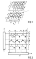
- Dispositif électro-optique comprenant un premier substrat (2) portant un affichage électro-optique (3) ayant un premier réseau (4) d'éléments d'affichage (5) et de conducteurs (12, 13) pour adresser des éléments d'affichage afin de permettre à l'affichage d'afficher une image, un deuxième substrat (6) portant un deuxième réseau (7) d'éléments (8) adressables par des conducteurs (9, 10) et des éléments photosensibles (11) associés aux conducteurs (9, 10) pour délivrer, lorsqu'ils sont éclairés, des signaux le long des conducteurs afin d'accéder aux éléments (8) du deuxième réseau (7), le deuxième substrat étant appliqué en regard du premier substrat (2) de telle sorte que les éléments photosensibles (11) soient associés à des éléments choisis (5') des éléments d'affichage (5) afin de permettre aux éléments d'affichage sélectionnés d'éclairer les éléments photosensibles, permettant ainsi de commander l'accès aux éléments du deuxième réseau par l'affichage.
- Dispositif électro-optique selon la revendication 1, dans lequel l'affichage électro-optique (3) comprend un réseau matriciel bidimensionnel d'éléments d'affichage (5) agencés en rangées et en colonnes avec des conducteurs de rangées et de colonnes associés (12, 13) et le deuxième réseau (7) est un réseau bidimensionnel d'éléments (8) agencés en rangées et en colonnes, les conducteurs de rangées et de colonnes (9, 10) étant associés aux éléments du deuxième réseau de telle sorte que l'acheminement de signaux à un conducteur de rangée choisi et à un conducteur de colonne choisi du deuxième réseau permette d'accéder à un élément du deuxième réseau et les conducteurs de rangées et de colonnes du deuxième réseau étant associés à des éléments photosensibles (11) pour acheminer, lorsqu'ils sont éclairés par certains, choisis, des éléments d'affichage, des signaux le long des conducteurs de rangées et de colonnes afin d'accéder aux éléments du deuxième réseau.
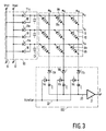
- Dispositif électro-optique selon la revendication 2, dans lequel chaque élément (8) du deuxième réseau (7) est agencé pour stocker une charge et chaque conducteur de rangée (9) du deuxième réseau est couplé à une ligne d'alimentation en tension de sélection (17) via au moins un élément photosensible respectif (11) de telle sorte que, lors du fonctionnement du dispositif électro-optique pour lire la charge stockée dans l'élément au sein d'une rangée, le au moins un élément photosensible associé à la rangée soit éclairé par l'affichage pour coupler la tension de sélection au conducteur de rangée.
- Dispositif électro-optique selon la revendication 3, dans lequel chaque conducteur de rangée (9) du deuxième réseau (7) est couplé à une ligne d'alimentation de tension de remise à zéro (19) via un élément de commutation respectif (18) pour permettre d'appliquer une impulsion de tension de remise à zéro au conducteur de rangée afin de remettre à zéro les éléments associés.
- Dispositif électro-optique selon la revendication 3 ou 4, dans lequel chaque conducteur de colonne (10) du deuxième réseau (7) est connecté par au moins un premier élément photosensible (11) à une électrode d'un condensateur de colonne respectif (C) dont l'autre électrode est couplée à un amplificateur sensible à la charge (21) et à au moins un deuxième élément photosensible (11) qui est couplé à une ligne de référence de tension (22) de telle sorte que, pour lire la charge dans un élément qui se trouve dans une colonne donnée du deuxième réseau, tout d'abord, le au moins un premier élément photosensible associé soit éclairé par l'affichage pour permettre à la charge stockée dans un élément dans à la fois la colonne et une rangée à laquelle la tension de sélection est appliquée d'être transférée via le conducteur de colonne et le au moins un premier élément photosensible au condensateur et qu'ensuite, le au moins un deuxième élément photosensible soit éclairé pour permettre de transférer la charge stockée dans le condensateur de colonne à l'amplificateur sensible à la charge.
- Dispositif électro-optique selon la revendication 3 ou 4, dans lequel chaque conducteur de colonne (10) est couplé à une électrode de chacun des premier et second condensateurs de colonnes (C, C') par des premiers éléments photosensibles respectifs (11b, 11b'), chaque condensateur ayant son autre électrode couplée à un amplificateur sensible à la charge respectif (21, 21') et à un deuxième élément photosensible respectif (11c, 11c') couplé à une ligne de référence de tension (22) de telle sorte que, pour lire la charge dans un élément à l'intérieur d'une colonne donnée du deuxième réseau, tout d'abord l'un des premiers éléments photosensibles associés soit éclairé par l'affichage pour permettre à la charge stockée dans un élément à la fois dans la colonne et une rangée à laquelle la tension de sélection est appliquée, d'être transférée via le conducteur de colonne et ledit un premier élément photosensible au condensateur associé du premier et du second condensateurs et qu'ensuite, le premier des deuxièmes éléments photosensibles soit éclairé pour permettre de transférer la charge stockée dans le condensateur de colonne à l'amplificateur sensible à la charge.
- Dispositif électro-optique selon l'une quelconque des revendications précédentes, dans lequel les éléments photosensibles (11) sont aménagés sur la périphérie du deuxième réseau (7).
- Dispositif électro-optique selon l'une quelconque des revendications précédentes, dans lequel chaque conducteur (9, 10) du deuxième réseau est associé à au moins un élément photosensible respectif (11).
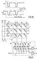
- Dispositif électro-optique selon l'une quelconque des revendications précédentes, dans lequel chaque conducteur (9, 10) du deuxième réseau (7) est associé à un certain nombre d'éléments photosensibles (11) aménagés de telle sorte que les signaux ne soient appliqués le long du conducteur que lorsque tous les éléments photosensibles associés sont éclairés.
- Dispositif électro-optique selon l'une quelconque des revendications précédentes, dans lequel les éléments photosensibles (11) associés à des conducteurs adjacents sont échelonnés de telle manière que l'espacement entre les éléments photosensibles associés à des conducteurs adjacents soit supérieur à l'espacement entre les conducteurs adjacents.
- Dispositif électro-optique selon l'une quelconque des revendications précédentes, dans lequel les premier et deuxième réseaux (4, 7) sont de taille comparable et les éléments d'affichage (5) destinés à éclairer les éléments photosensibles sont aménagés sur la périphérie du premier réseau.
- Dispositif électro-optique selon l'une quelconque des revendications précédentes, dans lequel l'affichage comprend un affichage à cristaux liquides.
- Dispositif électro-optique selon l'une quelconque des revendications précédentes, dans lequel le deuxième réseau (7) comprend un réseau d'autres éléments photosensibles (8a).
- Dispositif électro-optique selon l'une quelconque des revendications précédentes, dans lequel le deuxième substrat (6) portant le deuxième réseau (7) est monté sur le premier substrat (2) portant le premier réseau (4).
- Dispositif électro-optique selon l'une quelconque des revendications précédentes, dans lequel le deuxième substrat (6) portant le deuxième réseau est séparable du premier substrat portant le premier réseau.
Applications Claiming Priority (2)
| Application Number | Priority Date | Filing Date | Title |
|---|---|---|---|
| GB9313841 | 1993-07-05 | ||
| GB939313841A GB9313841D0 (en) | 1993-07-05 | 1993-07-05 | An electro-optic device |
Publications (3)
| Publication Number | Publication Date |
|---|---|
| EP0633542A2 EP0633542A2 (fr) | 1995-01-11 |
| EP0633542A3 EP0633542A3 (fr) | 1998-06-10 |
| EP0633542B1 true EP0633542B1 (fr) | 2001-10-17 |
Family
ID=10738301
Family Applications (1)
| Application Number | Title | Priority Date | Filing Date |
|---|---|---|---|
| EP94201882A Expired - Lifetime EP0633542B1 (fr) | 1993-07-05 | 1994-06-30 | Dispositif électro-optique |
Country Status (7)
| Country | Link |
|---|---|
| US (1) | US5483263A (fr) |
| EP (1) | EP0633542B1 (fr) |
| JP (1) | JPH0777704A (fr) |
| KR (1) | KR100350001B1 (fr) |
| DE (1) | DE69428638T2 (fr) |
| GB (1) | GB9313841D0 (fr) |
| TW (1) | TW250590B (fr) |
Cited By (17)
| Publication number | Priority date | Publication date | Assignee | Title |
|---|---|---|---|---|
| US7542178B2 (en) | 2003-01-21 | 2009-06-02 | Hewlett-Packard Development Company, L.P. | Electronic device display and document scanner |
| US7773139B2 (en) | 2004-04-16 | 2010-08-10 | Apple Inc. | Image sensor with photosensitive thin film transistors |
| US7830461B2 (en) | 2002-05-23 | 2010-11-09 | Apple Inc. | Light sensitive display |
| US7872641B2 (en) | 2002-02-20 | 2011-01-18 | Apple Inc. | Light sensitive display |
| US8207946B2 (en) | 2003-02-20 | 2012-06-26 | Apple Inc. | Light sensitive display |
| US8441422B2 (en) | 2002-02-20 | 2013-05-14 | Apple Inc. | Light sensitive display with object detection calibration |
| US8638320B2 (en) | 2011-06-22 | 2014-01-28 | Apple Inc. | Stylus orientation detection |
| US8928635B2 (en) | 2011-06-22 | 2015-01-06 | Apple Inc. | Active stylus |
| US9176604B2 (en) | 2012-07-27 | 2015-11-03 | Apple Inc. | Stylus device |
| US9310923B2 (en) | 2010-12-03 | 2016-04-12 | Apple Inc. | Input device for touch sensitive devices |
| US9329703B2 (en) | 2011-06-22 | 2016-05-03 | Apple Inc. | Intelligent stylus |
| US9557845B2 (en) | 2012-07-27 | 2017-01-31 | Apple Inc. | Input device for and method of communication with capacitive devices through frequency variation |
| US9652090B2 (en) | 2012-07-27 | 2017-05-16 | Apple Inc. | Device for digital communication through capacitive coupling |
| US9939935B2 (en) | 2013-07-31 | 2018-04-10 | Apple Inc. | Scan engine for touch controller architecture |
| US10048775B2 (en) | 2013-03-14 | 2018-08-14 | Apple Inc. | Stylus detection and demodulation |
| US10061449B2 (en) | 2014-12-04 | 2018-08-28 | Apple Inc. | Coarse scan and targeted active mode scan for touch and stylus |
| US10474277B2 (en) | 2016-05-31 | 2019-11-12 | Apple Inc. | Position-based stylus communication |
Families Citing this family (46)
| Publication number | Priority date | Publication date | Assignee | Title |
|---|---|---|---|---|
| US5917464A (en) * | 1994-10-18 | 1999-06-29 | Xerox Corporation | Combination of 2-D detector array with display for image processing |
| SE504169C2 (sv) * | 1995-02-13 | 1996-11-25 | Sten Eric Lindquist | Display kombinerad med solcell och batteri |
| GB9512942D0 (en) * | 1995-06-24 | 1995-08-30 | Philips Electronics Uk Ltd | Electronic devices comprising an array |
| US5900767A (en) * | 1995-06-24 | 1999-05-04 | U.S. Philips Corporation | Electronic devices comprising an array |
| WO1997005597A1 (fr) * | 1995-07-31 | 1997-02-13 | Litton Systems Canada Limited | Ensemble de pixels a ecran plat incorporant des commutateurs photoconducteurs |
| TW368671B (en) * | 1995-08-30 | 1999-09-01 | Tektronix Inc | Sputter-resistant, low-work-function, conductive coatings for cathode electrodes in DC plasma addressing structure |
| GB9524483D0 (en) * | 1995-11-30 | 1996-01-31 | Philips Electronics Nv | Light sensing array device and apparatus incorporating such |
| GB9614480D0 (en) * | 1995-12-01 | 1996-09-04 | Philips Electronics Nv | Multiplexer circuit |
| GB9524560D0 (en) * | 1995-12-01 | 1996-01-31 | Philips Electronics Nv | Multiplexer circuit |
| GB9603052D0 (en) * | 1996-02-14 | 1996-04-10 | Philips Electronics Nv | Image sensor |
| DE19720925B4 (de) * | 1996-05-29 | 2004-08-26 | Nawotec Gmbh | Einrichtung zur Eingabe von Informationen mittels eines sich der Einrichtung nähernden Gegenstandes |
| GB9616265D0 (en) * | 1996-08-02 | 1996-09-11 | Philips Electronics Uk Ltd | Electron devices |
| TW403928B (en) * | 1996-08-16 | 2000-09-01 | Tektronix Inc | Sputter-resistant conductive coatings with enhanced emission of electrons for cathode electrodes in DC plasma addressing structure |
| JP2000193938A (ja) * | 1998-12-28 | 2000-07-14 | Fujitsu Ltd | 液晶表示装置の駆動方法 |
| US7119759B2 (en) * | 1999-05-03 | 2006-10-10 | E Ink Corporation | Machine-readable displays |
| US7071907B1 (en) * | 1999-05-07 | 2006-07-04 | Candescent Technologies Corporation | Display with active contrast enhancement |
| GB0014962D0 (en) * | 2000-06-20 | 2000-08-09 | Koninkl Philips Electronics Nv | Matrix array display devices with light sensing elements and associated storage capacitors |
| GB2381643A (en) * | 2001-10-31 | 2003-05-07 | Cambridge Display Tech Ltd | Display drivers |
| US7023503B2 (en) * | 2002-02-20 | 2006-04-04 | Planar Systems, Inc. | Image sensor with photosensitive thin film transistors |
| AU2003216481A1 (en) * | 2002-03-01 | 2003-09-16 | Planar Systems, Inc. | Reflection resistant touch screens |
| JP2003332560A (ja) * | 2002-05-13 | 2003-11-21 | Semiconductor Energy Lab Co Ltd | 半導体装置及びマイクロプロセッサ |
| JP4227770B2 (ja) * | 2002-07-10 | 2009-02-18 | シャープ株式会社 | 表示装置およびそれを備えた画像読み取り/表示システム |
| JP4094386B2 (ja) | 2002-09-02 | 2008-06-04 | 株式会社半導体エネルギー研究所 | 電子回路装置 |
| JP4373063B2 (ja) | 2002-09-02 | 2009-11-25 | 株式会社半導体エネルギー研究所 | 電子回路装置 |
| US20060034492A1 (en) * | 2002-10-30 | 2006-02-16 | Roy Siegel | Hand recognition system |
| US7219241B2 (en) * | 2002-11-30 | 2007-05-15 | Intel Corporation | Method for managing virtual and actual performance states of logical processors in a multithreaded processor using system management mode |
| AU2003283737A1 (en) * | 2002-12-30 | 2004-07-22 | Koninklijke Philips Electronics N.V. | Display device with capacitively connected pads |
| WO2004066410A1 (fr) * | 2003-01-17 | 2004-08-05 | Diode Solutions, Inc. | Afficheur utilisant une matiere organique |
| JP4574118B2 (ja) * | 2003-02-12 | 2010-11-04 | 株式会社半導体エネルギー研究所 | 半導体装置及びその作製方法 |
| US20080048995A1 (en) * | 2003-02-20 | 2008-02-28 | Planar Systems, Inc. | Light sensitive display |
| US8283679B2 (en) * | 2003-06-30 | 2012-10-09 | Semiconductor Energy Laboratory Co., Ltd. | Semiconductor device having light-emitting element and light-receiving element for transmitting among circuits formed over the plurality of substrates |
| US20050134749A1 (en) * | 2003-12-19 | 2005-06-23 | Adiel Abileah | Reflection resistant display |
| US8421715B2 (en) * | 2004-05-21 | 2013-04-16 | Semiconductor Energy Laboratory Co., Ltd. | Display device, driving method thereof and electronic appliance |
| US20070109239A1 (en) * | 2005-11-14 | 2007-05-17 | Den Boer Willem | Integrated light sensitive liquid crystal display |
| RU2445258C2 (ru) * | 2006-04-04 | 2012-03-20 | Калисолар Канада Инк. | Способ очистки кремния |
| US7525608B2 (en) * | 2006-08-14 | 2009-04-28 | Hannstar Display Corp. | Input display and fabrication method thereof |
| US7898042B2 (en) | 2006-11-07 | 2011-03-01 | Cbrite Inc. | Two-terminal switching devices and their methods of fabrication |
| US9741901B2 (en) | 2006-11-07 | 2017-08-22 | Cbrite Inc. | Two-terminal electronic devices and their methods of fabrication |
| CN101627476B (zh) * | 2006-11-07 | 2013-03-27 | 希百特股份有限公司 | 金属-绝缘体-金属(mim)装置及其制备方法 |
| US10824931B2 (en) * | 2012-08-30 | 2020-11-03 | Féinics Amatech Teoranta | Contactless smartcards with multiple coupling frames |
| US9122349B1 (en) * | 2014-03-19 | 2015-09-01 | Bidirectional Display Inc. | Image sensor panel and method for capturing graphical information using same |
| WO2015143011A1 (fr) * | 2014-03-19 | 2015-09-24 | Bidirectional Display Inc. | Panneau de capteur d'image, et procédé de capture d'informations graphiques l'utilisant |
| CN106201149B (zh) * | 2016-08-02 | 2019-07-09 | 厦门天马微电子有限公司 | 触控显示面板及装置 |
| JP6933142B2 (ja) * | 2016-11-01 | 2021-09-08 | 東レ株式会社 | タッチパネル、タッチパネルの製造方法 |
| US10162462B2 (en) * | 2017-05-01 | 2018-12-25 | Synaptics Incorporated | Integrating capacitive sensing with an optical sensor |
| US11276346B2 (en) * | 2019-01-21 | 2022-03-15 | Novatek Microelectronics Corp. | Simplified sensing circuit and sample and hold circuit for improving uniformity in OLED driver |
Family Cites Families (9)
| Publication number | Priority date | Publication date | Assignee | Title |
|---|---|---|---|---|
| FR2469805A1 (fr) * | 1979-11-09 | 1981-05-22 | Thomson Csf | Matrice de detection d'un rayonnement electromagnetique et intensificateur d'images radiologiques comportant une telle matrice |
| JPS5685792A (en) * | 1979-12-14 | 1981-07-13 | Citizen Watch Co Ltd | Liquid crystal display unit |
| DE3511353A1 (de) * | 1985-03-28 | 1986-10-09 | Siemens Ag | Anordnung zum eingeben und verarbeiten von zeichen und/oder grafischen mustern |
| FR2593343B1 (fr) * | 1986-01-20 | 1988-03-25 | Thomson Csf | Matrice d'elements photosensibles et son procede de fabrication, procede de lecture associe, et application de cette matrice a la prise de vue d'images |
| US4952031A (en) * | 1987-06-19 | 1990-08-28 | Victor Company Of Japan, Ltd. | Liquid crystal display device |
| FR2627924B1 (fr) * | 1988-02-26 | 1990-06-22 | Thomson Csf | Dispositif photosensible et detecteur d'images comportant un tel dispositif, notamment detecteur d'images a double energie |
| FR2629932B1 (fr) * | 1988-04-11 | 1991-01-25 | Thomson Csf | Lecteur de documents |
| JPH02188818A (ja) * | 1989-01-18 | 1990-07-24 | Hitachi Ltd | 手書き入出力装置並びにこの手書き入出力装置を用いた手書き入力システム |
| GB9026040D0 (en) * | 1990-11-30 | 1991-01-16 | Philips Electronic Associated | Addressable matrix device |
-
1993
- 1993-07-05 GB GB939313841A patent/GB9313841D0/en active Pending
-
1994
- 1994-04-08 TW TW083103086A patent/TW250590B/zh active
- 1994-05-11 US US08/241,317 patent/US5483263A/en not_active Expired - Fee Related
- 1994-06-30 EP EP94201882A patent/EP0633542B1/fr not_active Expired - Lifetime
- 1994-06-30 DE DE69428638T patent/DE69428638T2/de not_active Expired - Fee Related
- 1994-06-30 KR KR1019940015381A patent/KR100350001B1/ko not_active IP Right Cessation
- 1994-07-04 JP JP15219194A patent/JPH0777704A/ja not_active Abandoned
Cited By (36)
| Publication number | Priority date | Publication date | Assignee | Title |
|---|---|---|---|---|
| US9134851B2 (en) | 2002-02-20 | 2015-09-15 | Apple Inc. | Light sensitive display |
| US11073926B2 (en) | 2002-02-20 | 2021-07-27 | Apple Inc. | Light sensitive display |
| US9411470B2 (en) | 2002-02-20 | 2016-08-09 | Apple Inc. | Light sensitive display with multiple data set object detection |
| US8570449B2 (en) | 2002-02-20 | 2013-10-29 | Apple Inc. | Light sensitive display with pressure sensor |
| US7872641B2 (en) | 2002-02-20 | 2011-01-18 | Apple Inc. | Light sensitive display |
| US8441422B2 (en) | 2002-02-20 | 2013-05-14 | Apple Inc. | Light sensitive display with object detection calibration |
| US7880819B2 (en) | 2002-05-23 | 2011-02-01 | Apple Inc. | Light sensitive display |
| US8044930B2 (en) | 2002-05-23 | 2011-10-25 | Apple Inc. | Light sensitive display |
| US7880733B2 (en) | 2002-05-23 | 2011-02-01 | Apple Inc. | Light sensitive display |
| US7852417B2 (en) | 2002-05-23 | 2010-12-14 | Apple Inc. | Light sensitive display |
| US7830461B2 (en) | 2002-05-23 | 2010-11-09 | Apple Inc. | Light sensitive display |
| US9354735B2 (en) | 2002-05-23 | 2016-05-31 | Apple Inc. | Light sensitive display |
| US7542178B2 (en) | 2003-01-21 | 2009-06-02 | Hewlett-Packard Development Company, L.P. | Electronic device display and document scanner |
| US8207946B2 (en) | 2003-02-20 | 2012-06-26 | Apple Inc. | Light sensitive display |
| US8289429B2 (en) | 2004-04-16 | 2012-10-16 | Apple Inc. | Image sensor with photosensitive thin film transistors and dark current compensation |
| US7773139B2 (en) | 2004-04-16 | 2010-08-10 | Apple Inc. | Image sensor with photosensitive thin film transistors |
| US9310923B2 (en) | 2010-12-03 | 2016-04-12 | Apple Inc. | Input device for touch sensitive devices |
| US9329703B2 (en) | 2011-06-22 | 2016-05-03 | Apple Inc. | Intelligent stylus |
| US8928635B2 (en) | 2011-06-22 | 2015-01-06 | Apple Inc. | Active stylus |
| US8638320B2 (en) | 2011-06-22 | 2014-01-28 | Apple Inc. | Stylus orientation detection |
| US9519361B2 (en) | 2011-06-22 | 2016-12-13 | Apple Inc. | Active stylus |
| US9921684B2 (en) | 2011-06-22 | 2018-03-20 | Apple Inc. | Intelligent stylus |
| US9557845B2 (en) | 2012-07-27 | 2017-01-31 | Apple Inc. | Input device for and method of communication with capacitive devices through frequency variation |
| US9582105B2 (en) | 2012-07-27 | 2017-02-28 | Apple Inc. | Input device for touch sensitive devices |
| US9652090B2 (en) | 2012-07-27 | 2017-05-16 | Apple Inc. | Device for digital communication through capacitive coupling |
| US9176604B2 (en) | 2012-07-27 | 2015-11-03 | Apple Inc. | Stylus device |
| US10048775B2 (en) | 2013-03-14 | 2018-08-14 | Apple Inc. | Stylus detection and demodulation |
| US9939935B2 (en) | 2013-07-31 | 2018-04-10 | Apple Inc. | Scan engine for touch controller architecture |
| US10067580B2 (en) | 2013-07-31 | 2018-09-04 | Apple Inc. | Active stylus for use with touch controller architecture |
| US10845901B2 (en) | 2013-07-31 | 2020-11-24 | Apple Inc. | Touch controller architecture |
| US11687192B2 (en) | 2013-07-31 | 2023-06-27 | Apple Inc. | Touch controller architecture |
| US10061450B2 (en) | 2014-12-04 | 2018-08-28 | Apple Inc. | Coarse scan and targeted active mode scan for touch |
| US10067618B2 (en) | 2014-12-04 | 2018-09-04 | Apple Inc. | Coarse scan and targeted active mode scan for touch |
| US10664113B2 (en) | 2014-12-04 | 2020-05-26 | Apple Inc. | Coarse scan and targeted active mode scan for touch and stylus |
| US10061449B2 (en) | 2014-12-04 | 2018-08-28 | Apple Inc. | Coarse scan and targeted active mode scan for touch and stylus |
| US10474277B2 (en) | 2016-05-31 | 2019-11-12 | Apple Inc. | Position-based stylus communication |
Also Published As
| Publication number | Publication date |
|---|---|
| GB9313841D0 (en) | 1993-08-18 |
| DE69428638T2 (de) | 2002-07-04 |
| US5483263A (en) | 1996-01-09 |
| JPH0777704A (ja) | 1995-03-20 |
| KR100350001B1 (ko) | 2002-12-26 |
| KR950003856A (ko) | 1995-02-17 |
| TW250590B (fr) | 1995-07-01 |
| DE69428638D1 (de) | 2001-11-22 |
| EP0633542A2 (fr) | 1995-01-11 |
| EP0633542A3 (fr) | 1998-06-10 |
Similar Documents
| Publication | Publication Date | Title |
|---|---|---|
| EP0633542B1 (fr) | Dispositif électro-optique | |
| EP0569090B1 (fr) | Capteur d'image | |
| US5446564A (en) | Liquid crystal display device having photosensor at each pixel | |
| KR100470881B1 (ko) | 전기회로 | |
| EP0509589B1 (fr) | Dispositif d'entrée tactile optique | |
| JP2774424B2 (ja) | 画像入力一体型表示装置 | |
| EP0490683B1 (fr) | Matrices de capteurs | |
| JP4590340B2 (ja) | 液晶表示装置及び液晶表示装置を用いたイメージセンシング方法 | |
| US7477445B2 (en) | Electrophoretic indication display | |
| KR101345025B1 (ko) | 전기 광학 장치 및 전자 기기 | |
| US8508484B2 (en) | Liquid crystal display device | |
| KR101090254B1 (ko) | 감지 소자를 내장한 표시 장치 | |
| KR20070027051A (ko) | 접촉 감지 기능이 있는 표시 장치 | |
| US5838290A (en) | Display device with photovoltaic converter | |
| US5426292A (en) | Image sensor having a two dimensional array of imaging elements with opposite polarity leakage currents | |
| US6753839B2 (en) | Electro-optical panel and electronic device | |
| JPH0797190B2 (ja) | 記憶装置および液晶表示装置 | |
| WO2003071342A1 (fr) | Panneau d'affichage a cristaux liquides possedant une partie d'acquisition des images et procede de fabrication correspondant | |
| CN113946241A (zh) | 显示面板及显示终端 | |
| JP2006509231A (ja) | アクティブ・マトリックス表示装置 | |
| US11842007B1 (en) | Display panel and display device | |
| WO1997005597A1 (fr) | Ensemble de pixels a ecran plat incorporant des commutateurs photoconducteurs | |
| CN101086562A (zh) | 平面显示器数字像素结合微感测阵列 |
Legal Events
| Date | Code | Title | Description |
|---|---|---|---|
| PUAI | Public reference made under article 153(3) epc to a published international application that has entered the european phase |
Free format text: ORIGINAL CODE: 0009012 |
|
| AK | Designated contracting states |
Kind code of ref document: A2 Designated state(s): DE FR GB NL |
|
| PUAL | Search report despatched |
Free format text: ORIGINAL CODE: 0009013 |
|
| AK | Designated contracting states |
Kind code of ref document: A3 Designated state(s): DE FR GB NL |
|
| 17P | Request for examination filed |
Effective date: 19981210 |
|
| 17Q | First examination report despatched |
Effective date: 19990308 |
|
| GRAG | Despatch of communication of intention to grant |
Free format text: ORIGINAL CODE: EPIDOS AGRA |
|
| GRAG | Despatch of communication of intention to grant |
Free format text: ORIGINAL CODE: EPIDOS AGRA |
|
| GRAH | Despatch of communication of intention to grant a patent |
Free format text: ORIGINAL CODE: EPIDOS IGRA |
|
| GRAH | Despatch of communication of intention to grant a patent |
Free format text: ORIGINAL CODE: EPIDOS IGRA |
|
| GRAA | (expected) grant |
Free format text: ORIGINAL CODE: 0009210 |
|
| AK | Designated contracting states |
Kind code of ref document: B1 Designated state(s): DE FR GB NL |
|
| PG25 | Lapsed in a contracting state [announced via postgrant information from national office to epo] |
Ref country code: NL Free format text: LAPSE BECAUSE OF FAILURE TO SUBMIT A TRANSLATION OF THE DESCRIPTION OR TO PAY THE FEE WITHIN THE PRESCRIBED TIME-LIMIT Effective date: 20011017 |
|
| REF | Corresponds to: |
Ref document number: 69428638 Country of ref document: DE Date of ref document: 20011122 |
|
| REG | Reference to a national code |
Ref country code: GB Ref legal event code: IF02 |
|
| ET | Fr: translation filed | ||
| NLV1 | Nl: lapsed or annulled due to failure to fulfill the requirements of art. 29p and 29m of the patents act | ||
| PLBE | No opposition filed within time limit |
Free format text: ORIGINAL CODE: 0009261 |
|
| STAA | Information on the status of an ep patent application or granted ep patent |
Free format text: STATUS: NO OPPOSITION FILED WITHIN TIME LIMIT |
|
| 26N | No opposition filed | ||
| PGFP | Annual fee paid to national office [announced via postgrant information from national office to epo] |
Ref country code: FR Payment date: 20030625 Year of fee payment: 10 |
|
| PGFP | Annual fee paid to national office [announced via postgrant information from national office to epo] |
Ref country code: GB Payment date: 20030627 Year of fee payment: 10 |
|
| PGFP | Annual fee paid to national office [announced via postgrant information from national office to epo] |
Ref country code: DE Payment date: 20030818 Year of fee payment: 10 |
|
| PG25 | Lapsed in a contracting state [announced via postgrant information from national office to epo] |
Ref country code: GB Free format text: LAPSE BECAUSE OF NON-PAYMENT OF DUE FEES Effective date: 20040630 |
|
| PG25 | Lapsed in a contracting state [announced via postgrant information from national office to epo] |
Ref country code: DE Free format text: LAPSE BECAUSE OF NON-PAYMENT OF DUE FEES Effective date: 20050101 |
|
| GBPC | Gb: european patent ceased through non-payment of renewal fee |
Effective date: 20040630 |
|
| PG25 | Lapsed in a contracting state [announced via postgrant information from national office to epo] |
Ref country code: FR Free format text: LAPSE BECAUSE OF NON-PAYMENT OF DUE FEES Effective date: 20050228 |
|
| REG | Reference to a national code |
Ref country code: FR Ref legal event code: ST |