EP0627707B1 - Procédé de fabrication d'une carte à mémoire et carte à mémoire ainsi obtenue - Google Patents
Procédé de fabrication d'une carte à mémoire et carte à mémoire ainsi obtenue Download PDFInfo
- Publication number
- EP0627707B1 EP0627707B1 EP93401397A EP93401397A EP0627707B1 EP 0627707 B1 EP0627707 B1 EP 0627707B1 EP 93401397 A EP93401397 A EP 93401397A EP 93401397 A EP93401397 A EP 93401397A EP 0627707 B1 EP0627707 B1 EP 0627707B1
- Authority
- EP
- European Patent Office
- Prior art keywords
- integrated circuit
- cavity
- conductors
- terminals
- adhesive strip
- Prior art date
- Legal status (The legal status is an assumption and is not a legal conclusion. Google has not performed a legal analysis and makes no representation as to the accuracy of the status listed.)
- Expired - Lifetime
Links
Images


Classifications
-
- H—ELECTRICITY
- H10—SEMICONDUCTOR DEVICES; ELECTRIC SOLID-STATE DEVICES NOT OTHERWISE PROVIDED FOR
- H10W—GENERIC PACKAGES, INTERCONNECTIONS, CONNECTORS OR OTHER CONSTRUCTIONAL DETAILS OF DEVICES COVERED BY CLASS H10
- H10W70/00—Package substrates; Interposers; Redistribution layers [RDL]
- H10W70/01—Manufacture or treatment
- H10W70/05—Manufacture or treatment of insulating or insulated package substrates, or of interposers, or of redistribution layers
- H10W70/093—Connecting or disconnecting other interconnections thereto or therefrom, e.g. connecting bond wires or bumps
-
- G—PHYSICS
- G06—COMPUTING OR CALCULATING; COUNTING
- G06K—GRAPHICAL DATA READING; PRESENTATION OF DATA; RECORD CARRIERS; HANDLING RECORD CARRIERS
- G06K19/00—Record carriers for use with machines and with at least a part designed to carry digital markings
- G06K19/06—Record carriers for use with machines and with at least a part designed to carry digital markings characterised by the kind of the digital marking, e.g. shape, nature, code
- G06K19/067—Record carriers with conductive marks, printed circuits or semiconductor circuit elements, e.g. credit or identity cards also with resonating or responding marks without active components
- G06K19/07—Record carriers with conductive marks, printed circuits or semiconductor circuit elements, e.g. credit or identity cards also with resonating or responding marks without active components with integrated circuit chips
- G06K19/077—Constructional details, e.g. mounting of circuits in the carrier
- G06K19/07743—External electrical contacts
-
- G—PHYSICS
- G06—COMPUTING OR CALCULATING; COUNTING
- G06K—GRAPHICAL DATA READING; PRESENTATION OF DATA; RECORD CARRIERS; HANDLING RECORD CARRIERS
- G06K19/00—Record carriers for use with machines and with at least a part designed to carry digital markings
- G06K19/06—Record carriers for use with machines and with at least a part designed to carry digital markings characterised by the kind of the digital marking, e.g. shape, nature, code
- G06K19/067—Record carriers with conductive marks, printed circuits or semiconductor circuit elements, e.g. credit or identity cards also with resonating or responding marks without active components
- G06K19/07—Record carriers with conductive marks, printed circuits or semiconductor circuit elements, e.g. credit or identity cards also with resonating or responding marks without active components with integrated circuit chips
- G06K19/077—Constructional details, e.g. mounting of circuits in the carrier
- G06K19/07745—Mounting details of integrated circuit chips
-
- H—ELECTRICITY
- H10—SEMICONDUCTOR DEVICES; ELECTRIC SOLID-STATE DEVICES NOT OTHERWISE PROVIDED FOR
- H10W—GENERIC PACKAGES, INTERCONNECTIONS, CONNECTORS OR OTHER CONSTRUCTIONAL DETAILS OF DEVICES COVERED BY CLASS H10
- H10W70/00—Package substrates; Interposers; Redistribution layers [RDL]
- H10W70/01—Manufacture or treatment
- H10W70/05—Manufacture or treatment of insulating or insulated package substrates, or of interposers, or of redistribution layers
- H10W70/08—Manufacture or treatment of insulating or insulated package substrates, or of interposers, or of redistribution layers by depositing layers on the chip or wafer, e.g. "chip-first" RDLs
- H10W70/09—Manufacture or treatment of insulating or insulated package substrates, or of interposers, or of redistribution layers by depositing layers on the chip or wafer, e.g. "chip-first" RDLs extending onto an encapsulation that laterally surrounds the chip or wafer, e.g. fan-out wafer level package [FOWLP] RDLs
-
- H—ELECTRICITY
- H10—SEMICONDUCTOR DEVICES; ELECTRIC SOLID-STATE DEVICES NOT OTHERWISE PROVIDED FOR
- H10W—GENERIC PACKAGES, INTERCONNECTIONS, CONNECTORS OR OTHER CONSTRUCTIONAL DETAILS OF DEVICES COVERED BY CLASS H10
- H10W70/00—Package substrates; Interposers; Redistribution layers [RDL]
- H10W70/60—Insulating or insulated package substrates; Interposers; Redistribution layers
-
- H—ELECTRICITY
- H10—SEMICONDUCTOR DEVICES; ELECTRIC SOLID-STATE DEVICES NOT OTHERWISE PROVIDED FOR
- H10W—GENERIC PACKAGES, INTERCONNECTIONS, CONNECTORS OR OTHER CONSTRUCTIONAL DETAILS OF DEVICES COVERED BY CLASS H10
- H10W70/00—Package substrates; Interposers; Redistribution layers [RDL]
- H10W70/60—Insulating or insulated package substrates; Interposers; Redistribution layers
- H10W70/67—Insulating or insulated package substrates; Interposers; Redistribution layers characterised by their insulating layers or insulating parts
- H10W70/68—Shapes or dispositions thereof
- H10W70/682—Shapes or dispositions thereof comprising holes having chips therein
-
- H—ELECTRICITY
- H10—SEMICONDUCTOR DEVICES; ELECTRIC SOLID-STATE DEVICES NOT OTHERWISE PROVIDED FOR
- H10W—GENERIC PACKAGES, INTERCONNECTIONS, CONNECTORS OR OTHER CONSTRUCTIONAL DETAILS OF DEVICES COVERED BY CLASS H10
- H10W72/00—Interconnections or connectors in packages
- H10W72/851—Dispositions of multiple connectors or interconnections
- H10W72/874—On different surfaces
-
- H—ELECTRICITY
- H10—SEMICONDUCTOR DEVICES; ELECTRIC SOLID-STATE DEVICES NOT OTHERWISE PROVIDED FOR
- H10W—GENERIC PACKAGES, INTERCONNECTIONS, CONNECTORS OR OTHER CONSTRUCTIONAL DETAILS OF DEVICES COVERED BY CLASS H10
- H10W72/00—Interconnections or connectors in packages
- H10W72/90—Bond pads, in general
- H10W72/941—Dispositions of bond pads
- H10W72/9413—Dispositions of bond pads on encapsulations
-
- H—ELECTRICITY
- H10—SEMICONDUCTOR DEVICES; ELECTRIC SOLID-STATE DEVICES NOT OTHERWISE PROVIDED FOR
- H10W—GENERIC PACKAGES, INTERCONNECTIONS, CONNECTORS OR OTHER CONSTRUCTIONAL DETAILS OF DEVICES COVERED BY CLASS H10
- H10W90/00—Package configurations
-
- H—ELECTRICITY
- H10—SEMICONDUCTOR DEVICES; ELECTRIC SOLID-STATE DEVICES NOT OTHERWISE PROVIDED FOR
- H10W—GENERIC PACKAGES, INTERCONNECTIONS, CONNECTORS OR OTHER CONSTRUCTIONAL DETAILS OF DEVICES COVERED BY CLASS H10
- H10W90/00—Package configurations
- H10W90/701—Package configurations characterised by the relative positions of pads or connectors relative to package parts
- H10W90/731—Package configurations characterised by the relative positions of pads or connectors relative to package parts of die-attach connectors
- H10W90/734—Package configurations characterised by the relative positions of pads or connectors relative to package parts of die-attach connectors between a chip and a stacked insulating package substrate, interposer or RDL
Definitions
- the present invention relates to a manufacturing process a memory card and a memory card.
- Document FR-A-2,671,416 discloses a process for the manufacture of a memory card comprising a body made of insulating material provided with an integrated circuit comprising on its upper side of the studs as conductive ink conductors electrically connect to read / write contacts, process comprising a step consisting in depositing a layer of dielectric varnish on the upper face of the integrated circuit, except on the studs of the latter, a step consisting in sparing a cavity in the body of the card, and a step consisting in make conductors after introducing the integrated circuit in the cavity. See also the preamble of claim 5.
- the cavities in the body of the cards current memory are performed with very high precision in order to immobilize the integrated circuits perfectly and to avoid thus an accidental interruption of electrical connections between the studs of the latter and the read / write contacts.
- the present invention proposes to remedy these disadvantages and to do this it relates to a process for the manufacture of a memory card comprising a body made of insulating material provided with an integrated circuit, having a surface upper covered with a dielectric layer except on pads that conductive ink conductors electrically connect to read / write contacts, method comprising a step consisting in providing a cavity in the body of the map and the steps to apply against each other the dielectric layer and an adhesive side of an adhesive tape whose dimensions are larger than those of the circuit integrated, to introduce the integrated circuit into the cavity, its studs facing outwards, apply the free part from the adhesive side of the adhesive tape to the body of the card, at the periphery of the cavity, to form the read / write contacts and conductors by depositing conductive ink on another side of the adhesive tape, which is capable of allowing connections between the studs and the conductors, and form a second dielectric layer on the adhesive tape and on the parts of the ink deposit which do not constitute the contacts of readind,
- the method according to the invention consists in using an adhesive tape with holes distributed so that they are at plumb with the pads of the integrated circuit and the external part of the conduction range when said adhesive tape and the circuit integrated are applied one against the other, the conductive ink ensuring the electrical connections by filling the holes.
- the method according to the invention consists in using a suitable adhesive tape to become locally conductive of electricity under the action of a pressure exerted on it perpendicular to its plane, and applying pressure to the parts of the adhesive tape located directly above the studs and the outside of the conduction range, the pressed parts of the adhesive tape electrically connecting the conductive ink with the pads and the outer part of the conduction range.
- the present invention also relates to a memory card comprising a body of insulating material comprising a cavity in which an integrated circuit is arranged having studs facing outwards and comprising a first dielectric layer extending on the upper face of the integrated circuit except the studs thereof, conductors in conductive synthetic resin connecting the studs to read / write contacts, and a second dielectric layer extending over the conductors, characterized in that an adhesive tape is fixed by an adhesive side to the first dielectric layer and to the body around the cavity, and in that the conductors as well as the contacts of read / write to which they are connected extend on another face of the tape.
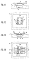
- Figures 1 and 2 are partial views, respectively of above and in section, of a memory card made by putting work of the process according to the invention.
- This card includes a body 1 made of insulating material, for example plastic, and provided with a cavity 2 in which is housed an integrated circuit 3 having on its face upper studs 4, one of which constitutes a ground stud 4a.
- a conduction range 5 comprising an internal part in the cavity 2 and an external part outside the latter, a first layer of dielectric varnish 6 covering the upper face of the integrated circuit 3 except for the pads 4 and 4a of this one, an adhesive tape 7 applied against the first layer of varnish 6 and against the body 1, around the cavity 2, conductors 8 provided on the adhesive tape 7 and electrically connected to the pads 4, a conductor 8a also provided on the adhesive tape and connected in turn to pad 4a and to the external part of the conduction range 5, read / write contacts 9 made up of specific areas conductors 8, a read / write contact 9a consisting of a particular area of the conductor 8a, and a second layer of varnish dielectric 10 covering the adhesive tape 7, the conductors 8,8a to the exception of their areas constituting the contacts of reading / writing 9,9a, and the parts of the first layer of varnish 6 which do not carry the conductors 8,8a.
- the cavity 2 has such a depth that the upper face of the varnish layer 6 is substantially in the plane of the upper face of the body 1 of the card. She has by elsewhere in plan dimensions slightly larger than those of integrated circuit.
- the conduction range 5 is formed by polymerization of a conductive ink made of a resin synthetic loaded with conductive pigments and capable of being deposited by screen printing.
- the adhesive tape 7 has holes 11 directly above the pads 4,4a of the integrated circuit 3 and a hole 12 directly above the part external of the conduction range 5, these different holes being filled by conductive ink deposited by screen printing on the ribbon adhesive 7 to form the conductors 8 and 8a.
- the varnishes used to form the first and second layers 6 and 10 are made of synthetic resins deposited by screen printing and can be identical or different, the varnish forming the first layer 6 having the particularity of being compatible with semiconductors and able to be insulated with a laser beam or a beam of ultraviolet rays, visible or infrared, or be abraded mechanically or chemically.
- Layer 6 is preferably deposited in its configuration final in one step. It could however be formed in several stages consisting successively of depositing on the face top of the integrated circuit 3 and on the pads 4.4 has a varnish polymerizable under the action of a light beam, for example a laser beam or a beam of ultraviolet rays, visible or infrared, to cover with a mask the parts of the varnish which are located directly above the pads 4,4a, to be exposed to the light beam the other parts of the varnish in order to polymerize them, to remove the mask, and to remove the non-polymerized parts of the varnish which cover the pads 4,4a.
- a light beam for example a laser beam or a beam of ultraviolet rays, visible or infrared
- the cavity 2 may have dimensions in plan slightly higher than those of integrated circuit 3. It is not indeed necessary that it has in plan precise dimensions for the reasons which will be recalled below.
- constituent ink could be deposited the conduction range 5 before making the cavity 2 by deformation of the body 1, for example by thermoforming or by ultrasonic forming.
- the adhesive tape 7 perfectly immobilizes the integrated circuit in the cavity, which prevents it from being made with precise plan dimensions.
- the adhesive tape is perforated at the advance, its holes 11 and 12 being distributed so as to correspond respectively to the pads 4,4a of the integrated circuit 3 and to the part outside of the conduction range 5. It can advantageously be provided with a succession of series of holes 11.12 distributed judiciously one after the other and be cut to length before or after several integrated circuits have been applied against him.
- the upper face of the layer of varnish 6 is coplanar with the upper face of the body 1 when the integrated circuit 3 is in place in the cavity 2.
- the conductive ink used is preferably deposited under its final configuration in one step. She could however first be deposited in the form of a layer having no discontinuity, then selectively removed so as to separate the ones of the others the assemblies each consisting of a conductor and the associated read / write contact.
- the selective removal of the conductive ink can be produced mechanically, for example at using a scraping stylus, thermally, for example under the action of a laser beam, or chemically.
- FIGS 11 to 14 illustrate the specific stages of the variant implementation of the method which has just been described.
- the perforated adhesive tape 7 is replaced by an unperforated adhesive tape 7a which is made of a material having the property of becoming locally conductive under the action of a pressure exerted on it perpendicular to its plane.
- the integrated circuit is then introduced into the cavity 2 of so that its studs face outwards, and we apply the free parts of the adhesive side of the adhesive tape 7a against the body 1 of the card, after which one exercises on the ribbon adhesive 7a, at the level of its parts overhanging the pads 4.4a of the integrated circuit and the external part of the conduction range 5, point pressures intended to make it locally conductive.
- Sure Figure 12 we have schematized the application of these forces by circles with the reference P.
- the 8.8a conductors are then produced (see Figures 13 and 14) as was done for the implementation of the method described in reference to Figures 1 to 10.
- the adhesive tape used for fixing the integrated circuit on the body of the card avoids the realization of cavity 2 with precise plan dimensions, ensures perfect immobilization of the integrated circuit in said cavity, allows making safe electrical connections increases resistance mechanics of these and makes the memory card capable of better resist the bending and torsional forces exerted on it during its use.
Landscapes
- Engineering & Computer Science (AREA)
- Computer Hardware Design (AREA)
- Microelectronics & Electronic Packaging (AREA)
- Physics & Mathematics (AREA)
- General Physics & Mathematics (AREA)
- Theoretical Computer Science (AREA)
- Credit Cards Or The Like (AREA)
Description
- la figure 1 est une vue de dessus schématique, partielle et avec arrachement d'une carte à mémoire obtenue par la mise en oeuvre du procédé conforme à l'invention ;
- la figure 2 est une vue en coupe schématique selon la ligne II-II de la figure 1 ;
- la figure 3 est une vue en coupe partielle montrant le circuit intégré après le dépôt de la première couche de vernis diélectrique ;
- la figure 4 est une vue partielle de dessus montrant le circuit intégré et la première couche de vernis visibles sur la figure 3 ;
- la figure 5 est une vue en coupe partielle montrant le corps de la carte après la réalisation de la cavité et de la plage de conduction ;
- la figure 6 est une vue partielle de dessus montrant le corps de la carte, la cavité et la plage de conduction visibles sur la figure 5 ;
- la figure 7 est une vue en coupe montrant le circuit intégré et le ruban adhésif fixés l'un contre l'autre par l'intermédiaire de la première couche de vernis, cet ensemble étant représenté au-dessus de la cavité du corps de la carte ;
- la figure 8 est une vue partielle de dessus montrant le circuit intégré dans la cavité et le ruban adhésif appliqué contre le corps de la carte ;
- la figure 9 est une vue partielle en coupe montrant le corps de la carte après le dépôt de l'encre conductrice sur le ruban adhésif ;
- la figure 10 est une vue partielle de dessus montrant le corps de la carte visible sur la figure 9 ; et
- les figures 11 à 14 illustrent une variante de réalisation du procédé conforme à l'invention et correspondent respectivement aux figures 7 à 10.
Claims (9)
- Procédé pour la fabrication d'une carte à mémoire comprenant un corps en matière isolante (1) pourvu d'un circuit intégré (3), ayant une surface supérieure recouverte d'une couche diélectrique (6) sauf sur des plots (4, 4a) que des conducteurs (8, 8a) en encre conductrice relient électriquement à des contacts de lecture/écriture (9, 9a), procédé comprenant une étape consistant à ménager une cavité (2) dans le corps (1) de la carte et les étapes d'appliquer l'une contre l'autre la couche diélectrique (6) et une face adhésive d'un ruban adhésif (7, 7a) dont les dimensions sont plus grandes que celles du circuit intégré, d'introduire le circuit intégré (3) dans la cavité (2), ses plots (4, 4a) étant tournés vers l'extérieur, d'appliquer la partie libre de la face adhésive du ruban adhésif (7, 7a) sur le corps (1) de la carte, à la périphérie de la cavité (2), de former les contacts de lecture/écriture (9, 9a) et les conducteurs (8, 8a) par dépôt d'une encre conductrice sur une autre face du ruban adhésif (7, 7a), lequel est apte à permettre des liaisons électriques entre les plots (4, 4a) et les conducteurs (8, 8a), et de former une seconde couche diélectrique (10) sur le ruban adhésif et sur les parties du dépôt d'encre qui ne constituent pas les contacts de lecture/écriture (9, 9a).
- Procédé selon la revendication 1, caractérisé en ce que le ruban adhésif (7) utilisé comporte des trous (11, 12) répartis de telle sorte qu'ils soient à l'aplomb des plots (4, 4a) du circuit intégré (3) lorsque ledit ruban adhésif et le circuit intégré (3) sont appliqués l'un contre l'autre, l'encre conductrice assurant les liaisons électriques en remplissant les trous.
- Procédé selon la revendication 1, caractérisé en ce que le ruban adhésif (7a) utilisé est apte à devenir localement conducteur de l'électricité sous l'action d'une pression (P) exercée sur lui perpendiculairement à son plan, et en ce qu'une pression est exercée sur les parties du ruban adhésif (7a) se trouvant à l'aplomb des plots (4, 4a), de sorte que les parties pressées du ruban adhésif (7a) relient électriquement l'encre conductrice avec les plots (4, 4a).
- Procédé selon la revendication 2 ou la revendication 3, caractérisé en ce que préalablement à l'étape d'introduction du circuit intégré (3) dans la cavité (2) il comporte l'étape de réaliser une plage de conduction (5) comprenant une partie interne située dans la cavité et une partie externe située hors de celle-ci, et en ce que le ruban adhésif (7, 7a) est apte à permettre une liaison électrique entre la partie externe de la plage de conduction (5) et l'un (8a) des conducteurs.
- Carte à mémoire comportant un corps en matière isolante (1) comprenant une cavité (2) dans laquelle est disposé un circuit intégré (3) ayant des plots (4, 4a) tournés vers l'extérieur et comportant une première couche diélectrique (6) s'étendant sur la face supérieure du circuit intégré sauf les plots (4, 4a) de celui-ci, des conducteurs (8, 8a) en résine synthétique conductrice reliant les plots (4, 4a) à des contacts de lecture/ écriture (9, 9a), et une seconde couche diélectrique (10) s'étendant sur les conducteurs (8, 8a), caractérisé en ce qu'un ruban adhésif (7, 7a) est fixé par une face adhésive à la première couche diélectrique (6) et au corps (1) autour de la cavité (2), et en ce que les conducteurs (8, 8a) ainsi que les contacts de lecture/écriture (9, 9a) auxquels ils sont reliés s'étendent sur une autre face du ruban adhésif (7, 7a).
- Carte à mémoire selon la revendication 5, caractérisée en ce que le ruban (7) comporte des trous (11, 12) à l'aplomb des plots (4, 4a) du circuit intégré (3) et en ce que les conducteurs (8, 8a) s'étendent dans les trous.
- Carte à mémoire selon la revendication 5, caractérisée en ce que le ruban (7a) comporte des parties conductrices à l'aplomb des plots (4, 4a) du circuit intégré (3) et en ce que les conducteurs (8, 8a) s'étendent sur ces parties conductrices.
- Carte à mémoire selon la revendication 6 ou la revendication 7, caractérisée en ce qu'elle comporte une plage de conduction (5) comprenant une partie interne située dans la cavité (2) en contact avec le circuit intégré, et une partie externe située hors de la cavité, en liaison électrique avec l'un (8a) des conducteurs.
- Carte à mémoire selon la revendication 8, caractérisée en ce que la plage conductrice (5) est en résine synthétique conductrice.
Priority Applications (4)
| Application Number | Priority Date | Filing Date | Title |
|---|---|---|---|
| FR919114899A FR2684471B1 (fr) | 1991-12-02 | 1991-12-02 | Procede de fabrication d'une carte a memoire et carte a memoire ainsi obtenue. |
| DE69327308T DE69327308T2 (de) | 1993-06-02 | 1993-06-02 | Verfahren zur Herstellung einer Speicherkarte und nach diesem Verfahren hergestellte Speicherkarte |
| EP93401397A EP0627707B1 (fr) | 1991-12-02 | 1993-06-02 | Procédé de fabrication d'une carte à mémoire et carte à mémoire ainsi obtenue |
| AT93401397T ATE187829T1 (de) | 1993-06-02 | 1993-06-02 | Verfahren zur herstellung einer speicherkarte und nach diesem verfahren hergestellte speicherkarte |
Applications Claiming Priority (2)
| Application Number | Priority Date | Filing Date | Title |
|---|---|---|---|
| FR919114899A FR2684471B1 (fr) | 1991-12-02 | 1991-12-02 | Procede de fabrication d'une carte a memoire et carte a memoire ainsi obtenue. |
| EP93401397A EP0627707B1 (fr) | 1991-12-02 | 1993-06-02 | Procédé de fabrication d'une carte à mémoire et carte à mémoire ainsi obtenue |
Publications (2)
| Publication Number | Publication Date |
|---|---|
| EP0627707A1 EP0627707A1 (fr) | 1994-12-07 |
| EP0627707B1 true EP0627707B1 (fr) | 1999-12-15 |
Family
ID=26134694
Family Applications (1)
| Application Number | Title | Priority Date | Filing Date |
|---|---|---|---|
| EP93401397A Expired - Lifetime EP0627707B1 (fr) | 1991-12-02 | 1993-06-02 | Procédé de fabrication d'une carte à mémoire et carte à mémoire ainsi obtenue |
Country Status (2)
| Country | Link |
|---|---|
| EP (1) | EP0627707B1 (fr) |
| FR (1) | FR2684471B1 (fr) |
Families Citing this family (18)
| Publication number | Priority date | Publication date | Assignee | Title |
|---|---|---|---|---|
| US6817532B2 (en) * | 1992-02-12 | 2004-11-16 | Lenscard U.S., Llc | Wallet card with built-in light |
| FR2726106B1 (fr) * | 1994-10-21 | 1996-11-29 | Solaic Sa | Carte electronique utilisable avec un lecteur de cartes sans contact et un lecteur de cartes a contacts |
| FR2735284B1 (fr) * | 1995-06-12 | 1997-08-29 | Solaic Sa | Puce pour carte electronique revetue d'une couche de matiere isolante et carte electronique comportant une telle puce |
| FR2736453B1 (fr) * | 1995-07-07 | 1997-08-08 | Gemplus Card Int | Support portable a microcircuit, notamment carte a puce, et procede de fabrication dudit support |
| FR2736740A1 (fr) * | 1995-07-11 | 1997-01-17 | Trt Telecom Radio Electr | Procede de production et d'assemblage de carte a circuit integre et carte ainsi obtenue |
| FR2741009B1 (fr) * | 1995-11-15 | 1997-12-12 | Solaic Sa | Carte a circuit integre et module a circuit integre |
| DE19600388C2 (de) * | 1996-01-08 | 2000-03-09 | Orga Kartensysteme Gmbh | Chipkarte |
| FR2744271A1 (fr) * | 1996-01-30 | 1997-08-01 | Solaic Sa | Carte a memoire et procede de fabrication d'une telle carte |
| FR2748335A1 (fr) * | 1996-05-06 | 1997-11-07 | Solaic Sa | Carte a memoire et procede de fabrication d'une telle carte |
| FR2753305B1 (fr) * | 1996-09-12 | 1998-11-06 | Schlumberger Ind Sa | Procede de fabrication d'un ensemble de modules electroniques pour cartes a memoire sans contact |
| FR2754618B1 (fr) * | 1996-10-14 | 1998-12-11 | Solaic Sa | Carte a memoire a compensation dimensionnelle |
| DE19721918C2 (de) * | 1997-05-26 | 2001-10-31 | Orga Kartensysteme Gmbh | Chipkarte und Verfahren zu deren Herstellung |
| FR2779255B1 (fr) * | 1998-05-27 | 2001-10-12 | Gemplus Card Int | Procede de fabrication d'un dispositif electronique portable comportant au moins une puce de circuit integre |
| FR2789505B1 (fr) * | 1999-02-08 | 2001-03-09 | Gemplus Card Int | Procede de fabrication de support de memorisation portable de type carte a puce |
| FR2818802B1 (fr) * | 2000-12-21 | 2003-11-28 | Gemplus Card Int | Connexion par isolant decoupe et cordon imprime en plan |
| US6998533B2 (en) * | 2002-04-11 | 2006-02-14 | Koninklijke Philips Electronics N.V. | Electronic device and method of manufacturing same |
| DE102005038132B4 (de) | 2005-08-11 | 2008-04-03 | Infineon Technologies Ag | Chipmodul und Chipkarte |
| EP2824704A1 (fr) * | 2013-07-12 | 2015-01-14 | Gemalto SA | Module électronique et son procédé de fabrication |
Family Cites Families (4)
| Publication number | Priority date | Publication date | Assignee | Title |
|---|---|---|---|---|
| DE3153769C2 (de) * | 1981-04-14 | 1995-10-26 | Gao Ges Automation Org | Trägerelement zum Einbau in Ausweiskarten |
| JPS62107391A (ja) * | 1985-11-06 | 1987-05-18 | Nippon Texas Instr Kk | 情報記憶媒体 |
| FR2632100B1 (fr) * | 1988-05-25 | 1992-02-21 | Schlumberger Ind Sa | Procede de realisation d'une carte a memoire electronique et cartes a memoire electronique obtenue par la mise en oeuvre dudit procede |
| CA2027823C (fr) * | 1989-10-31 | 1994-11-08 | Tomoshige Oka | Carte possedant un module de circuit integre et un ouverture de decharge a l'air |
-
1991
- 1991-12-02 FR FR919114899A patent/FR2684471B1/fr not_active Expired - Fee Related
-
1993
- 1993-06-02 EP EP93401397A patent/EP0627707B1/fr not_active Expired - Lifetime
Also Published As
| Publication number | Publication date |
|---|---|
| FR2684471A1 (fr) | 1993-06-04 |
| EP0627707A1 (fr) | 1994-12-07 |
| FR2684471B1 (fr) | 1994-03-04 |
Similar Documents
| Publication | Publication Date | Title |
|---|---|---|
| FR2684471A1 (fr) | Procede de fabrication d'une carte a memoire et carte a memoire ainsi obtenue. | |
| EP0344058B1 (fr) | Procédé de réalisation d'une carte à mémoire électronique et carte à mémoire électronique obtenue par la mise en oeuvre dudit procédé | |
| EP1062635B1 (fr) | Procede de fabrication de cartes sans contact | |
| EP0753827B1 (fr) | Procédé de production et d'assemblage de carte à circuit intégré et carte ainsi obtenue | |
| EP1141887B1 (fr) | Procede de fabrication de carte a puce sans contact | |
| EP1101193B1 (fr) | Antenne ajouree pour carte a circuit integre, et carte a circuit integre comprenant une telle antenne | |
| EP1076882B1 (fr) | Carte a circuit integre comportant un bornier d'interface et procede de fabrication d'une telle carte | |
| WO1996042109A1 (fr) | Puce pour carte electronique revetue d'une couche de matiere isolante et carte electronique comportant une telle puce | |
| WO1997048074A1 (fr) | Carte a memoire et procede de fabrication d'une telle carte | |
| EP0954021B1 (fr) | Procédé de réalisation d'un composant électronique | |
| FR2738077A1 (fr) | Micro-boitier electronique pour carte a memoire electronique et procede de realisation | |
| EP0305267B1 (fr) | Procédé pour la réalisation d'un ensemble de motifs électriquement conducteurs sur une surface isolante de forme complexe | |
| FR2671417A1 (fr) | Procede pour la fabrication d'une carte a memoire et carte a memoire ainsi obtenue . | |
| EP0969410B1 (fr) | Carte à microcircuit incluant une antenne | |
| EP0195871A1 (fr) | Connecteur électrique multipolaire et son procédé de fabrication | |
| FR2671416A1 (fr) | Procede pour la fabrication d'une carte a memoire et carte a memoire ainsi obtenue. | |
| FR2803413A1 (fr) | Element de carte a circuit integre monte en flip-chip | |
| FR2777675A1 (fr) | Procede de fabrication d'une carte a microcircuit et carte a microcircuit obtenue par mise en oeuvre de ce procede | |
| FR2671418A1 (fr) | Procede pour la fabrication d'une carte a memoire et carte a memoire ainsi obtenue. | |
| FR2741009A1 (fr) | Carte a circuit integre et module a circuit integre | |
| WO1999054845A1 (fr) | Procede de realisaiton d'une entite decorative sur une carte du type a circuit integre | |
| FR3001332A1 (fr) | Procede de fabrication d'un corps de carte a puce | |
| FR2744819A1 (fr) | Carte a circuit integre sans contact, procede et outillage pour la fabrication d'une telle carte | |
| FR2744271A1 (fr) | Carte a memoire et procede de fabrication d'une telle carte | |
| FR2545977A1 (fr) | Dispositif de communication |
Legal Events
| Date | Code | Title | Description |
|---|---|---|---|
| PUAI | Public reference made under article 153(3) epc to a published international application that has entered the european phase |
Free format text: ORIGINAL CODE: 0009012 |
|
| AK | Designated contracting states |
Kind code of ref document: A1 Designated state(s): AT BE CH DE DK ES GB GR IE IT LI LU MC NL PT SE |
|
| 17P | Request for examination filed |
Effective date: 19950504 |
|
| GRAG | Despatch of communication of intention to grant |
Free format text: ORIGINAL CODE: EPIDOS AGRA |
|
| 17Q | First examination report despatched |
Effective date: 19980921 |
|
| GRAG | Despatch of communication of intention to grant |
Free format text: ORIGINAL CODE: EPIDOS AGRA |
|
| RAP1 | Party data changed (applicant data changed or rights of an application transferred) |
Owner name: SCHLUMBERGER SYSTEMES |
|
| GRAG | Despatch of communication of intention to grant |
Free format text: ORIGINAL CODE: EPIDOS AGRA |
|
| GRAH | Despatch of communication of intention to grant a patent |
Free format text: ORIGINAL CODE: EPIDOS IGRA |
|
| GRAH | Despatch of communication of intention to grant a patent |
Free format text: ORIGINAL CODE: EPIDOS IGRA |
|
| GRAA | (expected) grant |
Free format text: ORIGINAL CODE: 0009210 |
|
| AK | Designated contracting states |
Kind code of ref document: B1 Designated state(s): AT BE CH DE DK ES GB GR IE IT LI LU MC NL PT SE |
|
| PG25 | Lapsed in a contracting state [announced via postgrant information from national office to epo] |
Ref country code: SE Free format text: THE PATENT HAS BEEN ANNULLED BY A DECISION OF A NATIONAL AUTHORITY Effective date: 19991215 Ref country code: NL Free format text: LAPSE BECAUSE OF FAILURE TO SUBMIT A TRANSLATION OF THE DESCRIPTION OR TO PAY THE FEE WITHIN THE PRESCRIBED TIME-LIMIT Effective date: 19991215 Ref country code: IT Free format text: LAPSE BECAUSE OF FAILURE TO SUBMIT A TRANSLATION OF THE DESCRIPTION OR TO PAY THE FEE WITHIN THE PRE;WARNING: LAPSES OF ITALIAN PATENTS WITH EFFECTIVE DATE BEFORE 2007 MAY HAVE OCCURRED AT ANY TIME BEFORE 2007. THE CORRECT EFFECTIVE DATE MAY BE DIFFERENT FROM THE ONE RECORDED.SCRIBED TIME-LIMIT Effective date: 19991215 Ref country code: GR Free format text: LAPSE BECAUSE OF NON-PAYMENT OF DUE FEES Effective date: 19991215 Ref country code: ES Free format text: THE PATENT HAS BEEN ANNULLED BY A DECISION OF A NATIONAL AUTHORITY Effective date: 19991215 Ref country code: AT Free format text: LAPSE BECAUSE OF FAILURE TO SUBMIT A TRANSLATION OF THE DESCRIPTION OR TO PAY THE FEE WITHIN THE PRESCRIBED TIME-LIMIT Effective date: 19991215 |
|
| REF | Corresponds to: |
Ref document number: 187829 Country of ref document: AT Date of ref document: 20000115 Kind code of ref document: T |
|
| REG | Reference to a national code |
Ref country code: CH Ref legal event code: EP |
|
| REF | Corresponds to: |
Ref document number: 69327308 Country of ref document: DE Date of ref document: 20000120 |
|
| GBT | Gb: translation of ep patent filed (gb section 77(6)(a)/1977) |
Effective date: 20000111 |
|
| REG | Reference to a national code |
Ref country code: IE Ref legal event code: FG4D |
|
| PG25 | Lapsed in a contracting state [announced via postgrant information from national office to epo] |
Ref country code: PT Free format text: LAPSE BECAUSE OF FAILURE TO SUBMIT A TRANSLATION OF THE DESCRIPTION OR TO PAY THE FEE WITHIN THE PRESCRIBED TIME-LIMIT Effective date: 20000315 Ref country code: DK Free format text: LAPSE BECAUSE OF FAILURE TO SUBMIT A TRANSLATION OF THE DESCRIPTION OR TO PAY THE FEE WITHIN THE PRESCRIBED TIME-LIMIT Effective date: 20000315 |
|
| PG25 | Lapsed in a contracting state [announced via postgrant information from national office to epo] |
Ref country code: LU Free format text: LAPSE BECAUSE OF NON-PAYMENT OF DUE FEES Effective date: 20000602 |
|
| NLV1 | Nl: lapsed or annulled due to failure to fulfill the requirements of art. 29p and 29m of the patents act | ||
| PG25 | Lapsed in a contracting state [announced via postgrant information from national office to epo] |
Ref country code: MC Free format text: THE PATENT HAS BEEN ANNULLED BY A DECISION OF A NATIONAL AUTHORITY Effective date: 20000630 Ref country code: LI Free format text: LAPSE BECAUSE OF NON-PAYMENT OF DUE FEES Effective date: 20000630 Ref country code: CH Free format text: LAPSE BECAUSE OF NON-PAYMENT OF DUE FEES Effective date: 20000630 Ref country code: BE Free format text: LAPSE BECAUSE OF NON-PAYMENT OF DUE FEES Effective date: 20000630 |
|
| PLBE | No opposition filed within time limit |
Free format text: ORIGINAL CODE: 0009261 |
|
| STAA | Information on the status of an ep patent application or granted ep patent |
Free format text: STATUS: NO OPPOSITION FILED WITHIN TIME LIMIT |
|
| PG25 | Lapsed in a contracting state [announced via postgrant information from national office to epo] |
Ref country code: IE Free format text: LAPSE BECAUSE OF NON-PAYMENT OF DUE FEES Effective date: 20001109 |
|
| 26N | No opposition filed | ||
| REG | Reference to a national code |
Ref country code: IE Ref legal event code: FD4D |
|
| BERE | Be: lapsed |
Owner name: SCHLUMBERGER SYSTEMES Effective date: 20000630 |
|
| REG | Reference to a national code |
Ref country code: CH Ref legal event code: PL |
|
| REG | Reference to a national code |
Ref country code: GB Ref legal event code: IF02 |
|
| PGFP | Annual fee paid to national office [announced via postgrant information from national office to epo] |
Ref country code: GB Payment date: 20020529 Year of fee payment: 10 |
|
| PGFP | Annual fee paid to national office [announced via postgrant information from national office to epo] |
Ref country code: DE Payment date: 20020610 Year of fee payment: 10 |
|
| PG25 | Lapsed in a contracting state [announced via postgrant information from national office to epo] |
Ref country code: GB Free format text: LAPSE BECAUSE OF NON-PAYMENT OF DUE FEES Effective date: 20030602 |
|
| PG25 | Lapsed in a contracting state [announced via postgrant information from national office to epo] |
Ref country code: DE Free format text: LAPSE BECAUSE OF NON-PAYMENT OF DUE FEES Effective date: 20040101 |
|
| GBPC | Gb: european patent ceased through non-payment of renewal fee |
Effective date: 20030602 |