EP0626727A2 - Thin-film wiring layout for a non-planar thin-film structure - Google Patents
Thin-film wiring layout for a non-planar thin-film structure Download PDFInfo
- Publication number
- EP0626727A2 EP0626727A2 EP94480032A EP94480032A EP0626727A2 EP 0626727 A2 EP0626727 A2 EP 0626727A2 EP 94480032 A EP94480032 A EP 94480032A EP 94480032 A EP94480032 A EP 94480032A EP 0626727 A2 EP0626727 A2 EP 0626727A2
- Authority
- EP
- European Patent Office
- Prior art keywords
- vias
- layers
- arrangement
- thin
- lines
- Prior art date
- Legal status (The legal status is an assumption and is not a legal conclusion. Google has not performed a legal analysis and makes no representation as to the accuracy of the status listed.)
- Withdrawn
Links
Images


Classifications
-
- H—ELECTRICITY
- H01—ELECTRIC ELEMENTS
- H01L—SEMICONDUCTOR DEVICES NOT COVERED BY CLASS H10
- H01L23/00—Details of semiconductor or other solid state devices
- H01L23/52—Arrangements for conducting electric current within the device in operation from one component to another, i.e. interconnections, e.g. wires, lead frames
- H01L23/538—Arrangements for conducting electric current within the device in operation from one component to another, i.e. interconnections, e.g. wires, lead frames the interconnection structure between a plurality of semiconductor chips being formed on, or in, insulating substrates
- H01L23/5384—Conductive vias through the substrate with or without pins, e.g. buried coaxial conductors
-
- H—ELECTRICITY
- H01—ELECTRIC ELEMENTS
- H01L—SEMICONDUCTOR DEVICES NOT COVERED BY CLASS H10
- H01L23/00—Details of semiconductor or other solid state devices
- H01L23/52—Arrangements for conducting electric current within the device in operation from one component to another, i.e. interconnections, e.g. wires, lead frames
- H01L23/538—Arrangements for conducting electric current within the device in operation from one component to another, i.e. interconnections, e.g. wires, lead frames the interconnection structure between a plurality of semiconductor chips being formed on, or in, insulating substrates
- H01L23/5386—Geometry or layout of the interconnection structure
-
- H—ELECTRICITY
- H01—ELECTRIC ELEMENTS
- H01L—SEMICONDUCTOR DEVICES NOT COVERED BY CLASS H10
- H01L2924/00—Indexing scheme for arrangements or methods for connecting or disconnecting semiconductor or solid-state bodies as covered by H01L24/00
- H01L2924/0001—Technical content checked by a classifier
- H01L2924/0002—Not covered by any one of groups H01L24/00, H01L24/00 and H01L2224/00
-
- H—ELECTRICITY
- H01—ELECTRIC ELEMENTS
- H01L—SEMICONDUCTOR DEVICES NOT COVERED BY CLASS H10
- H01L2924/00—Indexing scheme for arrangements or methods for connecting or disconnecting semiconductor or solid-state bodies as covered by H01L24/00
- H01L2924/095—Indexing scheme for arrangements or methods for connecting or disconnecting semiconductor or solid-state bodies as covered by H01L24/00 with a principal constituent of the material being a combination of two or more materials provided in the groups H01L2924/013 - H01L2924/0715
- H01L2924/097—Glass-ceramics, e.g. devitrified glass
- H01L2924/09701—Low temperature co-fired ceramic [LTCC]
-
- H—ELECTRICITY
- H01—ELECTRIC ELEMENTS
- H01L—SEMICONDUCTOR DEVICES NOT COVERED BY CLASS H10
- H01L2924/00—Indexing scheme for arrangements or methods for connecting or disconnecting semiconductor or solid-state bodies as covered by H01L24/00
- H01L2924/30—Technical effects
- H01L2924/301—Electrical effects
- H01L2924/3011—Impedance
Definitions
- This invention relates to a wiring layout, and more particularly, to a thin-film wiring arrangement for a non-planar structure.
- VLSI semiconductor circuits are generally manufactured by depositing and patterning conductive and non-conductive layers on a substrate and by stacking these layers one on top of the other. As VLSI circuits become more sophisticated and more complex, the number of stacked layers or planes increases, thereby creating planarity problems. Much attention has been directed to solving this problem.
- J. L. Freeman et al, in US-A-5,149,674 provide a method for planarizing bonding and probe pads, and more particularly, multi-layer metal pads, in relation to the interior of the semiconductor VLSI devices.
- the dimple on the surface of a via causes a reduction in the surface area available for contact between vias, thus eliminating the use of stacked vias for process and reliabilities reasons. Moreover, when vias are stacked in a column, the effect of these dimples tends to compound, leading to a non-planar structure at the top surface.
- the design of the wiring layer and reference layers is critical since dielectric non-planarity introduces waviness in the lines that changes the electrical characteristics.
- the only viable method for maintaining uniform line characteristics is to have fixed areas in the layout for lines and fixed channels for wiring. This technique is used in a planar process to achieve uniformity by stacking the vias, thereby allocating specific areas for the vias and lines. Vias, however, in a non-planar process cannot be stacked and have interfaces with the lines, thus producing non-uniformity both in the physical and electrical characteristics of the structure.
- the present invention is a an arrangement of vias in a thin-film structure, comprising a plurality of thin-film layers stacked on top of each other, the layers having wiring lines and a plurality of vias, the vias providing a connection between a line in one of the layers to a line in another of the layers; at least one of the vias in one of the layers being offset from and in contact with at least a via in a subsequent layer, and wherein a plurality of the connecting vias are positioned in a non-linear arrangement.
- Thin-films provide a large variety of functions, such as limiting delta-I noise, by introducing a low inductance path to decoupling capacitors for large off-chip switching activity, high density wiring, small propagation delays and increased wirability for the redistribution and connection of wires.
- a good thin-film design is necessary to support critical nets and reduce noise, since these control the cycle time of a machine.
- FIG. 1 illustrates a cross section of a prior art arrangement of stacked vias using a planar thin-film process. Shown is a structure consisting of a substrate 14, upon which various thin-film layers are placed one on top of the other to provide the necessary wiring.
- the thin-film wiring consists of a bottom reference plane 9, two layers 10 and 11 providing, respectively, X and Y wiring, preferably with lines orthogonal to each other, and a top reference plane 12.
- the bottom reference plane 9 is separated from the substrate by an insulator or dielectric layer 15.
- the reference planes as well as the two wiring planes 9 and 10 are separated from each other by dielectric layers 16, 17 and 18.
- vias provide vertical interconnections between the various metal layers.
- the reference planes 9 and 12 are voltage or reference planes that supply power and current to the chips as well as provide a return path for the wiring layers 10 and 11, thereby converting the wires into transmission lines that can support electrical signals for communication.
- the reference planes also provide shielding for the wiring layers, thereby providing a controlled electrical environment, limiting coupled noise and ensuring first incident switching of the receivers.
- the use of two reference planes has the added advantage of providing a short inductive path from any decoupling capacitors attached on the top surface to the drivers in the chips, which reduces delta I noise. Due to the shorter inductive path provided by the reference planes, it is now possible to support additional simultaneously switching drivers.
- the conductor and dielectric levels are built sequentially.
- the dielectric layer is deposited and the vias are formed.
- the conductor layer is then deposited.
- This conductor layer follows the contours of the underlying dielectric layer and, hence, the process is called the conformal via process.
- This leads to a dimple at the via location whose dimensions are equal to or less than the dimensions of the via itself.
- the dimensions of the dimple depends on the conductor metallization process and the thickness of the conductor metal.
- the conductor metal is equal to or less than the thickness of the dielectric level.
- the cross section shown in FIG. 1A assumes a planar process that includes planarizing all dielectric and metal layers.
- a substrate such as a glass ceramic or alumina material, which may or may not support any wiring in it.
- the substrate supports wiring.
- Layer 13 represents a metal layer (capture pad) that provides electrical connections between the vias in the thin-film and vias in the substrate. This is required due to substrate via distortion that provides an uncertainty in the placement of the substrate via.
- Layer 13 is typically 2-4 ⁇ m thick.
- V ias 1, 2,..., 8 are conductive vias that provide vertical interconnections between various layers in the thin film wiring.
- Layers 15, 16, 17 and 18 are dielectric layers that ensure no electrical contact among the conductive layers 9, 10, 11, and 12.
- Layers 9 and 12 are reference planes comprising X and Y conductors, which are electrically connected on the same layer. Due to the large amount of metal present in those layers, they can act as voltage planes and supply current to the chips. Layers 10 and 11 are, respectively, X and Y wiring layers which supply the electrical interconnections. The X and Y direction wiring may be interchanged if necessary with no impact on the electrical characteristics. Since the reference planes 9 and 12 are physically in close proximity to wiring layers 10 and 11, they act as a return path for the wiring, thus converting the wires in 10 and 11 into transmission lines.
- the electrical characteristics of the transmission lines in 10 and 11 can be varied by changing the physical position of the lines with respect to the conductors in the reference planes 9 and 12. For example, lines in 10 could be moved between two conductors in 9 and 12 to reduce the capacitance, while increasing the inductance and, hence, the impedance of the lines. Practitioners of the art will readily appreciate that since the process is planar, all lines have the same electrical characteristics, since they all see an identical electrical configuration. This is true irrespective of the wiring and reference plane layout due to the planar environment.
- vias provide vertical interconnections.
- vias 1, 2, ..., and 8 provide vertical connections between 14 and the chip which is joined to the top of the thin-film structure. These vias could also provide vertical connections between 10 and 11 to change the direction of the wiring.
- the process since the process is planar, all vias are stacked and, thus, vertically aligned. This provides a uniform height to all the parts of the package, i.e., to all the chips positioned on the top surface. It also provides a good electrical and mechanical contact surface for attaching the chips.
- the planar process provides two critical characteristics that are essential to any design, namely:
- Fig 1B illustrates a cross section of a thin-film layout similar to Fig 1A, with the difference that a non-planar process is used, as opposed to a planar process.
- the non-planar process implies eliminating all planarizing steps, thereby reducing the cost of manufacture.
- a non-planar process is clearly the preferred approach in industry due to its reduced cost. Since the planarization step is completely eliminated at all levels, the process produces a local and global non-planarity on the entire structure.
- Non-planarity however, has some serious drawbacks, such as a reduction in reliability, electrical variations, etc., some of which are discussed hereinafter.
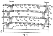
- vias 19, 20,..., and 26 provide vertical connections; 27 and 30 are the reference planes; 28 and 29 are, respectively, the X and Y wiring layers; 31, 32, 33 and 34 are the insulator layers; 13 is a capture pad layer; and 14 the substrate.
- the non-planar process produces a dimple or void on the via surface due to an uneven plate-up of the conductive metal vias 19, 20, ..., and 26. This forces the vias to be rearranged in a non-stacked fashion so that no via aligns itself on top of another via to avoid the possibility of opens caused by the thinning of the metal on the walls of the void.
- vias 19, 20, ..., and 26 are offset laterally in a staircase or linear arrangement. This technique, though necessary, creates three problems, namely:
- the present invention makes use of the non-planar process to produce a structure that contains all the features of a planar process, i.e., all electrical, mechanical and reliability characteristics.
- FIG. 1C a cross section of the structure in accordance with the present invention is shown.
- the thin-film structure is fabricated using a non-planar process such as the one used in Fig 1B. Shown in FIG. 1C are: a substrate 14, a capture pad 13, conductive vias 19-26, reference planes 27 and 30, the X and Y wiring 28 and 29, respectively, and insulators 31, 32, 33, and 34.
- the function performed by the various parts of the structure are the same as in FIGS. 1A and 1B.
- the use of the non-planar process produces a dimple on the surface of the vias due to uneven plate-up during fabrication. Hence the vias have to be staggered from one another.
- the structure of FIG. 1C uses, on each layer, a two dimensional staggering scheme coupled with a vertical non-stacking method, to provide a via structure that is characterized in that:
- Fig. 1C further highlights all the wires in the X and the Y layers, respectively, overlapping the corresponding conductors in the planes 27 and 30. Due to the complete overlap of the conductive layers 28 and 27 (29 and 30) separated by a dielectric layer 32 (34), the wires always follow the corresponding return conductors in the reference plane (or vice versa). Therefore, the dielectric will keep a uniform thickness between the wires and the reference planes. This technique reduces interlevel shorts caused by dielectric thinning, and also maintains the electrical characteristics of the lines constant due to a uniform capacitance along the wire length. Hence the present invention eliminates the disadvantages of the non-planar process and produces a wiring structure with the same characteristics of a planar process.
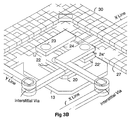
- Fig. 2 shows a via staggering scheme that connects the substrate via to the chips on the top surface. This method is specially relevant to the voltage vias that supply current to the chips. A similar scheme will be described later for the signal vias.
- the capture pad layer is formed on the substrate (13) which connects the substrate vias to the thin film via (19).
- the capture pad layer is generally formed using a sub-etch process and is generally 2-4 um thick, large enough to capture the substrate vias based on worst case tolerances.
- a polymer layer (31) is deposited on the capture pad layer to act as an insulator to separate the thin film reference plane (27) from the substrate.
- the layer thickness of 31 is typically around 9-12 um.
- This thickness is required to reduce the additional capacitance introduced by the proximity of the capture pad 13 to the reference plane 27 and due to the self planarizing property of the thick dielectric.
- Two conductive vias (19) make vertical contact between layer 13 and layer 20 above it. As shown in the figure, a dimple or valley is created on the surface of the two vias due to the non-planar process.
- Metal 20 is electroplated onto the top surface of the via on the same layer as the bottom reference plane 27 in Fig. 1C.
- Metal layer 20 can be of the same size, smaller or larger than metal layer 13. This is particularly important since layer 20 completely or partially overlaps the layer 13 that provides planarity in areas of overlap, except where the vias 19 meet the metal layer 20.
- the next set of vias 21 are laterally displaced with respect to vias 19 so that they do not align on top of the dimples of vias 19.
- vias 21 are placed within the area of metal pad 20.
- Vias 21 provide vertical contact between the metal layers 20 and 22.
- Metal pad 22 is deposited in such a way that it completely overlaps metal pad 20 producing planarity in the overlap areas except at the dimples formed by vias 21.
- a similar arrangement is used for vias 23, 25 and metal pads 24 and 26. Using the present arrangement, the surface of 26 is planar in all areas having horizontal pads 20, 22 and 24 beneath them. Surface 26 still has a dimple on the surface formed by vias 25.
- the next set of vias 35 are again laterally displaced, and a large pad 36 is formed above it that represents the micro-socket for attaching the chips.
- the top surface (36) at the micro-socket location is planar, and hence it provides an even surface for attaching the chip.
- two vias are provided at each via level to increase reliability through current sharing. This is particularly significant since the redundancy makes the process robust by increasing yield for via opens. If necessary, one large via could be provided at each via level, and a similar arrangement can be used.
- metal pad 20 is shown to be larger than metal pad 26. This is because the metal pad 20 is connected laterally to the bottom reference plane 27.
- the via arrangement shown in Fig. 2 represents a voltage via where the redundancy has been used to make the process more robust.
- the via redundancy is not required for signal vias due to the small current carried by signal vias.
- the two vias need not be physically connected on layers 22 and 24 for signal vias which as will be shown hereinafter, thus increasing wirability.
- a similar voltage via arrangement with metal pad 26 connected to the top reference plane (metal pad 26 larger than pad 20) could be used for a different voltage level for the reference plane 30.
- the via arrangement for a signal through via is shown in Fig. 3A.
- the basic principle of the via arrangement is similar to FIG. 2. However, the difference is that the two vias are electrically separated on metal pad layers 22 and 24. As before, the metal pads always overlap the metal pads beneath, thus ensuring planarity.
- vias 21, 23 and 25 are programmable and may or may not be formed based on the wiring.
- Metal pads 22, 24 and vias 23 are used as translation layers to change wiring directions from X to Y or from Y to X.
- An example of the use of the via arrangement for a change in direction of the wiring is shown in Fig. 3B.
- vias 25 have not been formed (programmable) and, hence, the connections to a micro-socket do not have any connection to metal pads 24.
- a wire on X can now connect to one of the metal pads 22, translate onto metal pad 24 through via 23, connect to a wire in the Y direction, and then drop onto an X wire in a different channel by means of an interstitial via that is positioned at alternate intersections of the X,Y wiring.
- a similar concept can be used whereby a Y wire connects to a metal pad 24, translates onto the metal pad 22 through via 23 which can then connect to an X or a Y wire in a different channel through an interstitial via.
- two sets of vias at signal locations can be used as direction changers, which considerably increase wirability.
- the redundant via arrangement in FIG. 2 can be used, but with the difference that metal pads 20 and 26 are not connected to the reference plane.
- the via arrangement which is based on a laterally displaced vertical column concept has three basic uses, namely:
- the bottom reference plane 27 is comprised of a series of X and Y conductors that are electrically connected with openings provided for the through vias to contact the chips. This scheme is required from a process stand-point due to outgassing of the polymer because of thermal cycling. A solid plane cannot be used for reference layers 27 and 30 since outgassing causes metal to blister or break.
- the X wiring layer 28c is deposited in such a way that the wires overlap the corresponding X conductors of 27. In the preferred embodiment, the conductors in 27 are wider than the wires in 28.
- This overlapping scheme ensures that a uniform dielectric layer always exists between the X wires and the corresponding conductors of 27, thus maintaining the same capacitance along the wire length.
- Wiring layer 29 is next deposited such that they overlap the Y conductors of 30.
- Reference layer 30 is formed next with the X and Y conductors overlapping the X and Y wires. Using this method, the top reference plane 30 always follows the corresponding Y wires 29, thus maintaining the same capacitance along the wire length. Though 29 has crests and valleys with respect to 27, and 30 has crests and valleys with respect to 28, the reference planes are farther away and, hence, have a small impact on the electrical characteristics of the line.
- the structure described in this invention can be used to built multiple plane pairs of thin film, vertically above each other.
- the top layer of the thin film structure will be easily planarized due to uniform height of the top vias and multiple layers using a similar layout described in this invention could be built. Due to the present layout, the electrical characteristics in the two plane pairs are identical. Hence multi le plane pairs could be built by introducing just one planarization per plane pair.
Abstract
Description
- This invention relates to a wiring layout, and more particularly, to a thin-film wiring arrangement for a non-planar structure.
- Very large scale integrated (VLSI) semiconductor circuits are generally manufactured by depositing and patterning conductive and non-conductive layers on a substrate and by stacking these layers one on top of the other. As VLSI circuits become more sophisticated and more complex, the number of stacked layers or planes increases, thereby creating planarity problems. Much attention has been directed to solving this problem. By way of example, J. L. Freeman et al, in US-A-5,149,674 provide a method for planarizing bonding and probe pads, and more particularly, multi-layer metal pads, in relation to the interior of the semiconductor VLSI devices.
- Although planarity has proven to present distinct advantages by better controlling critical dimensions and by more evenly distributing conductive and dielectric material, cost considerations may dictate maintaining a non-planar environment. This is particularly true for thin-film structures, and it is most evident in areas that surround vias. Vias are known in the art to establish electrical contact between wiring lines in one layer to wiring lines in some other layer, and to provide an external interface for interconnections. This contact can be maintained even if the lines to be contacted are not in adjacent planes, in which case contact is usually achieved by stacking vias one on top of the other. The process of stacking vias in a non-planar environment presents a problem in that vias display a dimple on the top surface usually caused by uneven plate-up of the metal features. The dimple on the surface of a via causes a reduction in the surface area available for contact between vias, thus eliminating the use of stacked vias for process and reliabilities reasons. Moreover, when vias are stacked in a column, the effect of these dimples tends to compound, leading to a non-planar structure at the top surface.
- Adding to the non-planarity problems, the manner in which a via column is layed out results in lines having non-uniform electrical characteristics due to the presence or absence of reference planes beneath or above the transmission lines. This unevenness causes a significant decrease in the uniformity of lines per channel for long wiring lengths.
- Due to a non-planar environment, the design of the wiring layer and reference layers is critical since dielectric non-planarity introduces waviness in the lines that changes the electrical characteristics. The only viable method for maintaining uniform line characteristics is to have fixed areas in the layout for lines and fixed channels for wiring. This technique is used in a planar process to achieve uniformity by stacking the vias, thereby allocating specific areas for the vias and lines. Vias, however, in a non-planar process cannot be stacked and have interfaces with the lines, thus producing non-uniformity both in the physical and electrical characteristics of the structure.
- Accordingly, it is an object of the invention to provide an optimum via structure that creates a uniform layout in a non-planar environment.
- It is another object of the invention to provide a non-planar structure having vias of uniform height in a ultra high bandwidth package.
- It is a further object of the invention to have a plurality of thin-film planes or layers provided each, with lines and vias such that the vias are non-stacked and offset with respect to each other.
- It is yet another object of the invention to have lines in a non-planar environment that maintain a uniform separation to the closest reference plane.
- It is a more particular object of the invention to eliminate the effect of dimples in the successive layering of thin-film plane.
- It is yet a further object of the invention to achieve a uniform height for all the vias reaching the top thin-film plane.
- It is still a more particular object of the invention to maintain isolation between the vias and the lines to achieve grid electric characteristic.
- It is yet a more particular object of the invention to provide current sharing by establishing many parallel paths serviced by micro-vias.
- It is still another object of the invention to achieve an improved reliability by introducing planar characteristics to a non-planar environment and by redundancies introduced by current sharing.
- The present invention is a an arrangement of vias in a thin-film structure, comprising a plurality of thin-film layers stacked on top of each other, the layers having wiring lines and a plurality of vias, the vias providing a connection between a line in one of the layers to a line in another of the layers; at least one of the vias in one of the layers being offset from and in contact with at least a via in a subsequent layer, and wherein a plurality of the connecting vias are positioned in a non-linear arrangement.
- While the novel features of the invention are set forth particularly in the appended claims, the invention will be better understood and appreciated, along with other objects and features thereof, from the following detailed description taken in conjunction with the accompanying drawings, in which:
- FIG. 1A is a schematic diagram of the cross section of a prior art arrangement of stacked vias using a planar thin-film process;
- FIG. 1B is a schematic diagram of the cross section of a prior art arrangement of vias based on a non-planar process;
- FIG. 1C is a schematic diagram of the cross section of the arrangement of vias in a non-planar environment in accordance with a preferred embodiment of the present invention;
- FIG. 2 shows a via staggering scheme that connects a substrate via to a chip placed on the top surface;
- FIG. 3A shows a three dimensional representation of a spiral via connection linking lines in the X layer and a top Y mesh layer, in accordance with the present invention;
- FIG. 3B is a perspective view of the same arrangement shown in FIG. 3A showing how lines in various layers may change direction through the use of interstitial vias; and
- FIG. 4 is an example of a mesh plane used in conjunction with the layout of the present invention.
- Thin-films provide a large variety of functions, such as limiting delta-I noise, by introducing a low inductance path to decoupling capacitors for large off-chip switching activity, high density wiring, small propagation delays and increased wirability for the redistribution and connection of wires. A good thin-film design is necessary to support critical nets and reduce noise, since these control the cycle time of a machine.
- FIG. 1 illustrates a cross section of a prior art arrangement of stacked vias using a planar thin-film process. Shown is a structure consisting of a
substrate 14, upon which various thin-film layers are placed one on top of the other to provide the necessary wiring. The thin-film wiring consists of abottom reference plane 9, twolayers top reference plane 12. Thebottom reference plane 9 is separated from the substrate by an insulator ordielectric layer 15. Likewise, the reference planes as well as the twowiring planes dielectric layers - The
reference planes wiring layers - The reference planes also provide shielding for the wiring layers, thereby providing a controlled electrical environment, limiting coupled noise and ensuring first incident switching of the receivers. The use of two reference planes has the added advantage of providing a short inductive path from any decoupling capacitors attached on the top surface to the drivers in the chips, which reduces delta I noise. Due to the shorter inductive path provided by the reference planes, it is now possible to support additional simultaneously switching drivers.
- In a multilevel thin film process, the conductor and dielectric levels are built sequentially. The dielectric layer is deposited and the vias are formed. The conductor layer is then deposited. This conductor layer follows the contours of the underlying dielectric layer and, hence, the process is called the conformal via process. This leads to a dimple at the via location whose dimensions are equal to or less than the dimensions of the via itself. The dimensions of the dimple depends on the conductor metallization process and the thickness of the conductor metal. In most thin film structures, the conductor metal is equal to or less than the thickness of the dielectric level. When the conductor layer is vacuum deposited (sputtered or evaporated), the metal thickness on the walls of the via is less than the metal thickness on the base of the via. This will lead to a dimple almost the size of the original via itself. If the metal is deposited by electrolytic or electroless plating, the isotropic nature of plating will lead to a thickening of the copper layer along the walls of the via with time to the same extent as the copper layer on the planar surfaces of the base of the via. This will lead to a dimple smaller than the size of the via itself. In an extreme case, as the plating continues, the thickening of the via walls eventually leads to a situation when the walls coalesce and level out to form a via stud.
- The cross section shown in FIG. 1A assumes a planar process that includes planarizing all dielectric and metal layers. Shown is a substrate, such as a glass ceramic or alumina material, which may or may not support any wiring in it. In the example shown in Fig 1A, the substrate supports wiring.
Layer 13 represents a metal layer (capture pad) that provides electrical connections between the vias in the thin-film and vias in the substrate. This is required due to substrate via distortion that provides an uncertainty in the placement of the substrate via.Layer 13 is typically 2-4 µm thick. V ias 1, 2,..., 8 are conductive vias that provide vertical interconnections between various layers in the thin film wiring.Layers conductive layers Layers Layers reference planes wiring layers - The electrical characteristics of the transmission lines in 10 and 11 can be varied by changing the physical position of the lines with respect to the conductors in the
reference planes - As previously mentioned, vias provide vertical interconnections. By way of example, vias 1, 2, ..., and 8 provide vertical connections between 14 and the chip which is joined to the top of the thin-film structure. These vias could also provide vertical connections between 10 and 11 to change the direction of the wiring. As can be seen from the drawing, since the process is planar, all vias are stacked and, thus, vertically aligned. This provides a uniform height to all the parts of the package, i.e., to all the chips positioned on the top surface. It also provides a good electrical and mechanical contact surface for attaching the chips. Hence, the planar process provides two critical characteristics that are essential to any design, namely:
- 1. All lines have the same electrical characteristics due to the presence of identical electrical environments.
- 2. The structure provides uniform height and hence a good electrical and mechanical surface for attaching chips.
- Fig 1B illustrates a cross section of a thin-film layout similar to Fig 1A, with the difference that a non-planar process is used, as opposed to a planar process. The non-planar process implies eliminating all planarizing steps, thereby reducing the cost of manufacture. A non-planar process is clearly the preferred approach in industry due to its reduced cost. Since the planarization step is completely eliminated at all levels, the process produces a local and global non-planarity on the entire structure.
- Non-planarity, however, has some serious drawbacks, such as a reduction in reliability, electrical variations, etc., some of which are discussed hereinafter.
- Referring to FIG. 1B, vias 19, 20,..., and 26 provide vertical connections; 27 and 30 are the reference planes; 28 and 29 are, respectively, the X and Y wiring layers; 31, 32, 33 and 34 are the insulator layers; 13 is a capture pad layer; and 14 the substrate. The non-planar process produces a dimple or void on the via surface due to an uneven plate-up of the
conductive metal vias - a.) The reference planes 27 and 34 are laterally displaced from the 28 and 29 wiring layers. This causes the conductors in the reference planes to be laterally far away from some of the lines in the wiring layers. In Fig 1B, the first two X conductors in 28 use the
reference plane 27 vertically beneath it, and atop reference plane 30 laterally displaced to the right to support return currents. Similarly, the last two X conductors in 28 have atop reference plane 30 vertically above it, and abottom reference plane 27 laterally displaced to the left to support return currents. Since the physical proximity of the reference planes dictate in great part the electrical characteristics of the lines, the first two X conductors, the last two X conductors, and the middle four X conductors differ totally in their electrical characteristics. In Fig. 1B, the lines with uniform electrical characteristics are shown fully shaded and the lines with variable electrical characteristics are shown half shaded. Likewise, the Y lines 29 display a similar behavior. It has been assessed that only 30-40% of the lines have uniform electrical characters and the next 60-70% have varying electrical characteristics using the present structure/layout. This, potentially, can create a serious problem to module and card designers since the drivers and receivers can never be completely matched to the lines unless they are customized for each line. The reason for the electrical line variation is caused by vias interfering with the lines. - b.) The lateral displacement of
planes layers reference plane 27. - c.) Due to non-planarity and the via structure, vias 19, 20, ..., and 26 that provide vertical connections to the chip produce a local and global non-planar top surface with inherent crests and valleys. The lack of uniformity on the surface causes a serious problem when attaching chips to the top surface. This, in turn, impacts the overall reliability since only a small metal contact may end supporting the entire via current at the chip to the via interface (????). Hence, though the non-planar process is easy and inexpensive to manufacture, the overall structure has many negative features when it compares to the planar process of Fig 1A, and hence it cannot be used in a useful and effective way.
- The present invention makes use of the non-planar process to produce a structure that contains all the features of a planar process, i.e., all electrical, mechanical and reliability characteristics.
- The structure of the invention will be best understood when explained in combination of FIGS. 1C, 2, 3A, 3B, and 4.
- Referring to FIG. 1C, a cross section of the structure in accordance with the present invention is shown. The thin-film structure is fabricated using a non-planar process such as the one used in Fig 1B. Shown in FIG. 1C are: a
substrate 14, acapture pad 13, conductive vias 19-26, reference planes 27 and 30, the X andY wiring insulators - i.) It does not interfere with the wiring planes and
reference planes layers - ii.) It provides uniform height to all the vias comprising 19, 20, ..., and 26, thus eliminating the global non-planarity on the top surface. This produces a uniform electrical and mechanical surface for attaching the chips.
- Fig. 1C further highlights all the wires in the X and the Y layers, respectively, overlapping the corresponding conductors in the
planes conductive layers 28 and 27 (29 and 30) separated by a dielectric layer 32 (34), the wires always follow the corresponding return conductors in the reference plane (or vice versa). Therefore, the dielectric will keep a uniform thickness between the wires and the reference planes. This technique reduces interlevel shorts caused by dielectric thinning, and also maintains the electrical characteristics of the lines constant due to a uniform capacitance along the wire length. Hence the present invention eliminates the disadvantages of the non-planar process and produces a wiring structure with the same characteristics of a planar process. - The exact details of the via structure will now be explained.
- Fig. 2 shows a via staggering scheme that connects the substrate via to the chips on the top surface. This method is specially relevant to the voltage vias that supply current to the chips. A similar scheme will be described later for the signal vias. In Fig. 2, the capture pad layer is formed on the substrate (13) which connects the substrate vias to the thin film via (19). The capture pad layer is generally formed using a sub-etch process and is generally 2-4 um thick, large enough to capture the substrate vias based on worst case tolerances. A polymer layer (31) is deposited on the capture pad layer to act as an insulator to separate the thin film reference plane (27) from the substrate. The layer thickness of 31 is typically around 9-12 um. This thickness is required to reduce the additional capacitance introduced by the proximity of the
capture pad 13 to thereference plane 27 and due to the self planarizing property of the thick dielectric. Two conductive vias (19) make vertical contact betweenlayer 13 andlayer 20 above it. As shown in the figure, a dimple or valley is created on the surface of the two vias due to the non-planar process.Metal 20 is electroplated onto the top surface of the via on the same layer as thebottom reference plane 27 in Fig. 1C.Metal layer 20 can be of the same size, smaller or larger thanmetal layer 13. This is particularly important sincelayer 20 completely or partially overlaps thelayer 13 that provides planarity in areas of overlap, except where thevias 19 meet themetal layer 20. Due to the dimples or valleys formed, the next set ofvias 21 are laterally displaced with respect tovias 19 so that they do not align on top of the dimples ofvias 19. At thesame time vias 21 are placed within the area ofmetal pad 20.Vias 21 provide vertical contact between the metal layers 20 and 22.Metal pad 22 is deposited in such a way that it completely overlapsmetal pad 20 producing planarity in the overlap areas except at the dimples formed byvias 21. A similar arrangement is used forvias metal pads horizontal pads Surface 26 still has a dimple on the surface formed byvias 25. The next set ofvias 35 are again laterally displaced, and alarge pad 36 is formed above it that represents the micro-socket for attaching the chips. Due to the present via arrangement, though the process is non-planar, the top surface (36) at the micro-socket location is planar, and hence it provides an even surface for attaching the chip. In a preferred embodiment, two vias are provided at each via level to increase reliability through current sharing. This is particularly significant since the redundancy makes the process robust by increasing yield for via opens. If necessary, one large via could be provided at each via level, and a similar arrangement can be used. In Fig. 2,metal pad 20 is shown to be larger thanmetal pad 26. This is because themetal pad 20 is connected laterally to thebottom reference plane 27. Hence the via arrangement shown in Fig. 2 represents a voltage via where the redundancy has been used to make the process more robust. The via redundancy is not required for signal vias due to the small current carried by signal vias. Hence the two vias need not be physically connected onlayers metal pad 26 connected to the top reference plane (metal pad 26 larger than pad 20) could be used for a different voltage level for thereference plane 30. - The via arrangement for a signal through via is shown in Fig. 3A. The basic principle of the via arrangement is similar to FIG. 2. However, the difference is that the two vias are electrically separated on metal pad layers 22 and 24. As before, the metal pads always overlap the metal pads beneath, thus ensuring planarity. In Fig. 3A, vias 21, 23 and 25 are programmable and may or may not be formed based on the wiring.
Metal pads metal pads 24. A wire on X can now connect to one of themetal pads 22, translate ontometal pad 24 through via 23, connect to a wire in the Y direction, and then drop onto an X wire in a different channel by means of an interstitial via that is positioned at alternate intersections of the X,Y wiring. A similar concept can be used whereby a Y wire connects to ametal pad 24, translates onto themetal pad 22 through via 23 which can then connect to an X or a Y wire in a different channel through an interstitial via. Thus two sets of vias at signal locations can be used as direction changers, which considerably increase wirability. On the other hand, if reliability is the most important factor and wirability not an issue, the redundant via arrangement in FIG. 2 can be used, but with the difference thatmetal pads - The via arrangement which is based on a laterally displaced vertical column concept has three basic uses, namely:
- a.) The through vias occur within a vertical column of space and do not have any X,Y wires in that area (unless the X,Y translation scheme is used for the signal vias). Hence the vias do not interfere with the lines as in the planar process of Fig 1A.
- b.) Due to the via arrangement, the top surface 36 (Fig. 2) is planar and provides a clean electrical surface for chip attach as in the planar process.
- c.) The X,Y translators at via locations increase wirability and thus enhance the connectivity.
- A preferred wiring layout is shown in Fig 4. The
bottom reference plane 27 is comprised of a series of X and Y conductors that are electrically connected with openings provided for the through vias to contact the chips. This scheme is required from a process stand-point due to outgassing of the polymer because of thermal cycling. A solid plane cannot be used forreference layers Wiring layer 29 is next deposited such that they overlap the Y conductors of 30.Reference layer 30 is formed next with the X and Y conductors overlapping the X and Y wires. Using this method, thetop reference plane 30 always follows thecorresponding Y wires 29, thus maintaining the same capacitance along the wire length. Though 29 has crests and valleys with respect to 27, and 30 has crests and valleys with respect to 28, the reference planes are farther away and, hence, have a small impact on the electrical characteristics of the line. Moreover, though crests and valleys exist, all the lines have the same electrical characteristics. The use of a parallel mesh layout for 27 and 30 with the X,Y wires completely shielded provide a uniform electrical environment for propagating high speed signals. Thus the transmission lines in the non-planar structure have the same electrical characteristics as the lines in the planar structure. - The structure described in this invention can be used to built multiple plane pairs of thin film, vertically above each other. The top layer of the thin film structure will be easily planarized due to uniform height of the top vias and multiple layers using a similar layout described in this invention could be built. Due to the present layout, the electrical characteristics in the two plane pairs are identical. Hence multi le plane pairs could be built by introducing just one planarization per plane pair.
- Based on the above explanations, a structure has been created using a non-planar process with all the features of a planar process.
- While this invention has been particularly described with reference to the preferred embodiments thereof, it will be understood by those skilled in the art that the foregoing and other changes in form and details may be made therein without departing from the scope of the invention.
Claims (10)
- An arrangement of vias in a thin-film structure, comprising:
a plurality of thin-film layers stacked on top of each other, said layers having wiring lines and a plurality of vias, said vias providing a connection between a line in one of said layers to a line in another of said layers;
at least one of said vias in one of said layers being offset from and in contact with at least a via in a subsequent layer, and wherein
a plurality of said contacting vias are positioned in a non-planar arrangement. - An arrangement of vias in a non-planar thin-film structure, comprising:
a plurality of thin-film layers stacked on top of each other, each of said layers having a conductive pattern and a plurality of vias, said vias providing a connection between the conductive pattern in one of said layers to the conductive patterns in another of said layers,
a plurality of said vias having each a dimple on one surface, thereby creating a non-planar environment, and
at least one of said plurality of vias in one of said layers being offset from and in electrical contact with at least a via in another layer. - The arrangement of vias in a non-planar thin-film structure as recited in claim 2, further comprising a dielectric layer placed above the topmost of said stacked layers, wherein said dielectric layer is planarized, and
a plurality of thin-film layers placed above said planarized dielectric layer, each of said layers having a conductive pattern and a plurality of vias, said vias providing a connection between the conductive pattern in one of said layers to the conductive pattern in another of said layers, wherein in each of said layers, said plurality of contacting vias are positioned in a nonlinear arragement. - An arrangement of vias in a non-planar thin-film structure, comprising:
a substrate;
at least one wiring layer on top of said substrate having electrical connecting lines, at least one reference layer adjacent to said at least one thin-film layers for supplying power and for converting said connecting lines into transmission lines by providing a return electrical path to the transmission lines;
a plurality of vias in each of said layers for providing an electrical path between said connecting lines in one of said layers to said lines in another of said layers and for providing an electrical path from one of said reference layers to terminal metal placed on top of the structure, wherein
at least one of said vias in one of said layers being offset from and in electrical contact with at least a via in another layer, and wherein
in each of said layers, said plurality of contacting vias are positioned in a non-linear arrangement. - The arrangement of vias in a non-planar thin-film structure as recited in claim 4, wherein a plurality of said vias have a dimple on a surface, thereby creating a non-planar environment, and wherein said at least one reference layer is further comprised of conductors arranged in an orthogonal arrangement.
- The arrangement of vias as recited in claim 4, wherein said connecting lines in at least one wiring layer are vertically above a corresponding one of said conducting lines in said reference layer to provide electrical shielding and maintain a uniform separation between said connecting lines in said at least one wiring layer and said connecting lines in said at least one reference plane.
- The arrangement of vias as recited in claim 1, 2 or 4, wherein said plurality of contacting vias forms a helix.
- The arrangement of vias as recited in claim 4, wherein said plurality of interconnected vias provides an electrical path from said at least one reference layer to chips attached to the top surface of the structure, and wherein said interconnecting lines provide intrachip and interchip electrical connections.
- The arrangement of vias as recited in claim 1, 2, 3 or 4, wherein said plurality of contacting vias forms a multiple spiral providing a multiple path for each of said contacting vias to achieve current sharing between said contacting vias.
- The arrangement of vias in a non-planar thin-film structure as recited in claim 5, wherein said plurality of vias provide an electrical path between said connecting lines in one of said layers to said lines in one of said layers and for providing an electrical path from one of said reference layers to terminal metal placed on top of the structure.
Applications Claiming Priority (2)
| Application Number | Priority Date | Filing Date | Title |
|---|---|---|---|
| US65385 | 1993-05-24 | ||
| US08/065,385 US5378927A (en) | 1993-05-24 | 1993-05-24 | Thin-film wiring layout for a non-planar thin-film structure |
Publications (2)
| Publication Number | Publication Date |
|---|---|
| EP0626727A2 true EP0626727A2 (en) | 1994-11-30 |
| EP0626727A3 EP0626727A3 (en) | 1995-04-19 |
Family
ID=22062362
Family Applications (1)
| Application Number | Title | Priority Date | Filing Date |
|---|---|---|---|
| EP94480032A Withdrawn EP0626727A3 (en) | 1993-05-24 | 1994-04-22 | Thin-film wiring layout for a non-planar thin-film structure. |
Country Status (3)
| Country | Link |
|---|---|
| US (1) | US5378927A (en) |
| EP (1) | EP0626727A3 (en) |
| JP (1) | JP2760945B2 (en) |
Cited By (3)
| Publication number | Priority date | Publication date | Assignee | Title |
|---|---|---|---|---|
| EP1069617A2 (en) * | 1999-07-16 | 2001-01-17 | Nec Corporation | Multilayer wiring board |
| WO2004017687A1 (en) * | 2002-05-23 | 2004-02-26 | International Business Machines Corporation | Improved structure of stacked vias in multiple layer electronic device carriers |
| DE102004032761A1 (en) * | 2004-07-06 | 2006-01-26 | Infineon Technologies Ag | Strip conductor production method for complex-structured strip conductor surfaces with contact surfaces on electronic components deposits a germinal coating on a surface with bond pads |
Families Citing this family (21)
| Publication number | Priority date | Publication date | Assignee | Title |
|---|---|---|---|---|
| US5486493A (en) * | 1994-02-25 | 1996-01-23 | Jeng; Shin-Puu | Planarized multi-level interconnect scheme with embedded low-dielectric constant insulators |
| US5726621A (en) * | 1994-09-12 | 1998-03-10 | Cooper Industries, Inc. | Ceramic chip fuses with multiple current carrying elements and a method for making the same |
| US5812380A (en) * | 1995-06-07 | 1998-09-22 | International Business Machines Corporation | Mesh planes for multilayer module |
| US5973396A (en) | 1996-02-16 | 1999-10-26 | Micron Technology, Inc. | Surface mount IC using silicon vias in an area array format or same size as die array |
| US5801452A (en) * | 1996-10-25 | 1998-09-01 | Micron Technology, Inc. | Multi chip module including semiconductor wafer or dice, interconnect substrate, and alignment member |
| JP3973340B2 (en) * | 1999-10-05 | 2007-09-12 | Necエレクトロニクス株式会社 | Semiconductor device, wiring board, and manufacturing method thereof |
| US6522011B1 (en) * | 2000-08-15 | 2003-02-18 | Micron Technology, Inc. | Low capacitance wiring layout and method for making same |
| US7164197B2 (en) * | 2003-06-19 | 2007-01-16 | 3M Innovative Properties Company | Dielectric composite material |
| TWI287805B (en) * | 2005-11-11 | 2007-10-01 | Ind Tech Res Inst | Composite conductive film and semiconductor package using such film |
| JP4377342B2 (en) * | 2005-01-18 | 2009-12-02 | Necエレクトロニクス株式会社 | Semiconductor integrated circuit, layout method, layout apparatus, and layout program |
| US8405216B2 (en) * | 2005-06-29 | 2013-03-26 | Taiwan Semiconductor Manufacturing Company, Ltd. | Interconnect structure for integrated circuits |
| JP4901302B2 (en) * | 2006-05-26 | 2012-03-21 | 株式会社東芝 | Semiconductor integrated circuit |
| TWI301631B (en) * | 2006-07-21 | 2008-10-01 | Via Tech Inc | Integrated circuit with spare cells |
| US8138607B2 (en) * | 2009-04-15 | 2012-03-20 | International Business Machines Corporation | Metal fill structures for reducing parasitic capacitance |
| US8400781B2 (en) * | 2009-09-02 | 2013-03-19 | Mosaid Technologies Incorporated | Using interrupted through-silicon-vias in integrated circuits adapted for stacking |
| KR20110124063A (en) | 2010-05-10 | 2011-11-16 | 하나 마이크론(주) | Stack type semiconductor package |
| KR20110124065A (en) * | 2010-05-10 | 2011-11-16 | 하나 마이크론(주) | Stack type semiconductor package |
| KR101692434B1 (en) * | 2010-06-28 | 2017-01-18 | 삼성전자주식회사 | Semiconductor device and method of manufacturing the same |
| US9093430B2 (en) * | 2013-08-16 | 2015-07-28 | Taiwan Semiconductor Manufacturing Company, Ltd. | Metal pad offset for multi-layer metal layout |
| US11270955B2 (en) * | 2018-11-30 | 2022-03-08 | Texas Instruments Incorporated | Package substrate with CTE matching barrier ring around microvias |
| US11804440B2 (en) * | 2021-01-28 | 2023-10-31 | Globalfoundries U.S. Inc. | Chip module with robust in-package interconnects |
Citations (5)
| Publication number | Priority date | Publication date | Assignee | Title |
|---|---|---|---|---|
| GB2024525A (en) * | 1978-06-30 | 1980-01-09 | Ibm | Integrated circuit transmission lines |
| JPS6159855A (en) * | 1984-08-31 | 1986-03-27 | Fujitsu Ltd | Integrated circuit device |
| GB2225670A (en) * | 1988-11-30 | 1990-06-06 | Hitachi Ltd | Carrier substrate for electrical circuit element |
| EP0382203A2 (en) * | 1989-02-10 | 1990-08-16 | Fujitsu Limited | Ceramic package type semiconductor device and method of assembling the same |
| EP0457583A2 (en) * | 1990-05-18 | 1991-11-21 | Nec Corporation | Multilayer interconnection substrate |
Family Cites Families (4)
| Publication number | Priority date | Publication date | Assignee | Title |
|---|---|---|---|---|
| US4430365A (en) * | 1982-07-22 | 1984-02-07 | International Business Machines Corporation | Method for forming conductive lines and vias |
| US4897708A (en) * | 1986-07-17 | 1990-01-30 | Laser Dynamics, Inc. | Semiconductor wafer array |
| US5149674A (en) * | 1991-06-17 | 1992-09-22 | Motorola, Inc. | Method for making a planar multi-layer metal bonding pad |
| US5239448A (en) * | 1991-10-28 | 1993-08-24 | International Business Machines Corporation | Formulation of multichip modules |
-
1993
- 1993-05-24 US US08/065,385 patent/US5378927A/en not_active Expired - Fee Related
-
1994
- 1994-03-17 JP JP6047228A patent/JP2760945B2/en not_active Expired - Lifetime
- 1994-04-22 EP EP94480032A patent/EP0626727A3/en not_active Withdrawn
Patent Citations (5)
| Publication number | Priority date | Publication date | Assignee | Title |
|---|---|---|---|---|
| GB2024525A (en) * | 1978-06-30 | 1980-01-09 | Ibm | Integrated circuit transmission lines |
| JPS6159855A (en) * | 1984-08-31 | 1986-03-27 | Fujitsu Ltd | Integrated circuit device |
| GB2225670A (en) * | 1988-11-30 | 1990-06-06 | Hitachi Ltd | Carrier substrate for electrical circuit element |
| EP0382203A2 (en) * | 1989-02-10 | 1990-08-16 | Fujitsu Limited | Ceramic package type semiconductor device and method of assembling the same |
| EP0457583A2 (en) * | 1990-05-18 | 1991-11-21 | Nec Corporation | Multilayer interconnection substrate |
Non-Patent Citations (1)
| Title |
|---|
| PATENT ABSTRACTS OF JAPAN vol. 10, no. 224 (E-425) (2280) 5 August 1986 & JP-A-61 059 855 (FUJITSU) * |
Cited By (4)
| Publication number | Priority date | Publication date | Assignee | Title |
|---|---|---|---|---|
| EP1069617A2 (en) * | 1999-07-16 | 2001-01-17 | Nec Corporation | Multilayer wiring board |
| EP1069617A3 (en) * | 1999-07-16 | 2004-11-03 | Nec Corporation | Multilayer wiring board |
| WO2004017687A1 (en) * | 2002-05-23 | 2004-02-26 | International Business Machines Corporation | Improved structure of stacked vias in multiple layer electronic device carriers |
| DE102004032761A1 (en) * | 2004-07-06 | 2006-01-26 | Infineon Technologies Ag | Strip conductor production method for complex-structured strip conductor surfaces with contact surfaces on electronic components deposits a germinal coating on a surface with bond pads |
Also Published As
| Publication number | Publication date |
|---|---|
| EP0626727A3 (en) | 1995-04-19 |
| JP2760945B2 (en) | 1998-06-04 |
| JPH0714939A (en) | 1995-01-17 |
| US5378927A (en) | 1995-01-03 |
Similar Documents
| Publication | Publication Date | Title |
|---|---|---|
| EP0626727A2 (en) | Thin-film wiring layout for a non-planar thin-film structure | |
| US5272600A (en) | Electrical interconnect device with interwoven power and ground lines and capacitive vias | |
| US6724611B1 (en) | Multi-layer chip capacitor | |
| CA1143862A (en) | High performance semiconductor package assembly | |
| CN102474992B (en) | Electric capacity built-in wiring substrate and accessory built-in wiring substrate | |
| US5132613A (en) | Low inductance side mount decoupling test structure | |
| US6388200B2 (en) | Electronic interconnection medium having offset electrical mesh plane | |
| US5093708A (en) | Multilayer integrated circuit module | |
| US4237522A (en) | Chip package with high capacitance, stacked vlsi/power sheets extending through slots in substrate | |
| EP0246458A2 (en) | Module for packaging semiconductor integrated circuit chips on a base substrate | |
| EP0042987A2 (en) | Electronic circuit chip carrier | |
| US7407883B2 (en) | Electronic package with improved current carrying capability and method of forming the same | |
| US4958258A (en) | Modular hybrid microelectronic structures with high density of integration | |
| EP0021402A2 (en) | Integrated circuit board | |
| CN101527199B (en) | Capacitor device and circuit | |
| US7986532B2 (en) | Split thin film capacitor for multiple voltages | |
| CN102638931B (en) | Electronic assembly, method for minimizing parasitic capacitance, and method for manufacturing circuit board structure | |
| US5412537A (en) | Electrical connector including variably spaced connector contacts | |
| EP3526815B1 (en) | Signal routing in integrated circuit packaging | |
| US6888218B2 (en) | Embedded capacitor multi-chip modules | |
| US5081561A (en) | Customizable circuitry | |
| JPH07123150B2 (en) | Hybrid semiconductor module | |
| WO2003065440A1 (en) | Method to arrange silicon structures on top of each other and arrangement herefor | |
| CN1391272A (en) | Multi-layer substrate of IC and arrangement method of holes on dielectric layers |
Legal Events
| Date | Code | Title | Description |
|---|---|---|---|
| PUAI | Public reference made under article 153(3) epc to a published international application that has entered the european phase |
Free format text: ORIGINAL CODE: 0009012 |
|
| AK | Designated contracting states |
Kind code of ref document: A2 Designated state(s): DE FR GB |
|
| PUAL | Search report despatched |
Free format text: ORIGINAL CODE: 0009013 |
|
| AK | Designated contracting states |
Kind code of ref document: A3 Designated state(s): DE FR GB |
|
| 17P | Request for examination filed |
Effective date: 19950323 |
|
| 17Q | First examination report despatched |
Effective date: 19961106 |
|
| STAA | Information on the status of an ep patent application or granted ep patent |
Free format text: STATUS: THE APPLICATION IS DEEMED TO BE WITHDRAWN |
|
| 18D | Application deemed to be withdrawn |
Effective date: 19980804 |