-
The present invention relates to a multilayer wiring
board which can carry a large number of LSI chips used for
central processing units (CPUs) for large computers, the
multilayer wiring board having via holes for supplying the
power to the mounted LSIs.
-
Conventionally, multilayer printed wiring boards have
been used for LSI chip mounted wiring boards. The
multilayer printed wiring board is fabricated by
alternately laminating a copper clad laminate acting as
core materials and prepregs acting as an adhesive sheet
and then thermally pressing the laminated structure as one
piece body. In order to electrically interconnect
laminated plates, after core materials and prepregs are
integrally laminated, through holes are formed in the
laminated structure with a drill. Then, the inner walls of
the through holes are plated with copper. Usually, the
multilayer printed wiring board is power supplied or
grounded via the through holes.
-
Recently, multilayer wiring boards, in which polyimide
resin acting as interlayer insulation is formed on a
ceramic substrate, have been used for large computers
demanding a high wiring density.
-
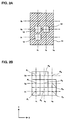
FIG. 14 is a cross-sectional view illustrating a
conventional polyimide/ceramic multilayer wiring board.
-
A ceramic substrate 150 has through holes 151 therein
each which electrically connects with an IO terminal 156.
Wiring layers are formed on the surface of the ceramic
substrate 150. Plural polyimide resin layers 152, each in
which a power-source via hole 112 is formed, are build-up
on the ceramic substrate 150.
-
Each polyimide resin layer 152 is made by repeating a
series of steps including a polyimide-resin-layer forming
step and a wiring layer forming step. The polyimide-resin-layer
forming step includes the steps of coating a
polyimide precursor on the ceramic substrate 150 drying
it, and then forming a power-source via hole 112 in the
coated film. The wiring layer forming step includes a
photolithographic process, vacuum deposition, and plating.
-
In such a layer structure, each of the 1aM layer, the
2aM layer, the 4aM layer, the 5aM layer, and the 7aM layer
acts as a signal layer. Each of the 0aM layer, the 3aM
layer, and the 6aM layer acts as the grounding layer. The
8aM layer acts as a cover surface layer. A power-source
conductive pattern 100a with power-source via holes 112 is
formed on each of the 8aM layer, the 7aM layer, the 4am
layer, and the 1aM. Similarly, a power-source conductive
pattern 100b is formed on each of the 6aM layer, the 3aM
layer, and the 0aM layer. A power-source conductive
pattern 100c is formed on each of the 5aM layer and the
2aM layer.
-
In order to energize the LSI 155 assembled on the upper
surface of the polyimide/ceramic multilayer wiring board
with the above-mentioned structure, the power is first
guided from the IO terminal 156 formed on the back surface
of the ceramic substrate 150 to the 0aM layer through via
holes. Moreover, the power is supplied to the soldering
bump 154 through the 0aM layer and through the power-source
via hole 112 of each layer and through the pad 188
on the 8aM layer being a cover surface layer.
-
Another mounting pad (not shown) is electrically
connected with another soldering bump of the LSI 155 so
that the power is electrically connected to the signal
layer and the ground layer.
-
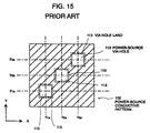
FIG. 15 illustrates a copper-foiled power-source
conductor pattern with power-source via holes, arranged on
the polyimide/ceramic multilayer wiring board shown in FIG.
14. Power-source via holes 112 are respectively formed at
three points of nine points where line segments X1a, X2a
and X3a dividing in the X direction of the power-source
conductor pattern cross with line segments Y1a, Y2a and Y3a
dividing in the Y-direction thereof. The power-source
conductive pattern 100 is of the so-called 3 × 3 matrix
type. Bach power-source conductive pattern 112 is formed
within the via hole land 113 through a photolithographic
process.
-
The power-source conductive pattern 100 has, for example,
a square of 189 (µm) × 189 (µ um). The via hole land 113
has a square of 56 (µm) X 56 (µm). The power-source via
hole 112 has rounded corners R and is of a square of 45
(µm) × 45(µ um).
-
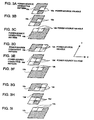
FIGs. 16A to 16I illustrate power-source conductive
patterns arranged on each of laminated layers in the
polyimide/ceramic multilayer wiring board shown in FIG. 11.
That is, FIG. 16I shows the bottom layer. FIG. 16A shows
the top layer. The power-source conductive patterns 100a.
100b, and 100c as well as via holes 112a, 112b and 112c
respectively therein are represented schematically.
-
FIG. 16A shows the power-source conductive pattern 100a
formed on the 8aM layer covering the surface of the top
layer. FIG. 16B shows the power-source conductive pattern
100a arranged on the 7aM layer on which a signal line is
formed in the Y-direction. FIG. 16E shows the power-source
conductive pattern 100a arranged on the 4aM layer on which
a signal line is formed in the Y-direction. FIG. 16H shows
the power-source conductive pattern 100a arranged on the
1aM layer on which a signal line is formed in the Y-direction.
-
FIG. 16C shows the power-source conductive pattern 100b
arranged on the 6aM layer or the ground layer connected to
the ground. FIG. 16F shows the power-source conductive
pattern 100b arranged on the 3aM layer or the ground layer
connected to the ground. FIG. 16I shows the power-source
conductive pattern 100b arranged on the 0aM layer or the
ground layer connected to the ground.
-
Moreover, FIG. 16D shows the power-source conductive
pattern 100c arranged on the 5aM layer on which a signal
line is formed in the X-direction. FIG. 16G shows the
power-source conductive pattern 100c arranged on the 2aM
layer on which a signal line is formed in the X-direction.
-
Each of FIGs. 17A and 17C is a plan view schematically
illustrating a conductive pattern formed on each layer.
-
FIG. 17A shows the power-source pattern 100a arranged on
the layer on which a signal line is formed in the Y-direction.
FIG. 17B shows the power-source pattern 100b
arranged on the layer connected to the ground. FIG. 17C
shows the power-source pattern 100c arranged on the layer
on which the signal line formed in the Y-direction. Three
power-source via holes 112a are arranged in the power-source
conductive pattern 100a, as shown in FIG. 17A.
Three power-source via holes 112b are arranged in the
power-source conductive pattern 100b, as shown in FIG. 17B.
Three power-source via holes 112c are arranged in the
power-source conductive pattern 100c, as shown in FIG. 17C.
That is, the power-source via holes 112a to 112c are
positioned in such a way that the projected positions of
the power-source via holes 112a to 112c are not aligned
with each other when the power-source conductive patterns
100a to 100c are piled up.
-
The power-source conductive patterns 100a to 100c are
piled up in the order shown in FIGs. 16A to 16I. The
power-source via holes 112a to 112c respectively formed in
the power-source conductive patterns 100a to 100c are of
the same type of conductive pattern. For example, the
power-source via hole 112a in the power-source conductive
pattern 100a disposed on a layer having signal lines
formed in the Y-direction is electrically connected to
only the power-source via hole 112a in the power-source
conductive pattern 100a disposed on another layer. In
other type of conductive pattern, that is, both the power-source
via hole 112b formed on the power-source conductive
pattern 100b and the power-source via hole 112c formed on
the power-source conductive pattern 100c are not
electrically connected to the power-source via hole 112a
in the power-source conductive pattern 100a because the
power-source via hole 112a is arranged as shown in the
above example.
-
FIG. 18 illustrates the relationship between conductive
patterns formed on the 5aM layer and X-directional signal
lines.
-
Of areas where five wiring channels can be arranged on
the 5aM layer with the power-source conductive patterns
100c, only the areas where two outer signal lines, that is,
the X-directional signal lines 120 and 121 act as wiring
channels. Three inner signal lines act as non wiring
channels because of the presence of the power-source
conductive pattern 100c.
-
The power-source via holes 112a to 112c are positioned
in such a way that the projection positions thereof are
not aligned with each other in the adjacent layer and the
next adjacent layer. For example, the power-source via
hole 112c on the 2aM layer is formed at a different
position with respect to the power-source via hole 112a on
the 1M layer (an adjacent layer), the power-source via
hole 112b on the 3M layer (an adjacent layer), the power-source
via hole 112a on the 0aM layer (the next adjacent
layer), and the power-source via hole 112a on the 4M layer
(the next adjacent layer). The reason is to solve the
question that degradation of the stiffness of the portion
where upper and lower via holes are aligned with each
other may cause a warp of the polyimide resin layer 152,
so that the reliability of via hole connection cannot be
ensured.
-
Next, a conventional build-up board will be explained
below as one example of multilayer wiring boards.
-
The build-up board belongs to one of multilayer wiring
boards. An insulating layer of a photo-sensitive resin is
formed on a multilayer printed wiring substrate using a
glass epoxy resin insulator. Minute via holes are opened
in the printed substrate using a photolithographic process
or laser. Connection between the upper layer and the lower
layer and pattern formation are performed through a
plating step. Thus, the build-up board is made by
sequentially piling up build-up layers. This allows LSI
terminals to be arranged in high density.
-
FIG. 19 is a plan view schematically and partially
illustrating a conventional build-up board.
-
The mounting pad 188b, on which a soldering bump of a
LSI (not shown) is placed, is electrically connected to a
signal transmission via hole 189 for signal transmission
formed within a via hole land 190. The mounting pad 188a
is electrically connected to a signal transmission via
hole 187b formed within a via hole land 190.
-
The via hole land 190 has a dimension of 0.075 (mm) ×
0.075 (mm). The signal via hole 189 has a diameter of 0.05
mm. The power-source via hole 187b has a diameter of 0.05
mm. The build-up board has a ground via hole (not shown)
of a diameter of 0.05 mm and a via hole land (not shown)
of a diameter of 0.05 mm.
-
However, in order to deal with an increased number of
signals connected between LSIs with the recent trend
toward high density, it is required to increase the number
of wiring channels per layer within a limited number of
wiring layers. The number of via holes for power supplying
or grounding has to be reduced as small as possible.
Meanwhile, the voltage necessary for operation of an LSI
has to be maintained, with an electric resistance
suppressed between the power supply pin on the back
surface of the base substrate and the LSI. This leads to
increasing the diameter of a via hole or to increasing the
number of via holes for power supplying and for grounding
as degree as possible. There is a contradiction between
that approach and a demand for increasing the number of
wiring channels.
-
In the conventional structure, a plurality of via holes
are uniformly arranged in a matrix form of 3 × 3 to one
power supply pin of an LSI, independently of the layer
structure. In the 3 × 3 type arrangement as shown
schematically in FIG. 18, the case often occurs where, of
areas where five wiring channels are disposed, only two
outer lines are wiring channels while the inner three
power-source lines are wiring channels because of the
presence of the power-source conductor pattern 100c. In
the case of the 3 × 3 conductive pattern, since an
increasing number of LSI pins leads to increasing not only
signal lines but also power supply terminals, the number
of signals to be wired increases. However, in that case,
it becomes difficult to increase the number of wiring
channels because of the presence of a conductive pattern
in which via holes are formed. The number of wiring
channels may be increased by densely making the wiring
grid or increasing the number of wiring layers. However,
this approach results in increased costs due to
degradation in product quality.
-
In order to fully power-supply or ground LSIs on the
build-up board, a single power-source via hole or
grounding via hole having the same diameter as that the
signal via hole formed one via hole land has a high
resistance, so that an necessary voltage cannot be often
supplied. In order to decrease the resistance, it is
necessary to increase the size of a via hole. However,
formation of a through hole in the build-up layer makes it
difficult to deal with a high dense assembly being the
feature of the build-up board.
-
The objective of the invention is to provide a
multilayer wiring board that can increase wiring channels
in a wiring layer and can secure power-source via holes
needed for power supplying.
-
A second object of the invention is to provide a
multilayer wiring board that has via holes for power-supplying
and grounding, each having a decreased electric
resistance.
-
In achieve the above mentioned objectives, a multilayer
wiring board according to the present invention comprises
a first wiring layer having a first wiring pattern; a
second wiring layer having a second wiring pattern; the
wiring direction of the first wiring pattern and the
wiring direction of the second wiring pattern being
substantially perpendicularly to each other, the first
wiring layer and second wiring layer being laminated; and
a plurality of conductive patterns formed on each of the
first and second wiring layers in such a way that each of
long sides is oriented substantially in the same direction
as the wiring direction of a wiring pattern formed on each
wiring layer, each of the conductive patterns in which a
plurality of via boles are formed, each of the conductive
patterns having a nearly rectangular form.
-
In the multilayer wiring board with the above-mentioned
structure according to the present invention, the long
side of a rectangular conductive pattern on which via
holes are formed is oriented substantially in the same
direction as that of the wiring pattern. The area occupied
by a wiring pattern in the arranged direction on a
conductive pattern on which the long side is oriented
substantially the same direction as the direction of the
wiring pattern is small, compared with the occupied area
of a conventional rectangular conductive pattern.
-
The position at which each via hole in each of the
conductive patterns formed on the first wiring layer is
projected may not aligned with a position at which each
via hole in each of the conductive patterns formed on the
second wiring layer. This structure can avoid electrically
interconnecting wiring layers on which wiring patterns are
formed in different directions.
-
Moreover, the long side of each of the conductive
patterns may correspond to the length along which at least
three via holes can be formed. The short side of each of
the conductive patterns may correspond to the length along
which at least two via holes can be formed. In this case,
at least two via holes may be formed in each of the
conductive patterns.
-
Moreover, according to the present invention, the
multilayer wiring board comprises a first wiring layer and
a second wiring layer laminated to each other; a plurality
of first conductive patterns arranged on the first wiring
layer, each of the plurality of first conductive patterns
having a plurality of power-source via holes; and a
plurality of second conductive patterns arranged on the
second wiring layer, each of the plurality of second
conductive patterns having a plurality of power-source via
holes at positions which are not aligned with positions
where the via holes in the first pattern are projected.
-
In the multilayer wiring board with the above-mentioned
structure according to the present invention, plural
power-source via holes are formed in the conductive
pattern, so that the electric resistance upon power
supplying can be reduced.
-
Furthermore, according to the present invention, the
multilayer wiring board comprises a first wiring layer and
a second wiring layer laminated to each other; a plurality
of first conductive patterns arranged on the first wiring
layer, each of the plurality of first conductive patterns
having a plurality of grounding via holes; and a plurality
of second conductive patterns arranged on the second
wiring layer, each of the plurality of second conductive
patterns having a plurality of grounding via holes at
positions which are not aligned with positions where the
via holes in the first pattern are projected.
-
In the multilayer wiring board with the above-mentioned
structure according to the present invention, plural
grounding via holes are formed in the conductive pattern,
so that the electric resistance upon power supplying can
be reduced.
-
This and other objects, features and advantages of the
present invention will become more apparent upon a reading
of the following detailed description and drawings, in
which:
- FIG. 1A and FIG. 1B are cross-sectional views
schematically illustrating a polyimide/ceramic multilayer
wiring board according to a first embodiment of the
present invention;
- FIG. 2A and FIG. 2B are plan views illustrating a power-source
conductive pattern according to the first
embodiment of the present invention, indicating the
positions of via holes;
- FIG. 3A to FIG. 3I are schematic diagrams illustrating
power-source conductive patterns respectively arranged on
layers of the polyimide/ceramic multilayer wiring board in
FIG. 1A and 1B;
- FIG. 4A to FIG. 4D are plan views of schematically
illustrating the positions of via holes formed in a power-source
conductive pattern arranged on each layer;
- FIG. 5 is a transparent plan view schematically
illustrating a power-source conductive pattern arranged on
each layer;
- FIG. 6 is a schematic diagram explaining a relationship
between a power-source conductive pattern and a signal
line in the X-direction, which are formed on the 5M layer;
- FIG. 7 is a cross-sectional view schematically
illustrating a build-up board according to a second
embodiment of the invention;
- FIG. 8 is a plan view schematically illustrating the
build-up board shown in FIG. 7;
- FIG. 9A end FIG. 9B are plan views schematically
illustrating the power-source conductive pattern shown in
FIG. 8;
- FIG. 10A and FIG. 10B are diagrams schematically
illustrating the power-source conductive pattern arranged
on each build-up layer;
- FIG. 11 is a diagram explaining dimensions of various
portions of a power-source conductive pattern formed on a
polyimide/ceramic multilayer wiring board according to the
first embodiment of the present invention;
- FIG. 12A and FIG. 12B are diagrams explaining dimensions
of a mounting pad and dimensions of a power-source
conductive pattern, the mounting pad and the power-source
conductive pattern being formed on a build-up layer
according to the second embodiment of the present
invention;
- FIG. 13 is a diagram illustrating the spacing between
mounting pads arranged on a build-up layer according to
the second embodiment of the present invention;
- FIG. 14 is a cross-sectional view schematically
illustrating a conventional polyimide/ceramic multilayer
wiring board;
- FIG. 15 is a plan view illustrating a conventional
power-source conductive pattern;
- FIG. 16A to FIG. 16I are schematic diagrams illustrating
a power-source conductive pattern arranged on each layer
of the polyimide/ceramic cmultilayer wiring board shown in
FIG. 14.
- FIG. 17A to FIG. 17c are cross-sectionals explaining the
positions of via holes formed on the conventional
conductive pattern.
- FIG. 18 is a schematic diagram explaining a relationship
between a power-source conductive pattern and a X-directional
signal line formed on the layer 5aM and
- FIG. 19 is a plan view schematically illustrating a
conventional power-source conductive pattern.
-
-
Embodiments of the present invention will be described
below with reference to the attached drawings.
(First Embodiment)
-
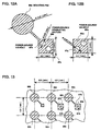
FIG. 1A is a plan view illustrating a polyimide/ceramic
multilayer wiring board according to a first embodiment
of the present invention. FIG. 1B is a cross-sectional
view schematically illustrating the polyimide/ceramic
multilayer wiring board taken along the line A-A of FIG.
1A.
-
Referring to FIG. 1A, mounting pads 8a and 8b, a
rectangular power-source conductive pattern 10, and a
signal via hole 13 are formed on the surface of the
polyimide/ceramic multilayer wiring board. A soldering
bumps 86 of a LSI 55 (to be described later) are
respectively placed on the mounting pads 8a and 8b. The
rectangular power-source conductive pattern 10 is
electrically connected to a mounting pad 8a and has two
power-source via holes 12. The signal via hole 13 is
electrically connected to a mounting pad 8b.
-
Next, the laminated structure of the polyimide/ceramic
multilayer wiring board of the present embodiment will be
explained by referring to FIG. 1B.
-
A plurality of polyimide resin layers 52 are piled up on
the ceramic substrate 50 through which through holes 51
are formed to communicate with IO terminals 56. Each
polyimide resin layer 52 has a wiring layer 0M, .., or 8M
formed on the surface thereof and a power-source via hole
12 to electrically connect to other wiring layer.
-
The method of forming polyimide resin layers 52 includes
the steps of coating a polyimide precursor varnish on the
ceramic substrate 50 (or on the wiring layer of the second
layer or more), drying it, forming on the coated film a
polyimide resin layer in which via holes are to be formed,
forming wiring layers through a photolithographic process,
vacuum deposition, and plating process. A laminated
structure of polyimide resin layers 52, each on which
wiring layers is formed, are fabricated by repeating a
series of the above steps.
-
Each of the wiring layers 1M, 2M, 4M, 5M, and 7M acts as
a signal layer. Each of the wiring layers 0M, 3M, and 6M
acts as a ground layer. The wiring layer 8M acts as a
covered surface layer.
-
Signal layers on which signal lines are arranged in the
Y-direction (in the inner direction in FIG. 1B) correspond
to 1M, 4M and 7M. Signal layers on which signal lines are
arranged in the X-direction (in the horizontal direction
in FIG 1B) correspond to 2M and 5M.
-
In order to energize the LSI 55 assembled on the upper
surface of the polyimide/ceramic multilayer wiring board
with the above structure, the power is first applied from
IO terminal 56 disposed on the back surface of the ceramic
substrate 50 to the 0M layer via a through hole. Moreover,
the power is supplied from the 0M layer to the LSI 55
through the power-source via holes 12 of each layer, the
mounting pad 8a formed on the cover surface layer or 8M
layer, end the soldering bump 54.
-
The soldering bump 86 of the LSI 55 is electrically
connected to the mounting pad 8b, thus being connected to
the signal layer.
-
FIG. 2A is a plan view illustrating a copper-foiled
power-source conductive pattern which is disposed on the
1M or 4M layer of the polyimide/ceramic multilayer wiring
board shown in FIG. 1B and which has power-source via
holes formed therein. Each power-source via hole 12 is
formed at each of three points of six points where line
segments X1 and X2 dividing in the X direction of the
rectangular power-source conductor pattern 10a cross with
line segments Y1, Y2 and Y3 dividing in the Y-direction
thereof. The power-source via hole 12 is formed using the
photolithographic process.
-
FIG. 2B is a schematic diagram explaining the positions
of power-source via holes 12a, 12a', 12b, and 12c (to be
described later). Referring to FIGs. 3 to 6, the positions
of the power-source via holes 12a, 12a', 12b, and 12c are
schematically shown.
-
The line segments X1, X2 and X3 and the line segments Y1,
Y2 and Y3 shown in FIG. 2B correspond to those in FIG. 2A,
respectively. P1 to P9 respectively represent cross points
between the line segments. Areas surrounded by solid lines
in FIG. 2B represent power-source via holes 12a, 12a', 12b,
and 12c. For example, three power-source via holes 12 in
FIG. 2A are formed at the positions p1, P4 and p5 shown in
FIG. 2B, respectively. Explanation will be made referring
to the positions P1 to P9 of via holes. In the embodiment.
a via hole is not formed at the position P9. However, the
present invention should not be limited to only this
embodiment. If necessary, a via hole may be formed at the
position P9.
-
Next, referring to FIGs. 3A to 3I, power-source
conductive patterns to be respectively formed on the
wiring layers 0M to 8M in the polyimide/ceramic multilayer
wiring board shown in FIG. 1 are shown in the order of
laminated layers. That is, FIG. 3I shows the lowest layer,
or the 0M layer. FIG. 3A shows the top layer, or, the 8M
layer.
-
FIG. 3A shows the power-source conductive pattern 10a
formed on the 8M layer and covering the top surface. FIG.
3B shows the power-source conductive pattern 10a on the 7M
layer on which signal lines are arranged in the Y-direction.
-
FIG. 3E shows the 4M layer on which signal lines are
arranged in the Y-direction, as shown with the 7M layer.
FIG. 3H shows the power-source conductive pattern 10a' on
the 1M layer.
-
FIG. 3C shows the power-source conductive pattern 10b
formed on the 6M layer being the ground layer. FIG. 3F
shows the power-source conductive pattern 10b formed on
the 3M layer being the ground layer. FIG. 3I shows the
power-source conductive pattern 10b formed on the 0M layer
being the ground layer.
-
Moreover, FIG. 3D shows the power-source conductive
pattern 10c on the 5M layer on which signal lines are
arranged in the X-direction. FIG. 3G shows the power-source
conductive pattern 10c on the 2M layer on which
signal lines are arranged in the X-direction.
-
Next, FIGs. 4A to 4D are plan views each schematically
illustrating a power-source conductive pattern on each
layer.
-
FIG. 4A shows the conductive pattern 10a formed on the
8M layer and the 7M layer. FIG. 4B shows the conductive
pattern 10a' formed on the 4M layer and the 1M layer. FIG.
4C shows the conductive pattern 10c formed on the 6M layer,
the 3M layer and the 0M layer. FIG. 4D shows the power-source
conductive pattern 10d formed on the 5M layer and
the 2M layer.
-
In the power-source conductive pattern 10a in FIG. 4A,
the power-source via holes 12a are respectively formed at
the positions P1 and P5. In the power-source conductive
pattern 10a' in FIG. 4B, the power-source via holes 12a'
are respectively formed at the positions P1, P4, and P5. In
the power-source conductive pattern 10b in FIG. 4C, the
power-source via boles 12b are respectively formed at the
positions P7 and P8. In the power-source conductive
pattern 10c in FIG. 4D, the power-source via holes 12c'
are respectively formed at the positions P2 P3 and P6.
-
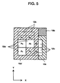
FIG. 5 is a transparent plan view schematically
illustrating relationships between projected positions of
a power-source via hole formed in the power-source
conductive pattern on a layer on which signal lines are
arranged in the Y-direction and a power-source via hole
formed in the power-source conductive pattern on a layer
on which signal lines are arranged in the X-direction and
a power-source via hole formed in the power-source
conductive pattern of the ground layer, in a laminated
state.
-
As shown in Fig. 5, among the power-source via hole 12a'
formed at the positions P1, P4 and P5 of a power-source
conductive pattern 10a', the power-source via hole 12c
formed at the positions P2, P3 and P6 of a power-source
conductive pattern 10c and the power-source via hole 12b
formed at the positions P7 and P8 of a power-source
conductive pattern 10b, the projected positions thereof
are not overlapped.
-
In other words, the power-source conductive patterns
10a', 10b and 10c are piled up in the order shown in FIGs.
3A to 3I. Of the power-source via hole 12a' formed in the
power-source conductive pattern 10a', the power-source via
hole 12b formed in the power-source conductive pattern 10b,
and the power-source via hole 12c formed in the power-source
conductive pattern 10c, the same patterns are
electrically connected together. For example, the power-source
via holes 12a', which are formed at the positions
P1, P4 and P5 of the power-source conductive pattern 10a'
on the 1M layer on which signal lines are arranged in the
Y-direction, are connected respectively and electrically
with the power-source via holes 10a', which are formed at
the positions P1, P4 and P5 of the power-source conductive
pattern 10a' on the 5M layer on which signal lines are
arranged in the Y-direction. The power-source via holes
12a, which are formed at the positions P1 and P5 of the
power-source conductive pattern 10a on the 7M layer on
which signal lines are arranged in the Y-direction, are
connected respectively and electrically with the power-source
via holes 12a', which are formed at the positions
P1 and P5 of the power-source conductive pattern 10a' on
each of the 1M and 5M layers. In other type of pattern,
the power-source via holes 12b formed in the power-source
conductive pattern 10b and the power-source via holes 12c
formed in the power-source conductive pattern 10c are
formed at positions other than the positions P1, P4 and P5.
Hence, the power-source via hole 12a' in the power-source
conductive pattern 10a' is not electrically connected with
the power-source via hole 12a in the power-source
conductive pattern 10a.
-
Except for the relationship between the 8M layer being a
cover surface layer and the 7M layer being the layer
underneath the 8M layer, respective layers are piled up in
such a way that the power-source via holes 12a', 12b and
12c are not projected on an adjacent layer and the next
adjacent layer. For example, as shown in FIG. 3, the
power-source via holes 12c in the 2M layer (FIG. 3G) is
disposed at a position different from the positions of the
power-source via holes 12a' in the 1M layer (adjacent
layer) (FIG. 3H), the power-source via holes 12b in the 3M
layer (FIG. 3F), the the power-source via holes 10b in the 0M
layer (the next adjacent layer) (FIG. 3I), and the power-source
via holes 10a' in the 4M layer (FIG. 3E). That is,
the same patterns (including the power-source conductive
pattern 10c on the 2M layer and the power-source
conductive pattern 10c on the 5M layer) are piled up while
two different patterns (including the power-source
conductive pattern 10b on the 3M layer and the power-source
conductive pattern 10a' on the 4M layer) are piled
up. When the via hole in the upper layer and is aligned
with the via hole in the lower layer, the rigidity of the
polyimide resin layer 152 is degraded at the overlapped
portion. This may cause a warp, or deformation, of the
polyimide resin layer 152. The above structure can prevent
the reliability in connection between via holes from being
degraded.
-
FIG. 6 is a diagram schematically illustrating a
relationship between power-source conductive patterns and
signal lines arranged in the X-direction on the 5M layer.
-
Since the conventional power-source conductive pattern
100c shown in FIG. 18 has a 3 × 3 matrix form, it exists
even in the area (shown with broken lines).
-
According to the present embodiment, since the long side
of the power-source conductive pattern 10c is arranged in
the same direction of as that of signal lines, the power-source
conductive pattern 10c exists in only the area
(shown with solid lines). The area shown with broken lines
becomes an extra area. This makes it possible to arrange
not only the signal lines 20 and 21 in the X-direction of
five wiring channels but also the signal line 22 in the X-direction.
That is, the number of wiring channels can be
increased from two to three. Similarly, the number of
wiring channels in the X-directional signal line on the 2M
layer can be increased by one. As to the 7M layer, the 4M
layer and the 1M layer, the number of wiring channels in
the Y-directional signal line can be increased by one,
compared with the conventional power-source conductive
pattern 100a.
-
As described above, the present embodiment can increase
the number of wiring channels since a power-source
conductive pattern is arranged between wiring patterns so
as to the long side of the power-source conductive pattern
is oriented in the same direction as that of the wiring
patterns.
(Second Embodiment)
-
FIG. 7 is a cross-sectional view partially illustrating
a build-up board on which a LSI is mounted on the surface
thereof, according to the second embodiment of the present
invention. FIG. 8 is a plan view schematically and
partially illustrating the build-up board shown in FIG. 7.
FIG. 7 is a side cross-sectional view illustrating the
build-up board taken along the line B-B in FIG. 8.
-
Build-up layers 82a and 82b are build-up over a
multilayer printed wiring board 80. The multilayer printed
wiring board 80, using a glass epoxy resin acting as an
insulator, has through via 81 therein. The build-up layer
82a has a power-source via hole 87a while the build-up
layer 82b has a power-source via hole 87b. Mounting pads
88a, each on which a soldering bump 86 of the LSI 85 is
placed, are formed on the surface of the build-up layer
82b. A power-source via hole 87a and a signal via hole 89a,
each having a minute diameter, are opened in the build-up
layer 82a using the photolithographic process or laser
beam. Thereafter, electrical connections with the top
surface of the multilayer printed wiring board 80 as well
as patterning are performed through plating while the
build-up layer 82a is build-up on the multilayer printed
wiring board 80. Next, a power-source via hole 87b is
opened in the build-up layer 82b. Thereafter, electrical
connections with the build-up layer 82a as well as
patterning are performed through plating while the build-up
layer 82b is build-up on the build-up layer 82a.
-
Thus, the soldering bumps 86 of the LSI 85 are
respectively placed on the mounting pads 86a of the build-up
layer 82b of the resultant build-up board so that the
LSI 85 is electrically connected with the build-up board.
-
Round mounting pads 86a and 86b are arranged at equal
intervals, as shown in FIG. 8. The mounting pad 86a is
electrically connected to two power-source via holes 87b
for power supplying, which are formed on the square power-source
conductive pattern 90b. The mounting pad 88b is
electrically connected to the signal via hole 89 for
signal transmission.
-
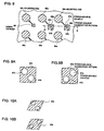
FIG. 9A is a plan view schematically illustrating the
locations of power-source via holes opened in a power-source
conductive pattern on the build-up layer. FIG. 9B
is a plan view schematically illustrating the locations of
power-source via holes opened in a power-source conductive
pattern on the build-up layer. FIG. 10A is a perspective
view schematically illustrating a power-source conductive
pattern. FIG. 10B is a perspective view schematically
illustrating a power-source conductive pattern.
-
Two power-source via holes 87a formed in the power-source
conductive pattern 90b as well as two power-source
via holes 87a formed in the power-source conductive
pattern 90a are positioned so as not to be electrically
connected to each other.
-
Two power-source via holes 87b are formed in the power-source
conductive pattern 90b on the build-up layer 82b.
This enables halving the electric resistance, compared
with the single power-source via hole 187b formed in the
via hole land 190 shown in FIG. 19.
-
Since the power-source via hole 87a and the power-source
via hole 87b are positioned so as not to be connected to
each other electrically, any communication between the
power supply route for the build-up layer 82a and the
power supply route for the build-up layer 82b does not
achieved.
-
This embodiment employs round power-source via holes 87a
and 87b. However, rectangular power-source via holes may
be used, without being restricted to only the embodiment.
-
Moreover, the present embodiment employs the power-source
via holes 87a and 87b end conductive patterns 90a
and 90b. However, the ground via holes grounded and
conductive patterns grounded may have a similar structure.
-
As described above, according to the present embodiment,
an increased number of via holes for power supplying and
grounding leads to reducing the electric resistance of a
via hole.
-
First and second concrete embodiments are shown below.
However, it should be noted that the present invention is
not limited to these embodiments.
(First Embodiment)
-
The first embodiment of the present invention will be
first described below. FIG. 11 shows dimensions of a
power-source conductive pattern and dimensions of a power-source
via hole and dimensions of a via hole land, in the
present embodiment.
-
The power-source conductive pattern 210 has a
rectangular form of 189 (µm) × 124 (µm). The via hole
land 213 has a square form of 56 (µm) × 56 (µm). The
power-source via hole 212 has rounded corners R and is of
a square form of 45 (µm) × 45 (µm).
-
In the present embodiment, the polyimide/ceramic
multilayer wiring board has an area of 225 (mm2) and
carries 7 × 6 LSIs each of which each side has 25 power
supply terminals.
-
Since 25 power-source conductive patterns 210 are formed
corresponding to 25 power-source conductive patterns 210
of the LSI, the number of wiring channels is increased by
25. This means that the line length of 35 (m) per signal
layer is increased so that the effective wiring length is
increased about 8 (%).
(Second Embodiment)
-
Next, the second embodiment of the present invention
will be described below.
-
The present embodiment uses the build-up board shown in
FIGs. 7 and 8. Like numerals are attached to the same
constituent elements as those shown in FIGs. 7 and 8.
-
FIG. 12A shows the dimensions of a mounting pad and the
dimensions of a power-source conductive pattern, formed on
the build-up layer. FIG. 12B shows the dimensions of a
power-source conductive pattern formed on the build-up
layer
-
The mounting pad has a diameter of 0.25 (mm). The power-source
conductive pattern 90b has a square form of 0.2 ×
0.2 (mm). Two power-source via holes 87b of a diameter of
0.05 (mm) are respectively formed on the upper left and
the lower right within the power-source conductive pattern
90b. The power-source via hole 87a of a diameter of 0.05
(mm) is formed on the upper right and the lower left
within the power-source conductive pattern 90a.
-
FIG. 13 shows the spacing between mounting pads arranged
on a build-up layer. The mounting pads 88a and 88b are
arranged at intervals of 0.5 (mm).
-
According to the present embodiment, the power-source
via holes 87a and 87b are formed so as not to be aligned
with each other at the projection position. Hence, the
power supply route for the build-up layer 82a and the
build-up layer 82b can be provided differently. Moreover,
two power-source via holes 87a are formed in a power-source
conductive pattern while two power-source via holes
87b are formed in a power-source conductive pattern. This
arrangement enables the electric resistance to be reduced,
compared with the power-source via hole 187b shown in FIG.
19.
-
As described above, according to the multiple wiring
board according to the present invention, the rectangular
conductive pattern with via holes is arranged between
wiring patterns while the long side thereof is oriented
substantially in the direction of the wiring patterns. For
that reason, the area occupied by each conductive pattern
in the arrangement direction of wiring patterns is small.
compared with the area occupied by the conventional square
conductive pattern. The extra areas, not occupied by the
conductive patterns and via holes can be utilized as
wiring-pattern forming areas, thus resulting in an
increased number of wiring channels.
-
Moreover, the increased number of via holes for power
supplying and grounding can reduce the electric resistance
of the via hole.