EP0620589A1 - Leadframe structure for molded package arrangements - Google Patents
Leadframe structure for molded package arrangements Download PDFInfo
- Publication number
- EP0620589A1 EP0620589A1 EP94302067A EP94302067A EP0620589A1 EP 0620589 A1 EP0620589 A1 EP 0620589A1 EP 94302067 A EP94302067 A EP 94302067A EP 94302067 A EP94302067 A EP 94302067A EP 0620589 A1 EP0620589 A1 EP 0620589A1
- Authority
- EP
- European Patent Office
- Prior art keywords
- wirebond
- leadframe
- molding
- protective layer
- sites
- Prior art date
- Legal status (The legal status is an assumption and is not a legal conclusion. Google has not performed a legal analysis and makes no representation as to the accuracy of the status listed.)
- Withdrawn
Links
- 239000000463 material Substances 0.000 claims abstract description 18
- 238000000465 moulding Methods 0.000 claims abstract description 17
- RYGMFSIKBFXOCR-UHFFFAOYSA-N Copper Chemical compound [Cu] RYGMFSIKBFXOCR-UHFFFAOYSA-N 0.000 claims description 10
- 229910052802 copper Inorganic materials 0.000 claims description 10
- 239000010949 copper Substances 0.000 claims description 10
- PCHJSUWPFVWCPO-UHFFFAOYSA-N gold Chemical compound [Au] PCHJSUWPFVWCPO-UHFFFAOYSA-N 0.000 claims description 9
- 229910052737 gold Inorganic materials 0.000 claims description 9
- 239000010931 gold Substances 0.000 claims description 9
- 230000001681 protective effect Effects 0.000 claims description 9
- 239000011241 protective layer Substances 0.000 abstract description 12
- 238000000034 method Methods 0.000 abstract description 8
- 239000012778 molding material Substances 0.000 abstract description 4
- 238000007747 plating Methods 0.000 abstract description 2
- 239000010410 layer Substances 0.000 description 9
- 229920005989 resin Polymers 0.000 description 8
- 239000011347 resin Substances 0.000 description 8
- PXHVJJICTQNCMI-UHFFFAOYSA-N Nickel Chemical compound [Ni] PXHVJJICTQNCMI-UHFFFAOYSA-N 0.000 description 6
- 238000004806 packaging method and process Methods 0.000 description 4
- 239000011248 coating agent Substances 0.000 description 3
- 238000000576 coating method Methods 0.000 description 3
- 229910052759 nickel Inorganic materials 0.000 description 3
- VHUUQVKOLVNVRT-UHFFFAOYSA-N Ammonium hydroxide Chemical compound [NH4+].[OH-] VHUUQVKOLVNVRT-UHFFFAOYSA-N 0.000 description 2
- 239000000908 ammonium hydroxide Substances 0.000 description 2
- 230000000740 bleeding effect Effects 0.000 description 2
- 238000004140 cleaning Methods 0.000 description 2
- 150000001875 compounds Chemical class 0.000 description 2
- 230000009977 dual effect Effects 0.000 description 2
- 239000004033 plastic Substances 0.000 description 2
- 229910052709 silver Inorganic materials 0.000 description 2
- 239000004332 silver Substances 0.000 description 2
- 230000002411 adverse Effects 0.000 description 1
- 230000015556 catabolic process Effects 0.000 description 1
- 239000012459 cleaning agent Substances 0.000 description 1
- 238000006731 degradation reaction Methods 0.000 description 1
- 229920006336 epoxy molding compound Polymers 0.000 description 1
- 239000002184 metal Substances 0.000 description 1
- 229910052751 metal Inorganic materials 0.000 description 1
- 238000001465 metallisation Methods 0.000 description 1
- 229920003986 novolac Polymers 0.000 description 1
- 230000005693 optoelectronics Effects 0.000 description 1
- 239000004065 semiconductor Substances 0.000 description 1
- 239000004634 thermosetting polymer Substances 0.000 description 1
Images
Classifications
-
- H—ELECTRICITY
- H01—ELECTRIC ELEMENTS
- H01L—SEMICONDUCTOR DEVICES NOT COVERED BY CLASS H10
- H01L21/00—Processes or apparatus adapted for the manufacture or treatment of semiconductor or solid state devices or of parts thereof
- H01L21/02—Manufacture or treatment of semiconductor devices or of parts thereof
- H01L21/04—Manufacture or treatment of semiconductor devices or of parts thereof the devices having potential barriers, e.g. a PN junction, depletion layer or carrier concentration layer
- H01L21/48—Manufacture or treatment of parts, e.g. containers, prior to assembly of the devices, using processes not provided for in a single one of the groups H01L21/18 - H01L21/326 or H10D48/04 - H10D48/07
- H01L21/4814—Conductive parts
- H01L21/4821—Flat leads, e.g. lead frames with or without insulating supports
- H01L21/4835—Cleaning, e.g. removing of solder
-
- H—ELECTRICITY
- H01—ELECTRIC ELEMENTS
- H01L—SEMICONDUCTOR DEVICES NOT COVERED BY CLASS H10
- H01L23/00—Details of semiconductor or other solid state devices
- H01L23/48—Arrangements for conducting electric current to or from the solid state body in operation, e.g. leads, terminal arrangements ; Selection of materials therefor
- H01L23/488—Arrangements for conducting electric current to or from the solid state body in operation, e.g. leads, terminal arrangements ; Selection of materials therefor consisting of soldered or bonded constructions
- H01L23/495—Lead-frames or other flat leads
-
- H—ELECTRICITY
- H01—ELECTRIC ELEMENTS
- H01L—SEMICONDUCTOR DEVICES NOT COVERED BY CLASS H10
- H01L2924/00—Indexing scheme for arrangements or methods for connecting or disconnecting semiconductor or solid-state bodies as covered by H01L24/00
- H01L2924/0001—Technical content checked by a classifier
- H01L2924/0002—Not covered by any one of groups H01L24/00, H01L24/00 and H01L2224/00
Definitions
- the present invention relates to a leadframe structure and, more particularly, to a leadframe structure useful in molded packaging arrangements.
- one or more semiconductor components are positioned on a leadframe and encased in a package, so as to form a single in-line package (SIP) or dual in-line package (DIP) structure.
- the package may be, in some cases, molded from a plastic to completely encase the circuit components.
- electrical signals are transmitted to/from such a molded package to the associated circuit board by the plurality of leads which comprise the leadframe structure.
- the need arises to provide a direct electrical contact between the molded package and another device without passing through the circuit board (e.g., in situations where the signal degradation associated with the circuit board is unacceptable).
- a problem with the direct wirebond is that an essentially clean wirebond contact on the molded package is required to provide the necessary electrical connections and mechanical integrity.
- inherent in the molding operation is the residue of molding compound (typically, a thermoset resin) which will adhere to the exposed wirebond surface.
- Conventional cleaning agents which may be capable of removing the resin from the exposed gold wirebond pad sites, are not acceptable alternatives since they have been found to attack the molded package and/or gold wirebond contact area, as well as require a one-at-a-time cleaning process (costly as compared to a "batch" cleaning system).
- the present invention relates to a leadframe structure and, more particularly, to a leadframe structure useful in molded packaging arrangements.
- a conventional copper leadframe (prior to the molding operation) is blanket plated with nickel, then selectively plated (in wirebond locations) or blanket plated with gold.
- the gold-plated wirebond areas are subsequently plated with a protective material (for example, copper).
- the structure is then over-molded, using any desired molding process, often resulting in a portion of the molding resin bleeding over into the wirebond sites. After molding, the structure is exposed to an etchant which is selective between nickel and the protective material such that only the protective layer (and resin coating) is removed. Therefore, the underlying leadframe and the virgin gold contact areas of the wirebond sites are exposed.
- copper may be used as the protective material, where an etchant comprising approximately 10% ammonium hydroxide and 10% HCl may be used.
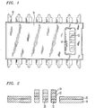
- FIG. 1 illustrates an exemplary molded package 10 which contains wirebond locations 12 which may be subject to being covered by resin during the molding operation.
- wirebond locations 12 which may comprise gold contacts, are visible through a window 14 formed in a molded package 16.
- Molded package 16 may comprise any suitable molding compound commonly used for molding operations, for example, a commercially available epoxy molding compound, such as cresol-novolacs.
- the molding process may result in a certain amount of the molding material, referred to as resin, "bleeding" onto the wirebond locations. Obviously, the coating of resin over the wirebond sites will adversely affect the integrity of any subsequent wirebond attachment.
- the present invention relates to utilizing a leadframe structure wherein the exposed wirebond sites are covered with a protective (i.e., sacrificial) layer prior to the molding process.
- the protective layer is then removed after the molding process, taking with it the resin coating.
- the underlying metal (e.g., gold) wirebond sites are then exposed and may be used to provide robust mechanical and electrical contacts.
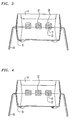
- Leadframe 18 may comprise any suitable material, where in most conventional embodiments, a copper leadframe is used. In the conventional processing of a leadframe, the copper leadframe may also be blanket plated with a nickel layer 20. An intermediate layer of metallization, for example, silver, may be included at this location of the structure. In accordance with the leadframe structure of the present invention, the locations of wirebond sites, denoted 12 in FIG. 2, are further plated with the material 22 to be used to form the bond pads for the wirebond contacts. For example, gold may be used to form plated layer 22. As shown in FIG. 2, a protective layer 24 is formed so as to cover layer 22.
- Protective layer 24 must comprise a material which may later be removed by an etch process, using an etchant which will not affect the rest of the nickel-plated copper leadframe 18, underlying contact layer 22, or plastic packaging. In one embodiment, copper may be used to form protective plating layer 24.
- FIG.3 A cut-away side view of a molded package 16 including a plated leadframe 18 as discussed above is illustrated in FIG.3.
- a residue 26 of the molding material (resin) has coated protective layer 24.
- residue 26 is then removed by using an etchant which will preferentially etch protective layer 24 with respect to the remaining leadframe material.
- an etchant comprising 10% ammonium hydroxide and 10% HCl may be used.
- FIG. 4 contains a cut-away side view of an exemplary molded package after the removal of residue 26 and protective layer 24 with the etchant. As shown, the removal of these layers allows for the contact layer 22 (usually gold) to be exposed and available for wirebond attachments.
- protective layer 24 various other materials (and associated etchants) may be used to form protective layer 24.
- materials for example, silver, may also be used. It is to be understood that many other materials may also be used and are considered to fall within the spirit and scope of the present invention.
Landscapes
- Engineering & Computer Science (AREA)
- Physics & Mathematics (AREA)
- Condensed Matter Physics & Semiconductors (AREA)
- General Physics & Mathematics (AREA)
- Computer Hardware Design (AREA)
- Microelectronics & Electronic Packaging (AREA)
- Power Engineering (AREA)
- Manufacturing & Machinery (AREA)
- Lead Frames For Integrated Circuits (AREA)
Applications Claiming Priority (2)
| Application Number | Priority Date | Filing Date | Title |
|---|---|---|---|
| US4023693A | 1993-03-30 | 1993-03-30 | |
| US40236 | 1993-03-30 |
Publications (1)
| Publication Number | Publication Date |
|---|---|
| EP0620589A1 true EP0620589A1 (en) | 1994-10-19 |
Family
ID=21909897
Family Applications (1)
| Application Number | Title | Priority Date | Filing Date |
|---|---|---|---|
| EP94302067A Withdrawn EP0620589A1 (en) | 1993-03-30 | 1994-03-23 | Leadframe structure for molded package arrangements |
Country Status (4)
Citations (4)
| Publication number | Priority date | Publication date | Assignee | Title |
|---|---|---|---|---|
| JPS6396947A (ja) * | 1986-10-13 | 1988-04-27 | Mitsubishi Electric Corp | 半導体装置用リ−ドフレ−ム |
| EP0354800A2 (en) * | 1988-08-12 | 1990-02-14 | Mitsui Petrochemical Industries, Ltd. | Processes for producing semiconductor devices |
| US4968397A (en) * | 1989-11-27 | 1990-11-06 | Asher Reginald K | Non-cyanide electrode cleaning process |
| JPH0451531A (ja) * | 1990-06-19 | 1992-02-20 | Mitsubishi Electric Corp | 絶縁封止型半導体装置の製造方法 |
-
1993
- 1993-08-13 TW TW082106493A patent/TW256946B/zh active
-
1994
- 1994-03-23 EP EP94302067A patent/EP0620589A1/en not_active Withdrawn
- 1994-03-29 KR KR1019940006324A patent/KR940022819A/ko not_active Withdrawn
- 1994-03-30 JP JP6059626A patent/JPH06310638A/ja not_active Withdrawn
Patent Citations (4)
| Publication number | Priority date | Publication date | Assignee | Title |
|---|---|---|---|---|
| JPS6396947A (ja) * | 1986-10-13 | 1988-04-27 | Mitsubishi Electric Corp | 半導体装置用リ−ドフレ−ム |
| EP0354800A2 (en) * | 1988-08-12 | 1990-02-14 | Mitsui Petrochemical Industries, Ltd. | Processes for producing semiconductor devices |
| US4968397A (en) * | 1989-11-27 | 1990-11-06 | Asher Reginald K | Non-cyanide electrode cleaning process |
| JPH0451531A (ja) * | 1990-06-19 | 1992-02-20 | Mitsubishi Electric Corp | 絶縁封止型半導体装置の製造方法 |
Non-Patent Citations (2)
| Title |
|---|
| PATENT ABSTRACTS OF JAPAN vol. 012, no. 335 (E - 656) 9 September 1988 (1988-09-09) * |
| PATENT ABSTRACTS OF JAPAN vol. 016, no. 246 (E - 1212) 5 June 1992 (1992-06-05) * |
Also Published As
| Publication number | Publication date |
|---|---|
| KR940022819A (ko) | 1994-10-21 |
| JPH06310638A (ja) | 1994-11-04 |
| TW256946B (GUID-C5D7CC26-194C-43D0-91A1-9AE8C70A9BFF.html) | 1995-09-11 |
Similar Documents
| Publication | Publication Date | Title |
|---|---|---|
| US5619068A (en) | Externally bondable overmolded package arrangements | |
| US6194777B1 (en) | Leadframes with selective palladium plating | |
| US10431560B2 (en) | Molded semiconductor package having an optical inspection feature | |
| US5953589A (en) | Ball grid array semiconductor package with solder balls fused on printed circuit board and method for fabricating the same | |
| KR20010052602A (ko) | 반도체 장치용 리드 프레임 | |
| EP0794572A3 (en) | Electronic component, method for making the same, and lead frame and mold assembly for use therein | |
| US5328552A (en) | Leadframe processing for molded package arrangements | |
| US7723163B2 (en) | Method of forming premolded lead frame | |
| US5833758A (en) | Method for cleaning semiconductor wafers to improve dice to substrate solderability | |
| JP3008470B2 (ja) | リードフレーム | |
| EP0620589A1 (en) | Leadframe structure for molded package arrangements | |
| HK1006374A (en) | Leadframe structure for molded package arrangements | |
| US5345038A (en) | Multi-layer ceramic packages | |
| US7504712B2 (en) | Electronic device with selective nickel palladium gold plated leadframe and method of making the same | |
| JP2596542B2 (ja) | リードフレームおよびそれを用いた半導体装置 | |
| JP2977052B2 (ja) | シールド付リードレスパッケージ | |
| JP2813588B2 (ja) | 半導体装置およびその製造方法 | |
| JPH07249707A (ja) | 半導体パッケージ | |
| KR100306230B1 (ko) | 반도체 패키지 구조 | |
| JP2952286B2 (ja) | ベアチップリードレスパッケージ | |
| US20030042594A1 (en) | Semiconductor package and method of manufacturing lead | |
| KR100258603B1 (ko) | 리드프레임을 이용한 에어리어 어레이 범프드 반도체패키지의 입출력 단자용 랜드형성 방법 및 그 구조를 포함하는 반도체 패 키지 | |
| JPS5930535Y2 (ja) | 半導体装置 | |
| JPH02250364A (ja) | リードフレーム及びその製造方法 | |
| KR19980027397A (ko) | 버틈 리드 패키지의 제조방법 |
Legal Events
| Date | Code | Title | Description |
|---|---|---|---|
| PUAI | Public reference made under article 153(3) epc to a published international application that has entered the european phase |
Free format text: ORIGINAL CODE: 0009012 |
|
| AK | Designated contracting states |
Kind code of ref document: A1 Designated state(s): DE ES FR GB IT |
|
| 17P | Request for examination filed |
Effective date: 19950406 |
|
| 17Q | First examination report despatched |
Effective date: 19980520 |
|
| STAA | Information on the status of an ep patent application or granted ep patent |
Free format text: STATUS: THE APPLICATION IS DEEMED TO BE WITHDRAWN |
|
| 18D | Application deemed to be withdrawn |
Effective date: 19981201 |
|
| REG | Reference to a national code |
Ref country code: HK Ref legal event code: WD Ref document number: 1006374 Country of ref document: HK |