EP0620524A2 - Verbesserungen an Speichern und deren Herstellung - Google Patents
Verbesserungen an Speichern und deren Herstellung Download PDFInfo
- Publication number
- EP0620524A2 EP0620524A2 EP94301771A EP94301771A EP0620524A2 EP 0620524 A2 EP0620524 A2 EP 0620524A2 EP 94301771 A EP94301771 A EP 94301771A EP 94301771 A EP94301771 A EP 94301771A EP 0620524 A2 EP0620524 A2 EP 0620524A2
- Authority
- EP
- European Patent Office
- Prior art keywords
- xor
- circuit
- circuits
- block
- output
- Prior art date
- Legal status (The legal status is an assumption and is not a legal conclusion. Google has not performed a legal analysis and makes no representation as to the accuracy of the status listed.)
- Withdrawn
Links
Images





Classifications
-
- G—PHYSICS
- G11—INFORMATION STORAGE
- G11C—STATIC STORES
- G11C29/00—Checking stores for correct operation ; Subsequent repair; Testing stores during standby or offline operation
- G11C29/04—Detection or location of defective memory elements, e.g. cell constructio details, timing of test signals
- G11C29/08—Functional testing, e.g. testing during refresh, power-on self testing [POST] or distributed testing
- G11C29/12—Built-in arrangements for testing, e.g. built-in self testing [BIST] or interconnection details
- G11C29/44—Indication or identification of errors, e.g. for repair
-
- G—PHYSICS
- G06—COMPUTING OR CALCULATING; COUNTING
- G06F—ELECTRIC DIGITAL DATA PROCESSING
- G06F11/00—Error detection; Error correction; Monitoring
- G06F11/07—Responding to the occurrence of a fault, e.g. fault tolerance
- G06F11/08—Error detection or correction by redundancy in data representation, e.g. by using checking codes
- G06F11/10—Adding special bits or symbols to the coded information, e.g. parity check, casting out 9's or 11's
- G06F11/1008—Adding special bits or symbols to the coded information, e.g. parity check, casting out 9's or 11's in individual solid state devices
- G06F11/1012—Adding special bits or symbols to the coded information, e.g. parity check, casting out 9's or 11's in individual solid state devices using codes or arrangements adapted for a specific type of error
-
- G—PHYSICS
- G11—INFORMATION STORAGE
- G11C—STATIC STORES
- G11C29/00—Checking stores for correct operation ; Subsequent repair; Testing stores during standby or offline operation
- G11C29/04—Detection or location of defective memory elements, e.g. cell constructio details, timing of test signals
- G11C29/08—Functional testing, e.g. testing during refresh, power-on self testing [POST] or distributed testing
- G11C29/12—Built-in arrangements for testing, e.g. built-in self testing [BIST] or interconnection details
- G11C2029/4402—Internal storage of test result, quality data, chip identification, repair information
-
- G—PHYSICS
- G11—INFORMATION STORAGE
- G11C—STATIC STORES
- G11C29/00—Checking stores for correct operation ; Subsequent repair; Testing stores during standby or offline operation
- G11C29/70—Masking faults in memories by using spares or by reconfiguring
- G11C29/88—Masking faults in memories by using spares or by reconfiguring with partially good memories
-
- G—PHYSICS
- G11—INFORMATION STORAGE
- G11C—STATIC STORES
- G11C5/00—Details of stores covered by group G11C11/00
- G11C5/02—Disposition of storage elements, e.g. in the form of a matrix array
- G11C5/04—Supports for storage elements, e.g. memory modules; Mounting or fixing of storage elements on such supports
Definitions
- This invention broadly relates to a method and to a circuitry to enable use of partially operative memories, that is memories having faulty locations, as well as to an equipment for mass production of suitable mapped memory blocks and for large scale exploitation of such circuit approach.
- a first aspect of this invention related to focussing a method to utilize semiconductor dynamic memories having manufacturing defects, namely memories having faulty locations and as such not utilizable in conventional applications.
- this invention relates to a circuit approach adapted to exploitation of such a method and, therefore, adapted to detect and to correct errors not detectable or not corrigible by means of approaches according to the prior art.
- this invention relates to an equipment for mapping or practically testing single memory modules and for permanently storing the final map in an OTP (One Time Programmable) memory, in order to enable use of said memory modules in the circuitry and according to the method of this invention.
- OTP One Time Programmable
- the production efficiency of the memory circuits is a monotonically decreasing function of the utilized silicon surface and in effect of the number of memory cells utilized on a single chip.
- this invention is based upon the concept of developing a memory array adapted to operate by blocks and then of retrieving memory blocks, rather than memory bytes, thereby renouncing to develop a byte-oriented memory array, fully compatible with the memory arrays conventionally utilized in present computers.
- a first step aimed at making such memory devices utilizable provides for organizing them as memory banks in order to form an elementary information "word", as it occurs in conventional applications, and, thereafter, it provides for identifying all not-faulty homologous address locations: this is carried out at predetermined supply voltage and temperature conditions, as it will be illustrated, and, since the obtained results generally are not coincident, only those locations which have been positively tested are selected.
- mapping is stored in a not-volatile OTP memory associated to the memory bank.
- the external user who desires to retrieve the data stored in the various memory blocks, will have access to them by utilizing successive (logical) memory addresses and will exploit to this aim the operation of this not-volatile memory which will provide for transcoding the map stored therein into the (material) addresses associated to the memory banks.
- the access to the memory blocks is developed in two successive stages.
- the intelligent portion of the system for instance a central processing unit (CPU)
- CPU central processing unit
- the system provides for associating the material address of a block of the memory array to said logical address.
- This association or transcoding operation is carried out by said not-volatile memory.
- the user receives a logical address from outside, gets access to said address of the OTP memory, retrieves the content thereof and utilizes it for a direct and immediate access to the correspondent material block of the memory array.
- a second stage of the method according to this invention provides for applying techniques designed for error correction (ECC).
- ECC error correction
- the R-S code has been adopted, among other, because it is not byte-oriented, but it is oriented on the base of a character string and it can be realized by acting upon the code parameters with desired redundancy. In the case of this invention, a redundancy of 12.5% has been adopted.
- the block as now considered is a 512 byte block (such number has been adopted since it corresponds to that of a conventional peripheral equipment) and since some difficulties would be encountered in embodying such a function into a silicon water, it is proposed to divide the 512 byte string into various sub-strings and to determine the correction bytes for each sub-string.
- FIG. 1 By referring now at first to Figure 1, it can be observed that the basic concept of this invention is implemented by means of an arrangement of a memory array that, in the embodiment shows therein, comprises a matrix of 3 x 4 16 Mb ARAM memories, which can be faulty location including memories that can be used according to this invention.
- a not volatile OTP memory wherein the "map" of the locations of the memory bank is stored is associated to said memory matrix.
- the user circuit receives from outside a logic address and utilizes it to gain access to said OTP memory which, in turn, supplies to it a material address that enables it to obtain direct access to the memory bank.
- the R-S code adds 4 characters to each of said groups for error control. In this manner, it is possible to correct two error-affected characters in a string comprising 36 characters in total.
- the syndrome block consisting of four characters is computed and a test is carried out in order to search one or two errors.
- test circuits test patterns
- This technique provides for translating the 36 character string in such a manner as to move an error always to the first location of the string and for adding specialized circuits designed to detect an error located in the first location plus a further error located in anyone of the locations pertaining thereto and to correct the error existing in the first position: circuit number positions 0 1-2-3-4 1 1-5-6-7-8 2 1-9-10-11-12 3 1-13-14-15-16 4 1-17-18-19-20 5 1-21-22-23-24 6 1-25-26-27-28 7 1-29-30-31-32 8 1-33-34-35-36
- test circuit identifies a particular polynomial structure, which indicates the presence of an error in a byte assembly.
- Each test circuit evidences the presence of errors in 5 particular positions, so that 9 test circuits are needed to analyse all 36 positions.
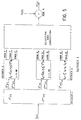
- the concerned 36 bytes are applied to a decoder circuit 1 which computes the syndrome S(x) and transmits it in parallel to those test circuits having a level higher than zero (Decoder 3; Figures 3 and 5).
- the 36 bytes containing one only error are applied to another block, namely Decoder 7, for computation of the new syndrome.
- the test circuit of zero order or level can now operate upon such syndrome, this circuit being capable to correct errors located at a distance equal or less than three.
- the circuit limits itself to outputting an indication that it is not capable to correct the errors occurred.
- a systematic coding technique is adopted in order to maintain the data coefficients (locations 36-5) separate from the control byte coefficients (locations 4-1).
- the error correction code ECC as implemented is byte-oriented due to the specific character of the problem (the memory banks are organized as 16-bit words and the data items are located in memory chips in such a manner as to minimize the effect of the errors upon the data bytes).
- a further problem to be solved is that the shortened or restricted code R-S is not able to detect and correct t errors in the polynomial as received, unless the following condition is fulfilled t ⁇ n/k which, in the present case, is 1.125.
- t ⁇ n/k which, in the present case, is 1.125.
- e d (x) is the polynomial associated with the error relating to the data bytes; its degree is n-k and positions 0, 1, 2, 3 have coefficients equal to zero
- e c (x) is the polynomial associated with error affecting the control bytes; its degree is n-k-1.
- e d (x) can be represented as e d(x) eps .
- This technique is adapted to correct an error in fixed sub-strings of V(x), but it is not adapted to detect and to correct a pair of errors; then a further control is implemented for indicating to the subsequent stage that a second rotation of V(x) may be necessary.
- R r (x) R (r-1) - g (x) (R r-1 n-r , x k-r ) wherein R r (x) is the polynomial at the "r" stage and R r-1 n-r is the (n-r) coefficient of the polynomial.
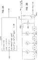
- circuit design aspect it comprises a ladder network to which input signals d(x) and SEL are applied.
- Signal d(x) is coupled to a 8-bit XOR.1 circuit, inserted in a first transverse arm of the ladder, and to a first input of an output multiplexer MUX.
- Signal SEL is coupled to a first gate AND.1 inserted in the first longitudinal leg of the ladder and having its other input connected to said circuit XOR.1.
- circuits a201, a256 and a201 are included, consisting of modulo g(x) 8-bit multiplier circuits.
- the decoder circuit 1 is also implemented as a ladder circuit which receives input signal V(x) and includes in its longitudinal legs the blocks of circuits Decoder 2, Decoder 3 and Decoder 7.
- a first block FIFO.1 is included in its longitudinal parallel leg and comprises an 8-bit FIFO memory which is coupled, together with the output of a first correction block CORR coming from block Decoder 3, to a first node of the ladder incorporating a circuit XOR-5.
- V'(x) The output of this latter circuit, V'(x), is connected to block Decoder 7 and to a second memory block FIFO.2, the output of which is coupled, together with the output of a second correction block CORR', coming from the output of block Decoder 7, to a second node of the ladder also incorporating a circuit XOR.6, and so on.
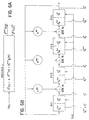
- Figures 4A and 4B respectively show the mathematics and the circuit implementation of block Decoder 2 of Figure 3.
- the circuit comprises four 8-bit multipliers: a92, a182, a189 and a224 which receive in parallel the signal representing V(x) and are connected to four XOR circuits, namely XOR.7, XOR.8, XOR.9. Downstream of each XOR circuit a master-slave flip-flop circuit is inserted; S1(4), S2(4), S3(4), S4(4) the outputs of which are all connected to an output multiplexer circuit MUX.2.
- flip-flop S4 is directly coupled to circuit XOR.7 and is connected to circuits XOR.8, XOR.9 and XOR.10 through 8-bit multipliers a201, a246 and a201, respectively.
- the outputs of all flip-flop circuits are multiplexed by means of a multiplexer circuit MUX.2.
- block Decoder 3 of Figure 3 comprises a first block Decoder 4, to the outputs of which a set of blocks Decoder 5, as well as a Selection and Correction block are connected, the latter block receiving outputs VERR (error value), TANA (indication that an error exists) and CORR (position of the error) from blocks Decoder 5 and outputs VERR and TANA from block Decoder 6.
- the output of the Selection and Correction block is then coupled to a circuit XOR.11 together with a signal V(x) in order to provide an output signal V'(x).
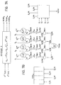
- Block Decoder 4 together with the mathematics implemented therein, is shown in Figures 6A and 6B referring to Figure 6A, it can be seen that block Decoder 4 comprises a set of four double-state, master-slave flip-flop circuits FF.1, FF.2, FF.3, FF.4, interconnected with three XOR circuits XOR.12, XOR.13 and XOR.14.
- the output of the last flip-flop circuit FF.4 is directly coupled to the first flip-flop circuit FF.1 and is connected to above mentioned XOR circuits XOR.12, XOR.13 and XOR.14 by means respective 8-bit multiplier circuits a101, a246 and a201.
- the input signal S(x) is applied in parallel to all four flip-flop circuits.
- Block Decoder 5 the mathematics implemented therein being set forth in Figure 7A, is shown in Figure 7B and will now be described.
- Four input connections S1, S2, S3 and S4 are presented to the circuit for directly reaching four XOR circuits of the already indicated type, namely XOR.15, XOR.16, XOR.17 and XOR.18, as well as four input connections S1 (r+1) , S2 (r+1) , S3 (r+1) , S4 (r+1) for reaching said XOR circuit through respective 8-bit multiplier circuit ⁇ , ⁇ 1, ⁇ 2, ⁇ 3.
- the outputs of said four XOR circuits XOR.15, XOR.16, XOR.17 and XOR.18 are respectively connected to a first input of four NOR gate circuits, namely NOR.1, NOR.2, NOR.3, NOR.4 the outputs of which, in turn, are connected to an input of four AND gate circuits, namely AND.2, AND.3, AND.4 and AND.5 having their outputs ORed to gate circuit OR.1.
- Block Decoder 6 by which the mathematics set forth in Figure 8A is implemented, consists of circuit shown in Figure 8B.
- the circuit comprises three NOR gate circuits, namely NOR.5, NOR.6 and NOR.7 to which signals S1 (r) , S2 (r) and S3 (r) are applied.
- circuit NOR.5 is connected to a first and to a third two-input NAND gate circuits, designated NAND.1 and NAND.3; the output of circuit NOR.6 is connected to said first and a second NAND gate circuits namely NAND.1 and NAND.2; the output of circuit NOR.7 is connected to the inputs of said second and of said third NAND gate circuits, namely NAND.2 and NAND.3.
- the outputs of said circuits NAND.1, NAND.2, and NAND.3 are combined in a further three input NAND gate circuit, NAND.4.
- the output of gate circuit NAND.4 is a signal TANA which, together with signal S4 (r) , is applied to the two inputs of gate circuit AND.6 which provides output signal VERR.
- the output of the fourth flip-flop circuit S4(9) is connected through circuit XOR.23 to circuit XOR.19 and, through three parallel 8-bit multiplier circuits a201, a248, a201 to the other three XOR circuits, XOR.20, XOR.21 and XOR.22.
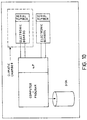
- Such an equipment comprises a computer, for instance of the kind Personal Computer, with enclosed program, associated to a rigid disk unit for storing the specific provisional maps for each device.
- a microprocessor card is designated uP and is adapted
- the electronic boards are housed in said climatic chambers and are standard printed circuits securing the electrical connections between the uP card and twenty memory modules. Such printer circuits are uniquely identified by means of an electronic code stored in the PROM memory.
- the mapping process comprises testing the individual modules mounted upon the electronic board, firstly at high temperature, at 70°C, and then at room temperature, about 25°C, and generating the related error maps.
- the electronic identification of the individual boards enables the high and low temperature maps to be drafted, while maintaining information consistency among the various boards.
- the final map Upon generating the final map, it is permanently stored in the OTP memory included in each individual memory module, under control of the computer and by means of the uP unit.
Landscapes
- Engineering & Computer Science (AREA)
- Theoretical Computer Science (AREA)
- Quality & Reliability (AREA)
- Physics & Mathematics (AREA)
- General Engineering & Computer Science (AREA)
- General Physics & Mathematics (AREA)
- Techniques For Improving Reliability Of Storages (AREA)
- Error Detection And Correction (AREA)
- Hardware Redundancy (AREA)
- Detection And Correction Of Errors (AREA)
Applications Claiming Priority (2)
| Application Number | Priority Date | Filing Date | Title |
|---|---|---|---|
| ITRM930155 | 1993-03-12 | ||
| ITRM930155A IT1261411B (it) | 1993-03-12 | 1993-03-12 | Metodo e circuiteria per l'uso di memorie aventi locazioni difettose erelativa apparecchiatura di produzione. |
Publications (2)
| Publication Number | Publication Date |
|---|---|
| EP0620524A2 true EP0620524A2 (de) | 1994-10-19 |
| EP0620524A3 EP0620524A3 (de) | 1998-08-12 |
Family
ID=11401598
Family Applications (1)
| Application Number | Title | Priority Date | Filing Date |
|---|---|---|---|
| EP94301771A Withdrawn EP0620524A3 (de) | 1993-03-12 | 1994-03-11 | Verbesserungen an Speichern und deren Herstellung |
Country Status (4)
| Country | Link |
|---|---|
| US (1) | US5541938A (de) |
| EP (1) | EP0620524A3 (de) |
| JP (1) | JPH07121451A (de) |
| IT (1) | IT1261411B (de) |
Cited By (1)
| Publication number | Priority date | Publication date | Assignee | Title |
|---|---|---|---|---|
| EP0824237A3 (de) * | 1996-08-05 | 1999-10-06 | Texas Instruments Inc. | Audio-RAM mit Fehlerdetektion und Korrekturfunktion |
Families Citing this family (32)
| Publication number | Priority date | Publication date | Assignee | Title |
|---|---|---|---|---|
| CA2184286C (en) * | 1994-03-04 | 2000-06-06 | Ronald L. Bane | Remote meter reading power reduction method |
| US5909448A (en) * | 1995-09-22 | 1999-06-01 | Advantest Corporation | Memory testing apparatus using a failure cell array |
| US7054271B2 (en) | 1996-12-06 | 2006-05-30 | Ipco, Llc | Wireless network system and method for providing same |
| US8982856B2 (en) | 1996-12-06 | 2015-03-17 | Ipco, Llc | Systems and methods for facilitating wireless network communication, satellite-based wireless network systems, and aircraft-based wireless network systems, and related methods |
| US7079810B2 (en) | 1997-02-14 | 2006-07-18 | Statsignal Ipc, Llc | System and method for communicating with a remote communication unit via the public switched telephone network (PSTN) |
| US6233327B1 (en) | 1997-02-14 | 2001-05-15 | Statsignal Systems, Inc. | Multi-function general purpose transceiver |
| US7137550B1 (en) | 1997-02-14 | 2006-11-21 | Statsignal Ipc, Llc | Transmitter for accessing automated financial transaction machines |
| US5915167A (en) * | 1997-04-04 | 1999-06-22 | Elm Technology Corporation | Three dimensional structure memory |
| US6891838B1 (en) | 1998-06-22 | 2005-05-10 | Statsignal Ipc, Llc | System and method for monitoring and controlling residential devices |
| US6914533B2 (en) | 1998-06-22 | 2005-07-05 | Statsignal Ipc Llc | System and method for accessing residential monitoring devices |
| US6914893B2 (en) | 1998-06-22 | 2005-07-05 | Statsignal Ipc, Llc | System and method for monitoring and controlling remote devices |
| US6437692B1 (en) | 1998-06-22 | 2002-08-20 | Statsignal Systems, Inc. | System and method for monitoring and controlling remote devices |
| US8410931B2 (en) | 1998-06-22 | 2013-04-02 | Sipco, Llc | Mobile inventory unit monitoring systems and methods |
| CN1102271C (zh) * | 1998-10-07 | 2003-02-26 | 国际商业机器公司 | 具有习惯用语处理功能的电子词典 |
| US7103511B2 (en) | 1998-10-14 | 2006-09-05 | Statsignal Ipc, Llc | Wireless communication networks for providing remote monitoring of devices |
| US7263073B2 (en) | 1999-03-18 | 2007-08-28 | Statsignal Ipc, Llc | Systems and methods for enabling a mobile user to notify an automated monitoring system of an emergency situation |
| US7650425B2 (en) | 1999-03-18 | 2010-01-19 | Sipco, Llc | System and method for controlling communication between a host computer and communication devices associated with remote devices in an automated monitoring system |
| AU2001279241A1 (en) | 2000-08-09 | 2002-02-18 | Statsignal Systems, Inc. | Systems and methods for providing remote monitoring of electricity consumption for an electric meter |
| US6725393B1 (en) * | 2000-11-06 | 2004-04-20 | Hewlett-Packard Development Company, L.P. | System, machine, and method for maintenance of mirrored datasets through surrogate writes during storage-area network transients |
| ITRM20010298A1 (it) * | 2001-05-31 | 2002-12-02 | Micron Technology Inc | Interfaccia di comando di utilizzatore con decodificatore programmabile. |
| US6678836B2 (en) * | 2001-01-19 | 2004-01-13 | Honeywell International, Inc. | Simple fault tolerance for memory |
| US7346463B2 (en) | 2001-08-09 | 2008-03-18 | Hunt Technologies, Llc | System for controlling electrically-powered devices in an electrical network |
| US7480501B2 (en) | 2001-10-24 | 2009-01-20 | Statsignal Ipc, Llc | System and method for transmitting an emergency message over an integrated wireless network |
| US8489063B2 (en) | 2001-10-24 | 2013-07-16 | Sipco, Llc | Systems and methods for providing emergency messages to a mobile device |
| US7424527B2 (en) | 2001-10-30 | 2008-09-09 | Sipco, Llc | System and method for transmitting pollution information over an integrated wireless network |
| US7325157B2 (en) * | 2003-11-03 | 2008-01-29 | Samsung Electronics Co., Ltd | Magnetic memory devices having selective error encoding capability based on fault probabilities |
| US8031650B2 (en) | 2004-03-03 | 2011-10-04 | Sipco, Llc | System and method for monitoring remote devices with a dual-mode wireless communication protocol |
| US7756086B2 (en) | 2004-03-03 | 2010-07-13 | Sipco, Llc | Method for communicating in dual-modes |
| US9439126B2 (en) | 2005-01-25 | 2016-09-06 | Sipco, Llc | Wireless network protocol system and methods |
| CN103390588B (zh) * | 2012-05-09 | 2015-08-19 | 无锡华润上华半导体有限公司 | 一种基于otp存储器制作mrom存储器的方法 |
| US10903858B2 (en) * | 2015-05-27 | 2021-01-26 | Quantum Corporation | Dynamically variable error correcting code (ECC) system with hybrid rateless reed-solomon ECCs |
| US11119909B2 (en) * | 2018-12-11 | 2021-09-14 | Texas Instmments Incorporated | Method and system for in-line ECC protection |
Family Cites Families (6)
| Publication number | Priority date | Publication date | Assignee | Title |
|---|---|---|---|---|
| US4653050A (en) * | 1984-12-03 | 1987-03-24 | Trw Inc. | Fault-tolerant memory system |
| IT1201837B (it) * | 1986-07-22 | 1989-02-02 | Sgs Microelettronica Spa | Sistema per la verifica della funzionalita' e delle caratteristiche di dispositivi a semiconduttore di tipo eprom durante il "burn-in" |
| US4939694A (en) * | 1986-11-03 | 1990-07-03 | Hewlett-Packard Company | Defect tolerant self-testing self-repairing memory system |
| US5067105A (en) * | 1987-11-16 | 1991-11-19 | International Business Machines Corporation | System and method for automatically configuring translation of logical addresses to a physical memory address in a computer memory system |
| US5077737A (en) * | 1989-08-18 | 1991-12-31 | Micron Technology, Inc. | Method and apparatus for storing digital data in off-specification dynamic random access memory devices |
| EP0584864B1 (de) * | 1992-08-21 | 1997-11-05 | Koninklijke Philips Electronics N.V. | Hardware-effizientes Verfahren und Anordnung zur Kodierung von BCH-Kodes und insbesondere Reed-Solomon-Kodes |
-
1993
- 1993-03-12 IT ITRM930155A patent/IT1261411B/it active IP Right Grant
-
1994
- 1994-03-11 US US08/209,580 patent/US5541938A/en not_active Expired - Lifetime
- 1994-03-11 EP EP94301771A patent/EP0620524A3/de not_active Withdrawn
- 1994-03-14 JP JP6080844A patent/JPH07121451A/ja active Pending
Cited By (1)
| Publication number | Priority date | Publication date | Assignee | Title |
|---|---|---|---|---|
| EP0824237A3 (de) * | 1996-08-05 | 1999-10-06 | Texas Instruments Inc. | Audio-RAM mit Fehlerdetektion und Korrekturfunktion |
Also Published As
| Publication number | Publication date |
|---|---|
| IT1261411B (it) | 1996-05-23 |
| US5541938A (en) | 1996-07-30 |
| ITRM930155A0 (it) | 1993-03-12 |
| ITRM930155A1 (it) | 1994-09-12 |
| EP0620524A3 (de) | 1998-08-12 |
| JPH07121451A (ja) | 1995-05-12 |
Similar Documents
| Publication | Publication Date | Title |
|---|---|---|
| US5541938A (en) | Method and apparatus for mapping memory as to operable and faulty locations | |
| US5784391A (en) | Distributed memory system with ECC and method of operation | |
| US7370264B2 (en) | H-matrix for error correcting circuitry | |
| US5099484A (en) | Multiple bit error detection and correction system employing a modified Reed-Solomon code incorporating address parity and catastrophic failure detection | |
| US5418796A (en) | Synergistic multiple bit error correction for memory of array chips | |
| US8291303B2 (en) | Memory device with error correction system for detection and correction errors in read out data | |
| EP0668561B1 (de) | Flexible Fehlerkorrekturcode/Paritätsbit-Architektur | |
| US4413339A (en) | Multiple error detecting and correcting system employing Reed-Solomon codes | |
| US5226043A (en) | Apparatus and method for data error detection and correction and address error detection in a memory system | |
| US4277844A (en) | Method of detecting and correcting errors in digital data storage systems | |
| EP0497110B1 (de) | Verfahren und Einrichtung zur Fehlererkennung in Recherspeichern versehen mit Mehrfach-bit-Ausgängen | |
| US6076182A (en) | Memory fault correction system and method | |
| US4961193A (en) | Extended errors correcting device having single package error correcting and double package error detecting codes | |
| US20040225944A1 (en) | Systems and methods for processing an error correction code word for storage in memory components | |
| JPS59197940A (ja) | 誤り検出・補正メモリ | |
| US7873895B2 (en) | Memory subsystems with fault isolation | |
| US4631725A (en) | Error correcting and detecting system | |
| KR970707493A (ko) | 디스크 드라이브 에뮬레이터를 위한 에러 보정 방법및 장치(error correction method and apparatus for disk drive emulator) | |
| JPS6116351A (ja) | システムメモリ用単一誤り訂正回路 | |
| US20100011247A1 (en) | Method and apparatus for parallel ecc error location | |
| US5450423A (en) | Data error correcting/detecting system and apparatus compatible with different data bit memory packages | |
| JPS62117200A (ja) | 自己テスト機能付き半導体メモリおよび自己テスト方法 | |
| US5691996A (en) | Memory implemented error detection and correction code with address parity bits | |
| US20020157059A1 (en) | Multipurpose method for constructing an error-control code for multilevel memory cells operating with a variable number of storage levels, and multipurpose error-control method using said error-control code | |
| US20190310910A1 (en) | Memory system and operating method of the memory system |
Legal Events
| Date | Code | Title | Description |
|---|---|---|---|
| PUAI | Public reference made under article 153(3) epc to a published international application that has entered the european phase |
Free format text: ORIGINAL CODE: 0009012 |
|
| AK | Designated contracting states |
Kind code of ref document: A2 Designated state(s): DE FR GB IT NL |
|
| PUAL | Search report despatched |
Free format text: ORIGINAL CODE: 0009013 |
|
| AK | Designated contracting states |
Kind code of ref document: A3 Designated state(s): DE FR GB IT NL |
|
| STAA | Information on the status of an ep patent application or granted ep patent |
Free format text: STATUS: THE APPLICATION IS DEEMED TO BE WITHDRAWN |
|
| 18D | Application deemed to be withdrawn |
Effective date: 19990213 |