EP0617796B1 - Digitales strahlformungsarray - Google Patents
Digitales strahlformungsarray Download PDFInfo
- Publication number
- EP0617796B1 EP0617796B1 EP92924837A EP92924837A EP0617796B1 EP 0617796 B1 EP0617796 B1 EP 0617796B1 EP 92924837 A EP92924837 A EP 92924837A EP 92924837 A EP92924837 A EP 92924837A EP 0617796 B1 EP0617796 B1 EP 0617796B1
- Authority
- EP
- European Patent Office
- Prior art keywords
- digital
- signal
- signals
- weighting
- beamforming
- Prior art date
- Legal status (The legal status is an assumption and is not a legal conclusion. Google has not performed a legal analysis and makes no representation as to the accuracy of the status listed.)
- Expired - Lifetime
Links
- 238000000034 method Methods 0.000 claims description 32
- 230000003111 delayed effect Effects 0.000 claims description 10
- 238000010079 rubber tapping Methods 0.000 claims description 10
- 238000007792 addition Methods 0.000 claims description 7
- 238000007493 shaping process Methods 0.000 claims description 5
- 230000015572 biosynthetic process Effects 0.000 claims description 2
- 230000001419 dependent effect Effects 0.000 claims 3
- 230000008901 benefit Effects 0.000 abstract description 8
- 238000005516 engineering process Methods 0.000 abstract description 4
- 238000005070 sampling Methods 0.000 description 18
- 230000008569 process Effects 0.000 description 13
- 238000006243 chemical reaction Methods 0.000 description 4
- 230000001934 delay Effects 0.000 description 4
- 230000009467 reduction Effects 0.000 description 4
- 230000003044 adaptive effect Effects 0.000 description 2
- 238000012545 processing Methods 0.000 description 2
- 238000012935 Averaging Methods 0.000 description 1
- 238000003491 array Methods 0.000 description 1
- 238000007796 conventional method Methods 0.000 description 1
- 238000011161 development Methods 0.000 description 1
- 230000018109 developmental process Effects 0.000 description 1
- 238000003384 imaging method Methods 0.000 description 1
- 238000010348 incorporation Methods 0.000 description 1
- 238000012986 modification Methods 0.000 description 1
- 230000004048 modification Effects 0.000 description 1
- 230000003287 optical effect Effects 0.000 description 1
- 238000002604 ultrasonography Methods 0.000 description 1
Images


Classifications
-
- H—ELECTRICITY
- H01—ELECTRIC ELEMENTS
- H01Q—ANTENNAS, i.e. RADIO AERIALS
- H01Q3/00—Arrangements for changing or varying the orientation or the shape of the directional pattern of the waves radiated from an antenna or antenna system
- H01Q3/26—Arrangements for changing or varying the orientation or the shape of the directional pattern of the waves radiated from an antenna or antenna system varying the relative phase or relative amplitude of energisation between two or more active radiating elements; varying the distribution of energy across a radiating aperture
-
- G—PHYSICS
- G01—MEASURING; TESTING
- G01S—RADIO DIRECTION-FINDING; RADIO NAVIGATION; DETERMINING DISTANCE OR VELOCITY BY USE OF RADIO WAVES; LOCATING OR PRESENCE-DETECTING BY USE OF THE REFLECTION OR RERADIATION OF RADIO WAVES; ANALOGOUS ARRANGEMENTS USING OTHER WAVES
- G01S13/00—Systems using the reflection or reradiation of radio waves, e.g. radar systems; Analogous systems using reflection or reradiation of waves whose nature or wavelength is irrelevant or unspecified
- G01S13/02—Systems using reflection of radio waves, e.g. primary radar systems; Analogous systems
- G01S13/06—Systems determining position data of a target
- G01S13/46—Indirect determination of position data
- G01S13/48—Indirect determination of position data using multiple beams at emission or reception
-
- G—PHYSICS
- G01—MEASURING; TESTING
- G01S—RADIO DIRECTION-FINDING; RADIO NAVIGATION; DETERMINING DISTANCE OR VELOCITY BY USE OF RADIO WAVES; LOCATING OR PRESENCE-DETECTING BY USE OF THE REFLECTION OR RERADIATION OF RADIO WAVES; ANALOGOUS ARRANGEMENTS USING OTHER WAVES
- G01S13/00—Systems using the reflection or reradiation of radio waves, e.g. radar systems; Analogous systems using reflection or reradiation of waves whose nature or wavelength is irrelevant or unspecified
- G01S13/87—Combinations of radar systems, e.g. primary radar and secondary radar
Definitions
- This invention relates to a digital beamforming array for use in radar applications and in particular in radar applications that use phased array technology.
- Such sensors comprise an array of modules, each having its own independent transmitter and receiver.
- Electronically steered transmit and receive beams can be generated by suitable phasing of the input and output signals of the modules. This enables rapid beam steering without moving mechanical parts, giving enhanced potential for multi-mode operation and/or low cost implementation.
- Numerous developments of this technique have been described in the prior art.
- US 4 688 045 describes such phased array beamsteering, the phasing being achieved by selectively delaying the output of each module. The delays required are determined by a novel algorithm which relates these delays to the desired steering direction.
- EP 0 224 014 is concerned with medical ultrasound imaging in which a high level of focusing accuracy is required. This document discloses the use of non-uniform sampling rates across array components in order to overcome the limitation of time delay resolution to the sampling period, and corresponding bandwidth limitation to one half the sampling rate of the analogue to digital convener.
- One particular analogue to digital converter usable in both radar and ultrasonic applications is the delta sigma converter.
- Such converters are described in more detail hereinbelow and in JP 3 114 449. Briefly, they comprise a high-speed one-bit analogue to digital converter (a delta sigma tracker) and a decimating filter which converts this one-bit data to a multi-bit output.
- JP 3 114 449 discloses how a reduction in complexity of phased array ultrasonic devices can be achieved by implementing the time delays at the one-bit stage. The delayed one-bit data streams are summed in an adder and the decimating filer is then applied to the adder output. Conventionally the time delays had been applied to the multi-bit delta sigma converter outputs.
- the device described in JP 3 114 449 achieves an overall reduction in device complexity.
- smaller groups of one-bit data streams are time delayed and fed into respective adders and cascaded time delay and adder stages are used to generate the final summed output. This output is again input to a single decimating filter.
- Digital beamforming enables multiple receive beams to be implemented without the need for many bulky analogue beamforming manifolds. This ability to realise multiple receive beams is vital if monopulse or other precision target bearing determination schemes are to be implemented. Also the ability to sample the output of each module independently allows the implementation of adaptive beamforming and super-resolution algorithms, which are currently reaching a high degree of maturity.
- the algorithmic nature of the beamforming process means that it is possible for variations in the phase and amplitude responses of individual modules to be calibrated out by software means.
- the present invention provides a digital beamforming array combining a reduction in complexity and cost with all the advantages of digital beamforming mentioned above.
- a digital beamforming array including:
- the weighting means may be arranged to provide for non-uniform amplitude weighting to counteract variation in sensor module characteristics and / or to improve array sidelobe characteristics.
- the beamforming process according to the present invention involves the combination of suitably phase shifted n-bit representations of the sensor module outputs. This would appear to involve high-speed complex digital multiplications.
- the beamforming process can be implemented by a beamforming means which includes respective time delay means for each digitising means arranged to delay the digital signals relative to one another and the beamforming means includes at least one adding means ranged to add together signals of a set of delayed signals.
- each digitising means can be regarded as a representation of the output of the relevant sensor module. If the digitising means oversamples by a factor Q, then each n-bit output forms a series of discrete signals which represent the output of the relevant sensor module at intervals in phase of 2 ⁇ /Q.
- the beamforming process aims primarily to remove phase differences between received signals which result from the angle of incidence of a received beam on the spatially separated ray of sensor modules. This process is generally carried out by altering the phase angles of the received signals relative to one another in a predetermined manner depending on the said angle of incidence.
- beamforming can be achieved simply by time delaying the n-bit outputs relative to one another, which is equivalent to delaying the outputs by multiples of 2 ⁇ /Q in phase angle relative to one another and then adding the n-bit outputs so delayed. Therefore, this preferred embodiment of the present invention significantly reduces the cost and complexity of the signal processing hardware required to implement the beamforming process.
- the beamforming means includes a plurality of adding means each arranged to add together signals of a respective set of delayed signals as appropriate to form multiple beams.
- Incident beams may arrive at the ray from a spread of directions and so it may be necessary in some applications to implement the beams in a number of different directions within this spread.
- the present invention is easily adapted for this purpose because different sets of signals, delayed in accordance with different angles of incidence, can be fed to each adding means.
- each time delay means comprises a shift register having a number of elements each for storing an n-bit signal and the beamforming means includes means for tapping register elements to obtain time delayed signals for addition in the adding means.
- the n-bit signals held in successive elements of the shift register are representations of the signal from the sensor module shifted in phase by 2 ⁇ /Q.
- tapping a signal from the appropriate element of each shift register a set of signals with the appropriate relative phase changes made to them (in multiples of 2 ⁇ /Q) can be obtained.
- the use of the shift registers as time delay means enables a further reduction in the cost and complexity of the beamforming array according to the present invention.
- the digitising means preferably includes signal comparing means incorporating an analogue reference voltage wherein the weighting means is arranged to implement non-uniform amplitude weighting by variation of the analogue reference voltage.
- the weighting means may be arranged to implement non-uniform amplitude weighting by multiplication of the digital signals by a weighting sequence. Such multiplication of the digital signals may be achieved prior to or after tapping the shift register elements.
- the oversampling factor of the digitising means, Q is greater than 16 so that the relative differences in phase that can be introduced into the n-bit signals are small enough to allow accurate beamforming. More preferably the oversampling factor, Q, is greater than 32.
- the intermediate frequency signal In applications where the information flow rate allows, it is preferable to convert the intermediate frequency signal to a one-bit digital signal at the oversampling rate.
- the rate of oversampling is greatest for a one-bit signal and so where the information flow is high the oversampling rate may exceed the capabilities of the digitising hardware and so conversion to a one-bit signal is not possible.
- the advantage of a conversion to a one-bit digital signal is that it can be manipulated by simple hardware which can be cheap and reliable. For example one-bit shift registers and one-bit adders.
- the raw digital information would require a multi-pin connector to interface the data to the beamforming processor.
- connection is expensive and can be unreliable in applications where high vibrations are likely to be experienced.
- Such a connection can be avoided in this preferred embodiment of the present invention because the interface is made at one-bit level which does not require complex hardware. Also, if a wire-less connection is required a simple one-bit optical data link can be used.
- each digitising means comprises the first part and the decimating means comprises the second part of a delta sigma analogue to digital converter.
- the decimating filter of a delta sigma converter performs an energy averaging process over portions of the one-bit stream from the first part of the converter. This process is linear, as is the process of beamforming, so the beamforming process can be performed on the one-bit data from the first part of the converter, which beamformed data can then be averaged in the decimating filter.
- the advantages of using delta sigma converters are not lost by splitting the two parts of the converter as in the present invention and JP 3 114 449.
- delta sigma converters have a high dynamic range which is important in applications which require the operation of the beamforming array in high clutter and electronic interference environments. They also have the advantage of allowing low cost monolithic implementation.
- the linear digitising means could utilise analogue to digital conversion using direct interpolation as described in US Patent No. 4, 621, 254, entitled “Apparatus and Method for Analogue to Digital Conversion".
- the trade off between the number of bits and the rate of oversampling makes it is preferable to use a number of bits that is greater than 1.
- the digitising means to comprise the first part and the decimating means to comprise the second part of a noise shaping analogue to digital converter.
- a method for digitally beamforming a signal comprising the steps of:
- the weighting step may be arranged to counteract variation in sensor characteristics and / or to improve array sidelobe characteristics.
- the beamforming method includes performing a plurality of additions in each of which signals of a respective set of digital signals are added together as appropriate to form multiple beams.
- the beamforming method preferably comprises the steps of time delaying the digital signals in shift registers each having a number of elements, each element being capable of storing an n-bit digital signal and register elements being tapped to obtain time-delayed signals for addition.
- the weighting step may be implemented either by varying an analogue reference voltage applied to a signal comparing means within the digitising means or by multiplying the digital signals with a weighting sequence.
- the weighting step may implemented prior to tapping the shift register elements and it may be implemented by multiplying each signal stored in respective shift registers with a weighting sequence and overwriting each signal by the respective multiplied signal.
- tapping the shift register elements may be carried out prior to implementing the weighting step.
- the method according to the second aspect of the present invention has the same advantages as are discussed above in relation to the first aspect of the present invention
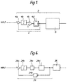
- the delta sigma converter 2 shown therein can be divided into two parts.
- the first part is an analogue one-bit sampling loop 4 and is a high speed one-bit analogue to digital convener which samples at a speed many times higher than the sampling rate necessary for the required signal bandwidth.
- the one-bit sampling loop 4 comprises a subtracting means 4a, an integrator 4b, a comparator 4c (which compares an input signal with an analogue voltage reference level) and a latch circuit 4d, connected in series in a loop. This produces an output from the latch circuit 4d which is a rapid stream of one-bit data at the oversampling rate.
- the decimating filter 6 In order to produce multi-bit data at the required signal bandwidth, it is necessary to feed this data into the second part of the delta sigma convener, the decimating filter 6.
- the decimating filter 6 normally comprises a cascade of filters operating at successively lower sampling rates, culminating in the desired multi-bit output.
- this shows a conventional digitally beamformed array comprising an array of j antennae 8 1 to 8 j which are arranged in a straight line.
- the outputs from each antenna 8 1 to 8 j are fed into respective transmit/receive modules 10 1 to 10 j which each have their own transmitting and receiving circuitry.
- the intermediate frequency outputs of the transmit/receive modules 10 1 to 10 j are fed into respective delta sigma converters 2 1 to 2 j , which operate as discussed above with reference to Figure 1.
- the outputs from all the delta sigma converters 2 1 to 2 j are connected to a single digital beamformer 12.
- the digitally beamformed array shown in Figure 2 operates in the following way.
- the signals received by the antennae 8 1 to 8 j are convened to intermediate frequency in the respective transmit receive modules 10 1 to 10 j .
- the intermediate frequency signals are then digitised by the sigma-delta converters 2 1 to 2 j .
- these digital representations of each of the n received signals are beamformed in the digital beamformer 12, to remove the differences in the phase between the signals, associated with a radar pulse incident at the said angle q.
- the signal output from the digital beamformer 12 can then be analysed to obtain information about any target that is located in the direction associated with the angle q.
- the array shown in Figure 2 is complex and relatively expensive because one delta sigma converter is required for each module and the digital beamformer 12 is a complex signal processor which has to be able to carry out high speed complex multiplications on the multi-bit information from the converters.
- FIG. 3 shows a digitally beamformed array according to the present invention comprising an array of j antennae 8 1 to 8j which are arranged in a straight line, similarly to the array shown in Figure 2. Also similar to the array shown in Figure 2 are the transmit/receive modules 10 1 to 10 j .
- the intermediate frequency outputs of the transmit receive modules 10 1 to 10 j are fed into the analogue one bit sampling loops 4 1 to 4 j respectively which form the first half of a delta sigma converter 2, as discussed with reference to Figure 1.
- the process of beamforming can be accomplished by simply adding together suitably time-delayed oversampled outputs of the sampling loops 4 1 to 4 j .
- the outputs of the sampling loops are fed into shift registers 14 1 to 14 j respectively, each of which is Q elements (each element is able to store a one-bit number) long and the outputs 18 1 to 18 j of appropriate shift register elements are summed in a one-bit beam adder 16.
- the output of the beam adder 16 is then fed into a decimating filter 6.
- the output of the decimating filter 6 will be similar to the output of the beamformer 12 of Figure 2 and can be analysed in a similar way to obtain target information.
- Multiple beams for example in monopulse applications, can be simply implemented by incorporating further adders, for example 22 in Figure 3, fed from outputs 20 1 to 20 j of other elements of the shift registers 14 1 to 14 j as shown in Figure 3 in dotted lines.
- the digitally beamformed array described above in relation to Figure 3 implements a uniform weighting across the elements that are added in the beam adders 16 (and 22), there being no provision for individually changing the weight given to the individual elements in the addition.
- the outputs of the sensor modules are required to be non-uniformly weighted, in order to improve the sidelobes of the resulting pattern.
- This can be achieved by either varying the analogue voltage reference levels of the individual converters 4 1 to 4 j or alternatively by multiplying the l-bit oversampled outputs of the converters 4 1 to 4 j by a suitable l-bit weighting sequence prior to being fed to the adders 16 (and 22).
- This latter operation can be either applied before or after the shift registers 14 1 to 14 j depending on whether the same or different weightings are required for the group of signals fed into the different adders 16 and 22.
- a type of analogue to digital converter with this property is a noise shaping analogue to digital converter, such as is shown in Figure 4.
- Such a converter can also be split into a sampling loop 24 and a decimating filter 26 in a similar manner to the delta sigma converter of Figure 1.
- the sampling loop 24 comprises a subtraction means 24a, an integrator 24b, an n-bit analogue to digital converter 24c, a latch circuit 24d and a digital to analogue converter 24e, connected in series in a loop.
- the output of the latch circuit 24d is a series of n-bit representations of the signal from the sensor module at an oversampled rate. If the first part of a noise shaping analogue to digital convener, the sampling loop 24, is used to produce an output of n-bit data in place of each one of the sampling loops 4 1 to 4 j in the array shown in Figure 3 then n-bit element shift registers can be used instead of the l-bit element shift registers 14 1 to 14 j and an n-bit adder can be used in place of the one-bit adder 16.
- a suitable decimating filter 6 could then be used to convert the resulting data to the number of bits required to represent the entire dynamic range of the intermediate frequency signal.
Landscapes
- Engineering & Computer Science (AREA)
- Radar, Positioning & Navigation (AREA)
- Remote Sensing (AREA)
- Computer Networks & Wireless Communication (AREA)
- Physics & Mathematics (AREA)
- General Physics & Mathematics (AREA)
- Radar Systems Or Details Thereof (AREA)
- Optical Communication System (AREA)
- Holo Graphy (AREA)
- Apparatus For Radiation Diagnosis (AREA)
- Internal Circuitry In Semiconductor Integrated Circuit Devices (AREA)
- Variable-Direction Aerials And Aerial Arrays (AREA)
Claims (25)
- Digitales Strahlformungsarray mit:dadurch gekennzeichnet, daß(a) mehreren Sensormodulen (8, 10) zum Erzeugen von Zwischenfrequenzsignalen (IF) aus empfangenen Signalen,(b) einer Digitalisierungsvorrichtung (4) zum Umwandeln des IF-Signals in digitale n-Bit-Signale mit einer Oversampling-Rate, wobei n kleiner als die Zahl der Bits ist, die erforderlich sind, um den IF-Signal-Dynamikbereich darzustellen,(c) einer Strahlformungsvorrichtung (14, 16) zum Verändern der Phasen der digitalen Signale in bezug aufeinander und zu ihrem Überlagern, um ein resultierendes Signal zu bilden, und(d) einer Decimating-Vorrichtung (6) zum Umwandeln des resultierenden Signals in ein Mehr-Bit-Signal mit einer Anzahl von-Bits, die wenigstens gleich der ist, die erforderlich ist, um den IF-Signal-Dynamikbereich darzustellen,
das Array außerdem eine Wichtungsvorrichtung (4c, 14, 16) umfaßt, um dafür zu sorgen, daß die digitalen Signale eine ungleichförmige Wichtung vor der Bildung des resultierenden Signals erfahren. - Digitales Strahlformungsarray nach Anspruch 1, dadurch gekennzeichnet, daß die Wichtungsvorrichtung (4c, 14, 16) dazu dient, eine ungleichförmige Amplitudenwichtung zu bewirken, um Schwankungen bei den Sensormoduleigenschaften entgegenzuwirken.
- Digitales Strahlformungsarray nach Anspruch 1 oder 2, dadurch gekennzeichnet, daß die Wichtungsvorrichtung (4c, 14, 16) dazu dient, die Seitenkeuleneigenschaften zu verbessern.
- Digitales Strahlformungsarray nach Anspruch 1, 2 oder 3, dadurch gekennzeichnet, daß die Strahlformungsvorrichtung (14, 16) eine jeweilige Zeitverzögerungsvorrichtung (14) für jede Digitalisierungsvorrichtung (4) umfaßt, um die digitalen Signale in bezug aufeinander zu verzögern, und die Strahlformungsvorrichtung (14, 16) wenigstens eine Addierervorrichtung (16) umfaßt, um die Signale einer Menge von verzögerten Signalen zusammenzuzählen.
- Digitales Strahlformungsarray nach Anspruch 4, dadurch gekennzeichnet, daß die Strahlformungsvorrichtung (14, 16) mehrere Addierervorrichtungen (16) umfaßt, die jeweils dazu dienen, Signale einer jeweiligen Menge von verzögerten Signalen geeignet zu addieren, um Mehrfachstrahlen zu erzeugen.
- Digitales Strahlformungsarray nach Anspruch 4 oder 5, dadurch gekennzeichnet, daß jede Zeitverzögerungsvorrichtung ein Schieberegister (14) mit einer Anzahl von Elementen umfaßt, die jeweils zum Speichern eines digitalen n-Bit-Signals dienen, und die Strahlformungsvorrichtung (14, 16) eine Vorrichtung zum Auslesen von Registerelementen umfaßt, um zeitverzögerte Signale für die Addition in der Addierervorrichtung (16) zu erhalten.
- Digitales Strahlformungsarray nach einem der vorangehenden Ansprüche, dadurch gekennzeichnet, daß die Digitalisierungsvorrichtung (4) eine Signalvergleichsvorrichtung umfaßt, die eine analoge Referenzspannung umfaßt, wobei die Wichtungsvorrichtung (4c) dazu dient, eine ungleichförmige Amplitudenwichtung durch Variation der analogen Referenzspannung zu implementieren.
- Digitales Strahlformungsarray nach einem der Ansprüche 1 bis 6, dadurch gekennzeichnet, daß die Wichtungsvorrichtung (14, 16) dazu dient, eine ungleichförmige Amplitudenwichtung durch Multiplikation der digitalen Signale mit einer Wichtungssequenz zu implementieren.
- Digitales Strahlformungsarray nach Anspruch 8, soweit dieser sich auf Anspruch 6 bezieht, dadurch gekennzeichnet, daß die Wichtungsvorrichtung ausgelegt ist für die Multiplikation des digitalen Signals vor dem Auslesen der Schieberegisterelemente.
- Digitales Strahlformungsarray nach Anspruch 8, dadurch gekennzeichnet, daß die Wichtungsvorrichtung ausgelegt ist für die Multiplikation der digitalen Signale nach Auslesen der Schieberegisterelemente.
- Digitales Strahlformungsarray nach einem der vorangehenden Ansprüche, dadurch gekennzeichnet, daß der Faktor des Oversampling Q größer als 16 ist.
- Digitales Strahlformungsarray nach einem der vorangehenden Ansprüche, dadurch gekennzeichnet, daß n gleich 1 ist.
- Digitales Strahlformungsarray nach Anspruch 12, dadurch gekennzeichnet, daß jede Digitalisierungsvorrichtung (4) den ersten Teil und die Decimating-Vorrichtung (6) den zweiten Teil eines Delta/Sigma-Analog/Digital-Konverters umfaßt.
- Digitales Strahlformungsarray nach einem der Ansprüche 1 bis 11, dadurch gekennzeichnet, daß n größer als 1 ist.
- Digitales Strahlformungsarray nach Anspruch 14, dadurch gekennzeichnet, daß jede Digitalisierungsvorrichtung (24) den ersten Teil und die Decimating-Vorrichtung (26) den zweiten Teil eines rauschfilternden Analog/Digital-Konverters umfaßt.
- Verfahren für das digitale Strahlformen eines Signals mit den Schritten:dadurch gekennzeichnet, daß(a) Empfangen des bei mehreren Sensoren eines phasengesteuerten Arrays ankommenden Signals und Erzeugen eines jeweiligen IF-Signals davon bei jedem Modul,(b) Wandeln des IF-Signals in digitale n-Bit-Signale mit einer Oversampling-Rate, wobei n kleiner als die Zahl der Bits ist, die erforderlich ist, um den Dynamikbereich des IF-Signals darzustellen,(c) Strahlformen der digitalen n-Bit-Signale durch Ändern ihrer relativen Phasen und Überlagern von ihnen, um ein resultierendes Signal zu erzeugen, und(d) Wandeln des resultierenden Signals in ein Mehr-Bit-Signal mit der Anzahl von-Bits, die erforderlich ist, um den Dynamikbereich des IF-Signals darzustellen,
das Verfahren als zusätzlichen Schritt das Anwenden einer ungleichförmigen Amplitudenwichtung auf die digitalen Signale vor Bilden des resultierenden Signals umfaßt. - Verfahren nach Anspruch 16, dadurch gekennzeichnet, daß der Wichtungsschritt ausgelegt ist, Schwankungen der Sensoreigenschaften entgegenzuwirken.
- Verfahren nach Anspruch 15 oder 16, dadurch gekennzeichnet, daß der Wichtungsschritt ausgelegt ist, die Seitenkolbeneigenschaften des Arrays zu verbessern.
- Verfahren nach Anspruch 16, 17 oder 18, dadurch gekennzeichnet, daß das Strahlformen das Ausführen mehrerer Additionen umfaßt, wobei bei jeder Signale einer jeweiligen Menge von digitalen Signalen je nach Eignung zusammengezählt werden, um Mehrfachstrahlen zu bilden.
- Verfahren nach Anspruch 19, dadurch gekennzeichnet, daß das Strahlformen ein Zeitverzögern der digitalen Signale in Schieberegistern (14) umfaßt, wobei jedes eine Anzahl von Elementen umfaßt, wobei jedes Element dazu geeignet ist, digitale n-Bit-Signale abzuspeichern, und wobei Registerelemente ausgelesen werden, um zeitverzögerte Signale für die Addition zu erhalten.
- Verfahren nach einem der Ansprüche 16 bis 20, dadurch gekennzeichnet, daß der Wichtungsschritt implementiert wird, indem eine analoge Referenzspannung, die an der Signalvergleichsvorrichtung (4c) innerhalb der Digitalisierungsvorrichtung (4) anliegt, variiert wird.
- Verfahren nach einem der Ansprüche 16 bis 20, dadurch gekennzeichnet, daß der Wichtungsschritt implementiert wird durch Multiplizieren der digitalen Signale mit einer Wichtungssequenz.
- Verfahren nach Anspruch 22, soweit dieser sich auf Anspruch 20 bezieht, dadurch gekennzeichnet, daß der Wichtungsschritt implementiert wird vor dem Auslesen der Schieberegisterelemente.
- Verfahren nach Anspruch 23, dadurch gekennzeichnet, daß der Wichtungsschritt implementiert wird durch Multiplizieren jedes Signals, das in den jeweiligen Schieberegistern abgespeichert ist, mit einer Wichtungssequenz und Überschreiben jedes Signals durch das jeweilige multiplizierte Signal.
- Verfahren nach Anspruch 22, soweit er sich auf Anspruch 20 bezieht, dadurch gekennzeichnet, daß das Auslesen der Schieberegisterelemente ausgeführt wird vor dem Implementieren des Wichtungsschrittes.
Applications Claiming Priority (3)
| Application Number | Priority Date | Filing Date | Title |
|---|---|---|---|
| GB919126944A GB9126944D0 (en) | 1991-12-19 | 1991-12-19 | A digital beamforming array |
| GB9126944 | 1991-12-19 | ||
| PCT/GB1992/002317 WO1993012440A1 (en) | 1991-12-19 | 1992-12-14 | A digital beamforming array |
Publications (2)
| Publication Number | Publication Date |
|---|---|
| EP0617796A1 EP0617796A1 (de) | 1994-10-05 |
| EP0617796B1 true EP0617796B1 (de) | 2000-02-16 |
Family
ID=10706517
Family Applications (1)
| Application Number | Title | Priority Date | Filing Date |
|---|---|---|---|
| EP92924837A Expired - Lifetime EP0617796B1 (de) | 1991-12-19 | 1992-12-14 | Digitales strahlformungsarray |
Country Status (9)
| Country | Link |
|---|---|
| US (1) | US5461389A (de) |
| EP (1) | EP0617796B1 (de) |
| JP (1) | JP3258010B2 (de) |
| AT (1) | ATE189841T1 (de) |
| DE (1) | DE69230692T2 (de) |
| DK (1) | DK0617796T3 (de) |
| ES (1) | ES2141730T3 (de) |
| GB (2) | GB9126944D0 (de) |
| WO (1) | WO1993012440A1 (de) |
Cited By (2)
| Publication number | Priority date | Publication date | Assignee | Title |
|---|---|---|---|---|
| US8982931B2 (en) | 2013-03-15 | 2015-03-17 | Raytheon Company | RF puck |
| US10698083B2 (en) | 2017-08-25 | 2020-06-30 | Raytheon Company | Method and apparatus of digital beamforming for a radar system |
Families Citing this family (31)
| Publication number | Priority date | Publication date | Assignee | Title |
|---|---|---|---|---|
| WO1994005782A1 (en) * | 1992-09-10 | 1994-03-17 | Trustees Of Tufts College | In vivo production of transgenic organ by introducing the transgene via lumen |
| US6081566A (en) * | 1994-08-02 | 2000-06-27 | Ericsson, Inc. | Method and apparatus for interference rejection with different beams, polarizations, and phase references |
| EP0700116A3 (de) * | 1994-08-29 | 1998-01-07 | Atr Optical And Radio Communications Research Laboratories | Vorrichtung und Verfahren zur Steuerung einer Gruppenantenne mit einer Vielzahl von Antennenelementen für verbesserte einkommende Strahlverfolgung |
| US5552791A (en) * | 1995-04-07 | 1996-09-03 | Northrop Grumman Corporation | Fiber optic telemetry array calibration system |
| US5610613A (en) * | 1995-09-15 | 1997-03-11 | Raytheon Company | Analog to digital conversion system |
| US5909460A (en) * | 1995-12-07 | 1999-06-01 | Ericsson, Inc. | Efficient apparatus for simultaneous modulation and digital beamforming for an antenna array |
| US5754138A (en) * | 1996-10-30 | 1998-05-19 | Motorola, Inc. | Method and intelligent digital beam forming system for interference mitigation |
| US5964708A (en) | 1997-10-06 | 1999-10-12 | The Regents Of The University Of Michigan | Beamformed ultrasonic imager with delta-sigma feedback control |
| US6867720B1 (en) | 1997-10-06 | 2005-03-15 | The Regents Of The University Of Michigan | Beamformed ultrasonic imager with delta-sigma feedback control |
| US6693590B1 (en) | 1999-05-10 | 2004-02-17 | Raytheon Company | Method and apparatus for a digital phased array antenna |
| US6380908B1 (en) | 2000-05-05 | 2002-04-30 | Raytheon Company | Phased array antenna data re-alignment |
| US7079588B1 (en) | 2001-12-21 | 2006-07-18 | Raytheon Company | Method and apparatus for processing signals in an array antenna system |
| US7103383B2 (en) * | 2002-12-31 | 2006-09-05 | Wirless Highways, Inc. | Apparatus, system, method and computer program product for digital beamforming in the intermediate frequency domain |
| US7199738B2 (en) * | 2003-03-28 | 2007-04-03 | Siemens Medical Solutions Usa, Inc. | Sigma delta beamformer and method with reduced artifact |
| US7363334B2 (en) * | 2003-08-28 | 2008-04-22 | Accoutic Processing Technology, Inc. | Digital signal-processing structure and methodology featuring engine-instantiated, wave-digital-filter componentry, and fabrication thereof |
| US7972271B2 (en) * | 2003-10-28 | 2011-07-05 | The Board Of Trustees Of The Leland Stanford Junior University | Apparatus and method for phased subarray imaging |
| US20050101867A1 (en) * | 2003-10-28 | 2005-05-12 | Johnson Jeremy A. | Apparatus and method for phased subarray imaging |
| EP1744174A1 (de) * | 2005-07-12 | 2007-01-17 | Mitel Networks Corporation | Überabtastender Strahlformer |
| US8731616B2 (en) * | 2009-12-29 | 2014-05-20 | Kathrein -Werke KG | Active antenna array and method for relaying first and second protocol radio signals in a mobile communications network |
| US8423028B2 (en) * | 2009-12-29 | 2013-04-16 | Ubidyne, Inc. | Active antenna array with multiple amplifiers for a mobile communications network and method of providing DC voltage to at least one processing element |
| US8433242B2 (en) * | 2009-12-29 | 2013-04-30 | Ubidyne Inc. | Active antenna array for a mobile communications network with multiple amplifiers using separate polarisations for transmission and a combination of polarisations for reception of separate protocol signals |
| US9030363B2 (en) * | 2009-12-29 | 2015-05-12 | Kathrein-Werke Ag | Method and apparatus for tilting beams in a mobile communications network |
| US9124361B2 (en) * | 2011-10-06 | 2015-09-01 | Raytheon Company | Scalable, analog monopulse network |
| CN105245262B (zh) * | 2015-09-28 | 2019-05-14 | 中国科学院电子学研究所 | 一种俯仰向数字波束合成的实时处理方法和装置 |
| US10061015B2 (en) | 2015-09-30 | 2018-08-28 | Texas Instruments Incorporated | Multi-chip transceiver testing in a radar system |
| US10200081B2 (en) | 2016-02-12 | 2019-02-05 | The United States Of America, As Represented By The Secretary Of The Navy | Systems and methods for signal detection and digital bandwidth reduction in digital phased arrays |
| EP3273701B1 (de) | 2016-07-19 | 2018-07-04 | Dietmar Ruwisch | Audiosignalprozessor |
| US9831933B1 (en) | 2016-08-10 | 2017-11-28 | The United States Of America As Represented By Secretary Of The Navy | Techniques and methods for frequency division multiplexed digital beamforming |
| US9628162B1 (en) | 2016-09-21 | 2017-04-18 | The United States Of America As Represented By Secretary Of The Navy | Techniques and methods for aliasing digital beamformers for reduced computational loads |
| US11445929B2 (en) * | 2018-12-18 | 2022-09-20 | Movano Inc. | Systems for radio wave based health monitoring that utilize amplitude and phase data |
| AU2022226969B2 (en) * | 2021-02-24 | 2026-01-29 | Bluehalo Llc | System and method for a digitally beamformed phased array feed |
Citations (1)
| Publication number | Priority date | Publication date | Assignee | Title |
|---|---|---|---|---|
| US4688045A (en) * | 1985-03-21 | 1987-08-18 | Knudsen Donald C | Digital delay generator for sonar and radar beam formers |
Family Cites Families (8)
| Publication number | Priority date | Publication date | Assignee | Title |
|---|---|---|---|---|
| US4212084A (en) * | 1978-11-20 | 1980-07-08 | The United States Of America As Represented By The Secretary Of The Navy | Beam-former for FFT-based signal processor |
| US4544927A (en) * | 1982-11-04 | 1985-10-01 | Sperry Corporation | Wideband beamformer |
| GB8307654D0 (en) * | 1983-03-18 | 1983-04-27 | Irex Corp | Parallel ultrasonic information processing |
| US4669314A (en) * | 1985-10-31 | 1987-06-02 | General Electric Company | Variable focusing in ultrasound imaging using non-uniform sampling |
| US4974211A (en) * | 1989-03-17 | 1990-11-27 | Hewlett-Packard Company | Digital ultrasound system with dynamic focus |
| FR2651609B1 (fr) * | 1989-09-01 | 1992-01-03 | Thomson Csf | Commande de pointage pour systeme d'antenne a balayage electronique et formation de faisceau par le calcul. |
| JP2832619B2 (ja) * | 1989-09-29 | 1998-12-09 | ジーイー横河メディカルシステム株式会社 | ディジタルrf方式の超音波診断装置 |
| US5203335A (en) * | 1992-03-02 | 1993-04-20 | General Electric Company | Phased array ultrasonic beam forming using oversampled A/D converters |
-
1991
- 1991-12-19 GB GB919126944A patent/GB9126944D0/en active Pending
-
1992
- 1992-12-14 GB GB9410514A patent/GB2276495B/en not_active Expired - Fee Related
- 1992-12-14 JP JP51073693A patent/JP3258010B2/ja not_active Expired - Fee Related
- 1992-12-14 DK DK92924837T patent/DK0617796T3/da active
- 1992-12-14 EP EP92924837A patent/EP0617796B1/de not_active Expired - Lifetime
- 1992-12-14 WO PCT/GB1992/002317 patent/WO1993012440A1/en not_active Ceased
- 1992-12-14 ES ES92924837T patent/ES2141730T3/es not_active Expired - Lifetime
- 1992-12-14 AT AT92924837T patent/ATE189841T1/de not_active IP Right Cessation
- 1992-12-14 DE DE69230692T patent/DE69230692T2/de not_active Expired - Fee Related
-
1994
- 1994-06-30 US US08/244,889 patent/US5461389A/en not_active Expired - Lifetime
Patent Citations (1)
| Publication number | Priority date | Publication date | Assignee | Title |
|---|---|---|---|---|
| US4688045A (en) * | 1985-03-21 | 1987-08-18 | Knudsen Donald C | Digital delay generator for sonar and radar beam formers |
Cited By (2)
| Publication number | Priority date | Publication date | Assignee | Title |
|---|---|---|---|---|
| US8982931B2 (en) | 2013-03-15 | 2015-03-17 | Raytheon Company | RF puck |
| US10698083B2 (en) | 2017-08-25 | 2020-06-30 | Raytheon Company | Method and apparatus of digital beamforming for a radar system |
Also Published As
| Publication number | Publication date |
|---|---|
| GB2276495A (en) | 1994-09-28 |
| WO1993012440A1 (en) | 1993-06-24 |
| GB2276495B (en) | 1995-07-12 |
| JPH07502120A (ja) | 1995-03-02 |
| US5461389A (en) | 1995-10-24 |
| ES2141730T3 (es) | 2000-04-01 |
| EP0617796A1 (de) | 1994-10-05 |
| GB9126944D0 (en) | 1992-02-19 |
| DE69230692T2 (de) | 2000-06-08 |
| ATE189841T1 (de) | 2000-03-15 |
| DK0617796T3 (da) | 2000-07-24 |
| JP3258010B2 (ja) | 2002-02-18 |
| DE69230692D1 (de) | 2000-03-23 |
| GB9410514D0 (en) | 1994-07-20 |
Similar Documents
| Publication | Publication Date | Title |
|---|---|---|
| EP0617796B1 (de) | Digitales strahlformungsarray | |
| US4974211A (en) | Digital ultrasound system with dynamic focus | |
| US5477859A (en) | Ultrasound imaging system having spatial filtering preprocessor | |
| US5964708A (en) | Beamformed ultrasonic imager with delta-sigma feedback control | |
| US6987474B2 (en) | Beamformed ultrasonic imager with delta-sigma feedback control | |
| US8248885B2 (en) | Sub-beam forming receiver circuitry for ultrasound system | |
| US4288764A (en) | Signal processing devices | |
| WO2001086755A2 (en) | Phased array antenna data re-alignment | |
| US3835448A (en) | Multibeam steering system for a circular section acoustic transducer array | |
| US5088496A (en) | Ultrasonic echography apparatus utilizing a digital device for forming channels, in the receiving mode | |
| US12425078B2 (en) | Digital beam forming | |
| US4679176A (en) | Ultrasonic receiving apparatus | |
| JP3068481B2 (ja) | Dbfアンテナ装置 | |
| EP0371133B1 (de) | Holographischer radar | |
| RU2050556C1 (ru) | Устройство для управления диаграммой направленности | |
| Camacho et al. | A strict-time distributed architecture for digital beamforming of ultrasound signals | |
| JPH03114449A (ja) | ディジタルrf方式の超音波診断装置 | |
| US4525816A (en) | Sonar arrangements | |
| JP3788900B2 (ja) | レーダ装置 | |
| Salim et al. | Quantization Analysis for Reconfigurable Phased Array Beamforming | |
| JianHua et al. | Digitized beamforming via delayed first-order bandpass sampling | |
| JPH02290575A (ja) | ビームフォーミング回路 | |
| JPH08271608A (ja) | スーパーレゾリューションアレイ装置 | |
| JPS6315183A (ja) | デイジタル整相器 |
Legal Events
| Date | Code | Title | Description |
|---|---|---|---|
| PUAI | Public reference made under article 153(3) epc to a published international application that has entered the european phase |
Free format text: ORIGINAL CODE: 0009012 |
|
| 17P | Request for examination filed |
Effective date: 19940530 |
|
| AK | Designated contracting states |
Kind code of ref document: A1 Designated state(s): AT BE CH DE DK ES FR GB IT LI NL SE |
|
| 17Q | First examination report despatched |
Effective date: 19961007 |
|
| GRAG | Despatch of communication of intention to grant |
Free format text: ORIGINAL CODE: EPIDOS AGRA |
|
| GRAG | Despatch of communication of intention to grant |
Free format text: ORIGINAL CODE: EPIDOS AGRA |
|
| GRAH | Despatch of communication of intention to grant a patent |
Free format text: ORIGINAL CODE: EPIDOS IGRA |
|
| GRAH | Despatch of communication of intention to grant a patent |
Free format text: ORIGINAL CODE: EPIDOS IGRA |
|
| ITF | It: translation for a ep patent filed | ||
| GRAA | (expected) grant |
Free format text: ORIGINAL CODE: 0009210 |
|
| AK | Designated contracting states |
Kind code of ref document: B1 Designated state(s): AT BE CH DE DK ES FR GB IT LI NL SE |
|
| REF | Corresponds to: |
Ref document number: 189841 Country of ref document: AT Date of ref document: 20000315 Kind code of ref document: T |
|
| REG | Reference to a national code |
Ref country code: CH Ref legal event code: NV Representative=s name: E. BLUM & CO. PATENTANWAELTE Ref country code: CH Ref legal event code: EP |
|
| ET | Fr: translation filed | ||
| REF | Corresponds to: |
Ref document number: 69230692 Country of ref document: DE Date of ref document: 20000323 |
|
| REG | Reference to a national code |
Ref country code: ES Ref legal event code: FG2A Ref document number: 2141730 Country of ref document: ES Kind code of ref document: T3 |
|
| REG | Reference to a national code |
Ref country code: DK Ref legal event code: T3 |
|
| PLBE | No opposition filed within time limit |
Free format text: ORIGINAL CODE: 0009261 |
|
| STAA | Information on the status of an ep patent application or granted ep patent |
Free format text: STATUS: NO OPPOSITION FILED WITHIN TIME LIMIT |
|
| 26N | No opposition filed | ||
| BECA | Be: change of holder's address |
Free format text: 20011123 *QINETIQ LTD:85 BUCKINGHAM GATE, LONDON SW14 0LX |
|
| REG | Reference to a national code |
Ref country code: GB Ref legal event code: IF02 |
|
| REG | Reference to a national code |
Ref country code: FR Ref legal event code: TP |
|
| NLS | Nl: assignments of ep-patents |
Owner name: QINETIQ LIMITED |
|
| PGFP | Annual fee paid to national office [announced via postgrant information from national office to epo] |
Ref country code: AT Payment date: 20021107 Year of fee payment: 11 |
|
| PGFP | Annual fee paid to national office [announced via postgrant information from national office to epo] |
Ref country code: DK Payment date: 20021112 Year of fee payment: 11 |
|
| PGFP | Annual fee paid to national office [announced via postgrant information from national office to epo] |
Ref country code: CH Payment date: 20021118 Year of fee payment: 11 |
|
| PGFP | Annual fee paid to national office [announced via postgrant information from national office to epo] |
Ref country code: BE Payment date: 20030106 Year of fee payment: 11 |
|
| PGFP | Annual fee paid to national office [announced via postgrant information from national office to epo] |
Ref country code: FR Payment date: 20031110 Year of fee payment: 12 |
|
| PGFP | Annual fee paid to national office [announced via postgrant information from national office to epo] |
Ref country code: NL Payment date: 20031117 Year of fee payment: 12 |
|
| PGFP | Annual fee paid to national office [announced via postgrant information from national office to epo] |
Ref country code: SE Payment date: 20031118 Year of fee payment: 12 Ref country code: GB Payment date: 20031118 Year of fee payment: 12 |
|
| PGFP | Annual fee paid to national office [announced via postgrant information from national office to epo] |
Ref country code: DE Payment date: 20031125 Year of fee payment: 12 |
|
| PGFP | Annual fee paid to national office [announced via postgrant information from national office to epo] |
Ref country code: ES Payment date: 20031205 Year of fee payment: 12 |
|
| PG25 | Lapsed in a contracting state [announced via postgrant information from national office to epo] |
Ref country code: AT Free format text: LAPSE BECAUSE OF NON-PAYMENT OF DUE FEES Effective date: 20031214 |
|
| PG25 | Lapsed in a contracting state [announced via postgrant information from national office to epo] |
Ref country code: LI Free format text: LAPSE BECAUSE OF NON-PAYMENT OF DUE FEES Effective date: 20031231 Ref country code: CH Free format text: LAPSE BECAUSE OF NON-PAYMENT OF DUE FEES Effective date: 20031231 Ref country code: BE Free format text: LAPSE BECAUSE OF NON-PAYMENT OF DUE FEES Effective date: 20031231 |
|
| PG25 | Lapsed in a contracting state [announced via postgrant information from national office to epo] |
Ref country code: DK Free format text: LAPSE BECAUSE OF NON-PAYMENT OF DUE FEES Effective date: 20040102 |
|
| BERE | Be: lapsed |
Owner name: *QINETIQ LTD Effective date: 20031231 |
|
| REG | Reference to a national code |
Ref country code: DK Ref legal event code: EBP |
|
| REG | Reference to a national code |
Ref country code: CH Ref legal event code: PL |
|
| PG25 | Lapsed in a contracting state [announced via postgrant information from national office to epo] |
Ref country code: GB Free format text: LAPSE BECAUSE OF NON-PAYMENT OF DUE FEES Effective date: 20041214 |
|
| PG25 | Lapsed in a contracting state [announced via postgrant information from national office to epo] |
Ref country code: SE Free format text: LAPSE BECAUSE OF NON-PAYMENT OF DUE FEES Effective date: 20041215 Ref country code: ES Free format text: LAPSE BECAUSE OF NON-PAYMENT OF DUE FEES Effective date: 20041215 |
|
| PG25 | Lapsed in a contracting state [announced via postgrant information from national office to epo] |
Ref country code: NL Free format text: LAPSE BECAUSE OF NON-PAYMENT OF DUE FEES Effective date: 20050701 Ref country code: DE Free format text: LAPSE BECAUSE OF NON-PAYMENT OF DUE FEES Effective date: 20050701 |
|
| EUG | Se: european patent has lapsed | ||
| GBPC | Gb: european patent ceased through non-payment of renewal fee |
Effective date: 20041214 |
|
| PG25 | Lapsed in a contracting state [announced via postgrant information from national office to epo] |
Ref country code: FR Free format text: LAPSE BECAUSE OF NON-PAYMENT OF DUE FEES Effective date: 20050831 |
|
| NLV4 | Nl: lapsed or anulled due to non-payment of the annual fee |
Effective date: 20050701 |
|
| REG | Reference to a national code |
Ref country code: FR Ref legal event code: ST |
|
| PG25 | Lapsed in a contracting state [announced via postgrant information from national office to epo] |
Ref country code: IT Free format text: LAPSE BECAUSE OF NON-PAYMENT OF DUE FEES;WARNING: LAPSES OF ITALIAN PATENTS WITH EFFECTIVE DATE BEFORE 2007 MAY HAVE OCCURRED AT ANY TIME BEFORE 2007. THE CORRECT EFFECTIVE DATE MAY BE DIFFERENT FROM THE ONE RECORDED. Effective date: 20051214 |
|
| REG | Reference to a national code |
Ref country code: ES Ref legal event code: FD2A Effective date: 20041215 |