EP0604965A1 - Halbleiterlaser mit Überzugschicht aus AlGaInP - Google Patents
Halbleiterlaser mit Überzugschicht aus AlGaInP Download PDFInfo
- Publication number
- EP0604965A1 EP0604965A1 EP93120981A EP93120981A EP0604965A1 EP 0604965 A1 EP0604965 A1 EP 0604965A1 EP 93120981 A EP93120981 A EP 93120981A EP 93120981 A EP93120981 A EP 93120981A EP 0604965 A1 EP0604965 A1 EP 0604965A1
- Authority
- EP
- European Patent Office
- Prior art keywords
- layer
- algainp
- semiconductor laser
- proportion
- light diffusion
- Prior art date
- Legal status (The legal status is an assumption and is not a legal conclusion. Google has not performed a legal analysis and makes no representation as to the accuracy of the status listed.)
- Granted
Links
Images


Classifications
-
- B—PERFORMING OPERATIONS; TRANSPORTING
- B82—NANOTECHNOLOGY
- B82Y—SPECIFIC USES OR APPLICATIONS OF NANOSTRUCTURES; MEASUREMENT OR ANALYSIS OF NANOSTRUCTURES; MANUFACTURE OR TREATMENT OF NANOSTRUCTURES
- B82Y20/00—Nanooptics, e.g. quantum optics or photonic crystals
-
- H—ELECTRICITY
- H01—ELECTRIC ELEMENTS
- H01S—DEVICES USING THE PROCESS OF LIGHT AMPLIFICATION BY STIMULATED EMISSION OF RADIATION [LASER] TO AMPLIFY OR GENERATE LIGHT; DEVICES USING STIMULATED EMISSION OF ELECTROMAGNETIC RADIATION IN WAVE RANGES OTHER THAN OPTICAL
- H01S5/00—Semiconductor lasers
- H01S5/30—Structure or shape of the active region; Materials used for the active region
- H01S5/34—Structure or shape of the active region; Materials used for the active region comprising quantum well or superlattice structures, e.g. single quantum well [SQW] lasers, multiple quantum well [MQW] lasers or graded index separate confinement heterostructure [GRINSCH] lasers
- H01S5/343—Structure or shape of the active region; Materials used for the active region comprising quantum well or superlattice structures, e.g. single quantum well [SQW] lasers, multiple quantum well [MQW] lasers or graded index separate confinement heterostructure [GRINSCH] lasers in AIIIBV compounds, e.g. AlGaAs-laser, InP-based laser
- H01S5/34313—Structure or shape of the active region; Materials used for the active region comprising quantum well or superlattice structures, e.g. single quantum well [SQW] lasers, multiple quantum well [MQW] lasers or graded index separate confinement heterostructure [GRINSCH] lasers in AIIIBV compounds, e.g. AlGaAs-laser, InP-based laser with a well layer having only As as V-compound, e.g. AlGaAs, InGaAs
-
- H—ELECTRICITY
- H01—ELECTRIC ELEMENTS
- H01S—DEVICES USING THE PROCESS OF LIGHT AMPLIFICATION BY STIMULATED EMISSION OF RADIATION [LASER] TO AMPLIFY OR GENERATE LIGHT; DEVICES USING STIMULATED EMISSION OF ELECTROMAGNETIC RADIATION IN WAVE RANGES OTHER THAN OPTICAL
- H01S5/00—Semiconductor lasers
- H01S5/20—Structure or shape of the semiconductor body to guide the optical wave ; Confining structures perpendicular to the optical axis, e.g. index or gain guiding, stripe geometry, broad area lasers, gain tailoring, transverse or lateral reflectors, special cladding structures, MQW barrier reflection layers
- H01S5/22—Structure or shape of the semiconductor body to guide the optical wave ; Confining structures perpendicular to the optical axis, e.g. index or gain guiding, stripe geometry, broad area lasers, gain tailoring, transverse or lateral reflectors, special cladding structures, MQW barrier reflection layers having a ridge or stripe structure
- H01S5/223—Buried stripe structure
- H01S5/2231—Buried stripe structure with inner confining structure only between the active layer and the upper electrode
-
- H—ELECTRICITY
- H01—ELECTRIC ELEMENTS
- H01S—DEVICES USING THE PROCESS OF LIGHT AMPLIFICATION BY STIMULATED EMISSION OF RADIATION [LASER] TO AMPLIFY OR GENERATE LIGHT; DEVICES USING STIMULATED EMISSION OF ELECTROMAGNETIC RADIATION IN WAVE RANGES OTHER THAN OPTICAL
- H01S5/00—Semiconductor lasers
- H01S5/20—Structure or shape of the semiconductor body to guide the optical wave ; Confining structures perpendicular to the optical axis, e.g. index or gain guiding, stripe geometry, broad area lasers, gain tailoring, transverse or lateral reflectors, special cladding structures, MQW barrier reflection layers
- H01S5/22—Structure or shape of the semiconductor body to guide the optical wave ; Confining structures perpendicular to the optical axis, e.g. index or gain guiding, stripe geometry, broad area lasers, gain tailoring, transverse or lateral reflectors, special cladding structures, MQW barrier reflection layers having a ridge or stripe structure
- H01S5/2205—Structure or shape of the semiconductor body to guide the optical wave ; Confining structures perpendicular to the optical axis, e.g. index or gain guiding, stripe geometry, broad area lasers, gain tailoring, transverse or lateral reflectors, special cladding structures, MQW barrier reflection layers having a ridge or stripe structure comprising special burying or current confinement layers
- H01S5/2206—Structure or shape of the semiconductor body to guide the optical wave ; Confining structures perpendicular to the optical axis, e.g. index or gain guiding, stripe geometry, broad area lasers, gain tailoring, transverse or lateral reflectors, special cladding structures, MQW barrier reflection layers having a ridge or stripe structure comprising special burying or current confinement layers based on III-V materials
- H01S5/2209—GaInP based
-
- H—ELECTRICITY
- H01—ELECTRIC ELEMENTS
- H01S—DEVICES USING THE PROCESS OF LIGHT AMPLIFICATION BY STIMULATED EMISSION OF RADIATION [LASER] TO AMPLIFY OR GENERATE LIGHT; DEVICES USING STIMULATED EMISSION OF ELECTROMAGNETIC RADIATION IN WAVE RANGES OTHER THAN OPTICAL
- H01S5/00—Semiconductor lasers
- H01S5/30—Structure or shape of the active region; Materials used for the active region
- H01S5/32—Structure or shape of the active region; Materials used for the active region comprising PN junctions, e.g. hetero- or double- heterostructures
- H01S5/3211—Structure or shape of the active region; Materials used for the active region comprising PN junctions, e.g. hetero- or double- heterostructures characterised by special cladding layers, e.g. details on band-discontinuities
Definitions
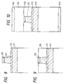
- an index antiguiding type semiconductor laser is constituted in which the top clad comprises a base layer formed on the active layer and a protrusion strip for current injection protruding from the base layer and comprising a second cladding layer made of AlGaInP.
- the semiconductor laser further comprises a light diffusion layer formed on the base layer adjacent to the protrusion strip and having an Al proportion smaller than that of AlGaInP of the second cladding layer and inclusive of zero, wherein the base layer has such a thickness as allows laser oscillation light to leak out to the light diffusion layer.
- the quantum well active layer 115 consists of a GaInP cladding layer 104, a GaInAsP optical confinement layer 105, a GaAs layer 106, a GaInAs quantum well layer 107, a GaAs layer 108, a GaInAsP optical confinement layer 109 and a GaInP cladding layer 110.
- the p-type AlGaInP cladding layer 111, p-type GaInP etching stopper layer 112, p-type AlGaInP cladding layer 113 and p-type GaInP cap layer constitutes a top clad.
- the p-type AlGaInP cladding layer 113 is shaped, by subsequent etching, into a protrusion strip that is coextensive and parallel with a current-injecting portion of the active layer.
Applications Claiming Priority (6)
| Application Number | Priority Date | Filing Date | Title |
|---|---|---|---|
| JP349280/92 | 1992-12-28 | ||
| JP34928092A JPH06204613A (ja) | 1992-12-28 | 1992-12-28 | 半導体レーザ |
| JP9438293 | 1993-04-21 | ||
| JP94382/93 | 1993-04-21 | ||
| JP188341/93 | 1993-07-29 | ||
| JP18834193A JPH077230A (ja) | 1993-04-21 | 1993-07-29 | 屈折率反導波型半導体レーザ |
Publications (2)
| Publication Number | Publication Date |
|---|---|
| EP0604965A1 true EP0604965A1 (de) | 1994-07-06 |
| EP0604965B1 EP0604965B1 (de) | 1997-09-10 |
Family
ID=27307531
Family Applications (1)
| Application Number | Title | Priority Date | Filing Date |
|---|---|---|---|
| EP93120981A Expired - Lifetime EP0604965B1 (de) | 1992-12-28 | 1993-12-27 | Halbleiterlaser mit Begrenzungsschicht aus AlGaInP |
Country Status (4)
| Country | Link |
|---|---|
| US (1) | US5586135A (de) |
| EP (1) | EP0604965B1 (de) |
| CA (1) | CA2112319C (de) |
| DE (1) | DE69313807T2 (de) |
Families Citing this family (6)
| Publication number | Priority date | Publication date | Assignee | Title |
|---|---|---|---|---|
| US5764671A (en) * | 1996-10-21 | 1998-06-09 | Motorola, Inc. | VCSEL with selective oxide transition regions |
| US6461884B1 (en) * | 2001-01-05 | 2002-10-08 | Manijeh Razeghi | Diode laser |
| JP2006245341A (ja) * | 2005-03-03 | 2006-09-14 | Mitsubishi Electric Corp | 半導体光素子 |
| JP2007250896A (ja) * | 2006-03-16 | 2007-09-27 | Sumitomo Electric Ind Ltd | 半導体光素子 |
| MX2011010622A (es) * | 2009-04-09 | 2012-02-23 | Folgers Coffee Co | Tableta de cafe tostado molido. |
| CN106384771B (zh) * | 2016-10-25 | 2019-01-11 | 华灿光电(浙江)有限公司 | AlGaInP基发光二极管外延片、芯片及制备方法 |
Citations (2)
| Publication number | Priority date | Publication date | Assignee | Title |
|---|---|---|---|---|
| JPH01181493A (ja) * | 1988-01-09 | 1989-07-19 | Sharp Corp | 端面窓型半導体レーザ素子 |
| JPH0439986A (ja) * | 1990-06-05 | 1992-02-10 | Fujitsu Ltd | 半導体レーザ装置 |
Family Cites Families (8)
| Publication number | Priority date | Publication date | Assignee | Title |
|---|---|---|---|---|
| GB2222307B (en) * | 1988-07-22 | 1992-04-01 | Mitsubishi Electric Corp | Semiconductor laser |
| US5146466A (en) * | 1988-09-29 | 1992-09-08 | Sanyo Electric Co., Ltd. | Semiconductor laser device |
| JPH04150087A (ja) * | 1990-10-12 | 1992-05-22 | Mitsubishi Electric Corp | 可視光半導体レーザ装置 |
| US5210767A (en) * | 1990-09-20 | 1993-05-11 | Mitsubishi Denki Kabushiki Kaisha | Semiconductor laser |
| US5274656A (en) * | 1991-06-12 | 1993-12-28 | Sumitomo Electric Industries, Ltd. | Semiconductor laser |
| JP3129779B2 (ja) * | 1991-08-30 | 2001-01-31 | 株式会社東芝 | 半導体レーザ装置 |
| JP3242967B2 (ja) * | 1992-01-31 | 2001-12-25 | 株式会社東芝 | 半導体発光素子 |
| US5222090A (en) * | 1992-03-05 | 1993-06-22 | Mcdonnell Douglas Corporation | 700-850 nanometer semiconductor diode laser |
-
1993
- 1993-12-23 CA CA002112319A patent/CA2112319C/en not_active Expired - Fee Related
- 1993-12-27 DE DE69313807T patent/DE69313807T2/de not_active Expired - Fee Related
- 1993-12-27 EP EP93120981A patent/EP0604965B1/de not_active Expired - Lifetime
- 1993-12-28 US US08/174,067 patent/US5586135A/en not_active Expired - Fee Related
Patent Citations (2)
| Publication number | Priority date | Publication date | Assignee | Title |
|---|---|---|---|---|
| JPH01181493A (ja) * | 1988-01-09 | 1989-07-19 | Sharp Corp | 端面窓型半導体レーザ素子 |
| JPH0439986A (ja) * | 1990-06-05 | 1992-02-10 | Fujitsu Ltd | 半導体レーザ装置 |
Non-Patent Citations (7)
| Title |
|---|
| I. KIDOGUCHI ET AL: "I-L characteristics of AlGaInP visible laser diode with lateral leaky waveguide structure", THE AUTUMN CONFERENCE OF THE JAPAN SOCIETY OF APPLIED PHYSICS, PAPER NO. 18A-V-5 1992, pages 952 * |
| I. YOSHIDA ET AL: "AlGaInP/GaInAs strained quantum well lasers", ELECTRONICS LETTERS., vol. 29, no. 8, 15 April 1993 (1993-04-15), STEVENAGE, HERTS, GB, pages 654 - 655 * |
| K. ITAYA ET AL: "Remarkable improvement in the Temperature characteristics of GaAs lasers using an InGaAlP cladding layer", CONFERENCE DIGEST, 13TH IEEE INTERNATIONAL SEMICONDUCTOR LASER CONFERENCE , SEPTEMBER 21-25 1992 TAKAMATSU, KAGAWA, JAPAN, PAPER M-5, pages 236 - 237 * |
| K. MOBARHAN ET AL: "GaInAs/GaAs/GaInP buried ridge structure single quantum well laser emitting at 0.98 mum", ELECTRONICS LETTERS., vol. 28, no. 16, 30 July 1992 (1992-07-30), STEVENAGE, HERTS, GB, pages 1510 - 1511 * |
| M.C. WU ET AL: "High temperature, high power InGaAs/GaAs Quantum well lasers with lattice matched InGaP Claddings", IEEE PHOTONICS TECHNOLOGY LETTERS, vol. 4, no. 7, July 1992 (1992-07-01), NEW YORK US, pages 676 - 679, XP000289282, DOI: doi:10.1109/68.145235 * |
| PATENT ABSTRACTS OF JAPAN vol. 13, no. 468 (E - 834) 23 October 1989 (1989-10-23) * |
| PATENT ABSTRACTS OF JAPAN vol. 16, no. 224 (E - 1206) 25 May 1992 (1992-05-25) * |
Also Published As
| Publication number | Publication date |
|---|---|
| CA2112319C (en) | 1999-01-05 |
| DE69313807D1 (de) | 1997-10-16 |
| DE69313807T2 (de) | 1998-01-22 |
| EP0604965B1 (de) | 1997-09-10 |
| US5586135A (en) | 1996-12-17 |
| CA2112319A1 (en) | 1994-06-29 |
Similar Documents
| Publication | Publication Date | Title |
|---|---|---|
| US4910743A (en) | Semiconductor laser with mesa stripe waveguide structure | |
| US6359919B1 (en) | Gallium nitride-based compound semiconductor laser and method of manufacturing the same | |
| US6049556A (en) | Vertical cavity surface emitting laser diode operable in 1.3 μm or 1.5 μm wavelength band with improved efficiency | |
| EP0259026B1 (de) | Doppelheterostruktur-Halbleiterlaser mit streifenförmigem Mesa-Wellenleiter | |
| EP1437809B1 (de) | Verbindungshalbleiterlaser | |
| EP0373933B1 (de) | Herstellungsverfahren für einen Halbleiterlaser mit nichtabsorbierender Spiegelstruktur | |
| US5336635A (en) | Manufacturing method of semiconductor laser of patterned-substrate type | |
| JP2555282B2 (ja) | 半導体レ−ザ装置及びその製造方法 | |
| US5963572A (en) | Semiconductor laser device and manufacturing method thereof | |
| US5586135A (en) | Semiconductor laser having an AlGaInP cladding layer | |
| US6697404B1 (en) | Laser diode operable in 1.3μm or 1.5μm wavelength band with improved efficiency | |
| EP0612128A2 (de) | Halbleiterlaser und Herstellungsverfahren | |
| KR0153585B1 (ko) | 메사 스트라이프 구조를 가진 반도체 레이저 및 그의 제조방법 | |
| JP2647076B2 (ja) | 半導体レーザ装置及びその製造方法 | |
| JP4028158B2 (ja) | 半導体光デバイス装置 | |
| JPH0815228B2 (ja) | 半導体レ−ザ装置及びその製造方法 | |
| KR20000035669A (ko) | 반도체 레이저, 반도체 장치 및 이들의 제조 방법 | |
| JPH10256647A (ja) | 半導体レーザ素子およびその製造方法 | |
| Yoshikawa et al. | A novel technology for formation of a narrow active layer in buried heterostructure lasers by single-step MOCVD | |
| EP1109231A2 (de) | Lichtemittierende Halbleitervorrichtung und Herstellungsverfahren | |
| JPH10135567A (ja) | 半導体レーザ素子 | |
| JP3146501B2 (ja) | 半導体レーザ及びその製造方法 | |
| JP2865160B2 (ja) | 半導体レーザの製造方法 | |
| EP1233492B1 (de) | Herstellungsverfahren für Verbindungshalbleiterlaser | |
| JP2780625B2 (ja) | 半導体レーザの製造方法 |
Legal Events
| Date | Code | Title | Description |
|---|---|---|---|
| PUAI | Public reference made under article 153(3) epc to a published international application that has entered the european phase |
Free format text: ORIGINAL CODE: 0009012 |
|
| AK | Designated contracting states |
Kind code of ref document: A1 Designated state(s): DE FR GB NL SE |
|
| 17P | Request for examination filed |
Effective date: 19940929 |
|
| 17Q | First examination report despatched |
Effective date: 19950418 |
|
| GRAG | Despatch of communication of intention to grant |
Free format text: ORIGINAL CODE: EPIDOS AGRA |
|
| GRAH | Despatch of communication of intention to grant a patent |
Free format text: ORIGINAL CODE: EPIDOS IGRA |
|
| GRAH | Despatch of communication of intention to grant a patent |
Free format text: ORIGINAL CODE: EPIDOS IGRA |
|
| GRAA | (expected) grant |
Free format text: ORIGINAL CODE: 0009210 |
|
| AK | Designated contracting states |
Kind code of ref document: B1 Designated state(s): DE FR GB NL SE |
|
| REF | Corresponds to: |
Ref document number: 69313807 Country of ref document: DE Date of ref document: 19971016 |
|
| ET | Fr: translation filed | ||
| PLBE | No opposition filed within time limit |
Free format text: ORIGINAL CODE: 0009261 |
|
| STAA | Information on the status of an ep patent application or granted ep patent |
Free format text: STATUS: NO OPPOSITION FILED WITHIN TIME LIMIT |
|
| 26N | No opposition filed | ||
| REG | Reference to a national code |
Ref country code: GB Ref legal event code: 746 Effective date: 19981009 |
|
| REG | Reference to a national code |
Ref country code: FR Ref legal event code: D6 |
|
| PGFP | Annual fee paid to national office [announced via postgrant information from national office to epo] |
Ref country code: SE Payment date: 19991207 Year of fee payment: 7 |
|
| PGFP | Annual fee paid to national office [announced via postgrant information from national office to epo] |
Ref country code: FR Payment date: 19991208 Year of fee payment: 7 |
|
| PGFP | Annual fee paid to national office [announced via postgrant information from national office to epo] |
Ref country code: GB Payment date: 19991222 Year of fee payment: 7 |
|
| PGFP | Annual fee paid to national office [announced via postgrant information from national office to epo] |
Ref country code: NL Payment date: 19991228 Year of fee payment: 7 |
|
| PGFP | Annual fee paid to national office [announced via postgrant information from national office to epo] |
Ref country code: DE Payment date: 19991230 Year of fee payment: 7 |
|
| PG25 | Lapsed in a contracting state [announced via postgrant information from national office to epo] |
Ref country code: GB Free format text: LAPSE BECAUSE OF NON-PAYMENT OF DUE FEES Effective date: 20001227 |
|
| PG25 | Lapsed in a contracting state [announced via postgrant information from national office to epo] |
Ref country code: SE Free format text: LAPSE BECAUSE OF NON-PAYMENT OF DUE FEES Effective date: 20001228 |
|
| PG25 | Lapsed in a contracting state [announced via postgrant information from national office to epo] |
Ref country code: NL Free format text: LAPSE BECAUSE OF NON-PAYMENT OF DUE FEES Effective date: 20010701 |
|
| EUG | Se: european patent has lapsed |
Ref document number: 93120981.1 |
|
| GBPC | Gb: european patent ceased through non-payment of renewal fee |
Effective date: 20001227 |
|
| PG25 | Lapsed in a contracting state [announced via postgrant information from national office to epo] |
Ref country code: FR Free format text: LAPSE BECAUSE OF NON-PAYMENT OF DUE FEES Effective date: 20010831 |
|
| NLV4 | Nl: lapsed or anulled due to non-payment of the annual fee |
Effective date: 20010701 |
|
| REG | Reference to a national code |
Ref country code: FR Ref legal event code: ST |
|
| PG25 | Lapsed in a contracting state [announced via postgrant information from national office to epo] |
Ref country code: DE Free format text: LAPSE BECAUSE OF NON-PAYMENT OF DUE FEES Effective date: 20011002 |