EP0601869B1 - Flat type display device and assembling method therefor - Google Patents
Flat type display device and assembling method therefor Download PDFInfo
- Publication number
- EP0601869B1 EP0601869B1 EP93309942A EP93309942A EP0601869B1 EP 0601869 B1 EP0601869 B1 EP 0601869B1 EP 93309942 A EP93309942 A EP 93309942A EP 93309942 A EP93309942 A EP 93309942A EP 0601869 B1 EP0601869 B1 EP 0601869B1
- Authority
- EP
- European Patent Office
- Prior art keywords
- conductor lines
- display
- scanning
- board
- conductor
- Prior art date
- Legal status (The legal status is an assumption and is not a legal conclusion. Google has not performed a legal analysis and makes no representation as to the accuracy of the status listed.)
- Expired - Lifetime
Links
Images


Classifications
-
- G—PHYSICS
- G09—EDUCATION; CRYPTOGRAPHY; DISPLAY; ADVERTISING; SEALS
- G09G—ARRANGEMENTS OR CIRCUITS FOR CONTROL OF INDICATING DEVICES USING STATIC MEANS TO PRESENT VARIABLE INFORMATION
- G09G3/00—Control arrangements or circuits, of interest only in connection with visual indicators other than cathode-ray tubes
- G09G3/20—Control arrangements or circuits, of interest only in connection with visual indicators other than cathode-ray tubes for presentation of an assembly of a number of characters, e.g. a page, by composing the assembly by combination of individual elements arranged in a matrix no fixed position being assigned to or needed to be assigned to the individual characters or partial characters
- G09G3/34—Control arrangements or circuits, of interest only in connection with visual indicators other than cathode-ray tubes for presentation of an assembly of a number of characters, e.g. a page, by composing the assembly by combination of individual elements arranged in a matrix no fixed position being assigned to or needed to be assigned to the individual characters or partial characters by control of light from an independent source
- G09G3/36—Control arrangements or circuits, of interest only in connection with visual indicators other than cathode-ray tubes for presentation of an assembly of a number of characters, e.g. a page, by composing the assembly by combination of individual elements arranged in a matrix no fixed position being assigned to or needed to be assigned to the individual characters or partial characters by control of light from an independent source using liquid crystals
- G09G3/3611—Control of matrices with row and column drivers
- G09G3/3674—Details of drivers for scan electrodes
- G09G3/3677—Details of drivers for scan electrodes suitable for active matrices only
-
- G—PHYSICS
- G02—OPTICS
- G02F—OPTICAL DEVICES OR ARRANGEMENTS FOR THE CONTROL OF LIGHT BY MODIFICATION OF THE OPTICAL PROPERTIES OF THE MEDIA OF THE ELEMENTS INVOLVED THEREIN; NON-LINEAR OPTICS; FREQUENCY-CHANGING OF LIGHT; OPTICAL LOGIC ELEMENTS; OPTICAL ANALOGUE/DIGITAL CONVERTERS
- G02F1/00—Devices or arrangements for the control of the intensity, colour, phase, polarisation or direction of light arriving from an independent light source, e.g. switching, gating or modulating; Non-linear optics
- G02F1/01—Devices or arrangements for the control of the intensity, colour, phase, polarisation or direction of light arriving from an independent light source, e.g. switching, gating or modulating; Non-linear optics for the control of the intensity, phase, polarisation or colour
- G02F1/13—Devices or arrangements for the control of the intensity, colour, phase, polarisation or direction of light arriving from an independent light source, e.g. switching, gating or modulating; Non-linear optics for the control of the intensity, phase, polarisation or colour based on liquid crystals, e.g. single liquid crystal display cells
- G02F1/133—Constructional arrangements; Operation of liquid crystal cells; Circuit arrangements
- G02F1/1333—Constructional arrangements; Manufacturing methods
- G02F1/1345—Conductors connecting electrodes to cell terminals
-
- G—PHYSICS
- G02—OPTICS
- G02F—OPTICAL DEVICES OR ARRANGEMENTS FOR THE CONTROL OF LIGHT BY MODIFICATION OF THE OPTICAL PROPERTIES OF THE MEDIA OF THE ELEMENTS INVOLVED THEREIN; NON-LINEAR OPTICS; FREQUENCY-CHANGING OF LIGHT; OPTICAL LOGIC ELEMENTS; OPTICAL ANALOGUE/DIGITAL CONVERTERS
- G02F1/00—Devices or arrangements for the control of the intensity, colour, phase, polarisation or direction of light arriving from an independent light source, e.g. switching, gating or modulating; Non-linear optics
- G02F1/01—Devices or arrangements for the control of the intensity, colour, phase, polarisation or direction of light arriving from an independent light source, e.g. switching, gating or modulating; Non-linear optics for the control of the intensity, phase, polarisation or colour
- G02F1/13—Devices or arrangements for the control of the intensity, colour, phase, polarisation or direction of light arriving from an independent light source, e.g. switching, gating or modulating; Non-linear optics for the control of the intensity, phase, polarisation or colour based on liquid crystals, e.g. single liquid crystal display cells
- G02F1/133—Constructional arrangements; Operation of liquid crystal cells; Circuit arrangements
- G02F1/136—Liquid crystal cells structurally associated with a semi-conducting layer or substrate, e.g. cells forming part of an integrated circuit
- G02F1/1362—Active matrix addressed cells
-
- G—PHYSICS
- G09—EDUCATION; CRYPTOGRAPHY; DISPLAY; ADVERTISING; SEALS
- G09G—ARRANGEMENTS OR CIRCUITS FOR CONTROL OF INDICATING DEVICES USING STATIC MEANS TO PRESENT VARIABLE INFORMATION
- G09G3/00—Control arrangements or circuits, of interest only in connection with visual indicators other than cathode-ray tubes
- G09G3/20—Control arrangements or circuits, of interest only in connection with visual indicators other than cathode-ray tubes for presentation of an assembly of a number of characters, e.g. a page, by composing the assembly by combination of individual elements arranged in a matrix no fixed position being assigned to or needed to be assigned to the individual characters or partial characters
- G09G3/34—Control arrangements or circuits, of interest only in connection with visual indicators other than cathode-ray tubes for presentation of an assembly of a number of characters, e.g. a page, by composing the assembly by combination of individual elements arranged in a matrix no fixed position being assigned to or needed to be assigned to the individual characters or partial characters by control of light from an independent source
- G09G3/36—Control arrangements or circuits, of interest only in connection with visual indicators other than cathode-ray tubes for presentation of an assembly of a number of characters, e.g. a page, by composing the assembly by combination of individual elements arranged in a matrix no fixed position being assigned to or needed to be assigned to the individual characters or partial characters by control of light from an independent source using liquid crystals
- G09G3/3611—Control of matrices with row and column drivers
- G09G3/3648—Control of matrices with row and column drivers using an active matrix
-
- G—PHYSICS
- G09—EDUCATION; CRYPTOGRAPHY; DISPLAY; ADVERTISING; SEALS
- G09G—ARRANGEMENTS OR CIRCUITS FOR CONTROL OF INDICATING DEVICES USING STATIC MEANS TO PRESENT VARIABLE INFORMATION
- G09G2310/00—Command of the display device
- G09G2310/02—Addressing, scanning or driving the display screen or processing steps related thereto
- G09G2310/0224—Details of interlacing
-
- G—PHYSICS
- G09—EDUCATION; CRYPTOGRAPHY; DISPLAY; ADVERTISING; SEALS
- G09G—ARRANGEMENTS OR CIRCUITS FOR CONTROL OF INDICATING DEVICES USING STATIC MEANS TO PRESENT VARIABLE INFORMATION
- G09G2310/00—Command of the display device
- G09G2310/02—Addressing, scanning or driving the display screen or processing steps related thereto
- G09G2310/0264—Details of driving circuits
- G09G2310/0286—Details of a shift registers arranged for use in a driving circuit
-
- G—PHYSICS
- G09—EDUCATION; CRYPTOGRAPHY; DISPLAY; ADVERTISING; SEALS
- G09G—ARRANGEMENTS OR CIRCUITS FOR CONTROL OF INDICATING DEVICES USING STATIC MEANS TO PRESENT VARIABLE INFORMATION
- G09G2310/00—Command of the display device
- G09G2310/06—Details of flat display driving waveforms
Definitions
- the present invention relates to a flat type display device employing liquid crystals, plasma, a thin film EL (Electro Luminescence), or the like driven through scanning of its display screen, such as a matrix type liquid crystal display device, and relates to a driving method and an assembling method for the display device.
- a flat type display device employing liquid crystals, plasma, a thin film EL (Electro Luminescence), or the like driven through scanning of its display screen, such as a matrix type liquid crystal display device, and relates to a driving method and an assembling method for the display device.
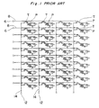
- Fig. 1 shows a conventional thin film transistor (TFT) matrix type liquid crystal display device.
- the liquid crystal display device is constructed by arranging in a matrix form unit cells each composed of a pixel P and a thin film transistor T one terminal of which is connected to the pixel P.
- the gates of the thin film transistors T, T, ... are connected to a scanning conductor line 8 in every row and the other terminals of the above-mentioned thin film transistors T, T, ... are connected to a display conductor line 14 in every column.
- Output signals at scanning signal output terminals 6, 6, ... of scanning drive LSI's (not shown) and output signals at display signal output terminals 12, 12, ... of display drive LSI's (not shown) are supplied to the scanning conductor lines 8, 8, ... and to the display conductor lines 14, 14, ...
- an output signal at one scanning signal output terminal 6 of a scanning signal is supplied to one scanning conductor line 8, as shown in Fig. 1. Therefore, for example, when 240 scanning conductor lines 8 are driven, the scanning drive LSI's are required to produce the same number of output signals, i.e., 240 output signals. In this case, when an LSI which produces 60 output signals is selected, four LSIs are to be provided. When an LSI which produces 80 output signals is selected, three LSIs are to be provided. When an LSI which produces 120 output signals is selected, two LSIs are to be provided.
- Fig. 2 shows another display device wherein ramification conductor lines A, B, C, and D, one end of each ramification conductor line being connected to a scanning signal output terminal 6 and the other end thereof ramifying into n branches, are provided, and a three-terminal transistors SW 11 to SW n4 are provided between the branches and corresponding scanning conductor lines G(1) through G(n) (Japanese Patent Publication No. 5-14915).
- the corresponding branches of the ramification conductor lines constitute a group, thus n groups of the branches are provided.
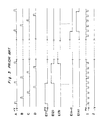
- Fig. 3 shows the waveforms of control signals for the display device shown in Fig. 2.
- the display device of Fig. 2 In the display device of Fig.
- n control conductor lines E(1) through E(n) connected to the gates of the transistors SW 11 - SW n4 are sequentially selected (electric potential is made to be positive (+V)) to sequentially select the groups of the branches, and the ramification conductor lines A, B, C, and D are sequentially selected when each group of the branches is selected to thereby select the corresponding scanning conductor lines in each group as shown in Fig. 3.
- the scanning conductor lines are selected group by group.
- transistors SW 11 to SW n4 are turned off, transistors P 1 through P N connected to the corresponding scanning conductor lines G(1) through G(N) are turned on (by signals I and J), and a constant voltage is applied to the scanning conductor lines G(1) through G(N) to achieve sufficient discharge of electricity.
- the number of connection terminals of the scanning line drive circuit 5 is smaller than the number of the scanning conductor lines G(1) through G(N).
- the resistance of the conductor lines made of a thin film increases, and therefore the conductor lines may catch noise to cause the malfunction of the display device or the deterioration of the display image quality.
- the scanning line drive circuit 5 and the signal line drive circuit 2 are arranged in two different directions with respect to the display board 1, two connection steps are required for the connection between the display board 1 and the drive circuit boards.
- a junction board 9 for transmitting timing signals and other signals must be provided, and therefore connection between the junction board and the drive circuit boards is required.
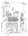
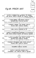
- Fig. 4 shows a display device assembling process where the display device shown in Fig. 2 is coupled with a junction board.
- connection material anisotropic conductive film or the like for connecting display conductor lines S(1) through S(M) on the display board (display panel) 1 with the signal line drive circuit 2 is supplied to either the display board 1 or to a signal line drive circuit board (not shown) (step S1).
- the signal line drive circuit board is placed adjacently along a side of the display board 1, that is, the signal line drive circuit board is aligned with the display board 1 (step S2). Then the signal line drive circuit board is connected with the display board so that the display conductor lines S(1) through S(M) on the display board 1 and output terminals of the signal line drive circuit 2 are connected with each other by way of the connection material (step S3). Then the display board 1 is turned by an angle of 90° (step S4).
- the ramification conductor lines A, B, C, and D, the control conductor lines E(1) through E(n), and the other conductor lines on the display board 1 are connected with output terminals of the scanning line drive circuit 5 by means of a connection material (steps S5 - S7). Then the display board 1 with the signal line drive circuit board and the scanning line drive circuit board is transferred (step S8).
- a connection material is supplied to either the junction board or the scanning line drive circuit board (step S9), alignment of both boards is performed (step S10), and conductor lines of the junction board are connected to the input terminals of the scanning line drive circuit 5 (step S11). Then the display board 1 in this condition is transferred (step S12).
- a connection material is supplied to either the junction board or the signal line drive circuit 2 (step S13), alignment of both boards is performed (step S14), and conductor lines of the junction board are connected to the input terminals of the signal line drive circuit 2 (step S15).
- the resulting module disadvantageously has a large size and heavy weight after assembling.
- the display device shown in Fig. 2 has many intersections of the conductor lines, which results in a reduced yield of the products.
- An object of the present invention is therefore to provide a display device and a driving method and an assembling method for the display device capable of reducing the number of drive LSIs to be employed without reducing the yield, simplifying the assembling procedure, achieving cost reduction, allowing a small-size light-weight construction of the module after assembling, and achieving a stable operation.
- Another object of the present invention is to produce a low-cost, high-reliability display device having a reduced number of drive LSIs and offering a high-definition display panel by utilizing conventional connection materials and conventional equipments.
- a further object of the present invention is to provide a device capable of remarkably increasing the display quality and reliability by avoiding any bad influence possibly exerted on drive elements at the time of instantaneous voltage drop of the scanning signal occurring when a video signal falls from a high level "H” to a low level "L".
- the present invention provides a display device in accordance with claim 1 as well as display device assembling methods in accordance with claims 22 and 24.
- the first ends of said ramification conductor lines are respectively connected to the scanning signal output terminals.
- the first switching elements are provided between the branches of said ramification conductor lines and the scanning conductor lines, and the conductor lines positioned between the cell units and the scanning signal output terminals bend substantially at a right angle toward the direction of the rows.
- the conductor lines that bend may be the ramification conductor lines or the scanning conductor lines. It should be noted that "bending of the ramification conductor line substantially at a right angle" includes a case wherein a branch thereof perpendicularly ramifies from the stem of the ramification conductor line.
- the output signal (output terminal) of the scanning drive LSI is ramified into a specified number of the branches to be supplied to the scanning conductor lines corresponding in number to the branches via the first switching elements.
- the scanning conductor lines corresponding in number to the branches are driven per output terminal of the scanning drive LSI. Therefore, the number of scanning drive LSIs to be employed can be reduced to a reciprocal of the number of branches, which leads to a remarkable cost reduction.
- the number of steps for connecting the junction board with the drive circuit board is reduced as the number of the drive circuit boards to be connected is reduced, which curtails the assembly procedure, when compared with a conventional case wherein drive circuit boards are connected with different sides of the display board.
- the reduction of the connection steps further reduces the cost as compared with the conventional case.
- the drive circuit board is provided along only a side of the display board, the resulting module has a small size and light weight.
- the branches of the ramification conductor lines constitute a plurality of groups, with the number of branches in each group being equal to the number of scanning signal output terminals; the nth group of branches comprises the nth branch of each ramification conductor line, where 1 ⁇ n ⁇ number of branches of each ramification conductor line; and, in each group of branches, the branches corresponding to the scanning signal output terminals are arranged in the same order as the output terminals.
- Each control conductor line may be commonly connected to the control terminals of the first switching elements connected to each group of the same n th branches of said ramification conductor lines.
- the scanning drive LSI generates successively a pulse output signal in a specified cycle at the scanning signal output terminals
- the control means generates on the control conductor line a control signal in synchronization with the output signal of the scanning drive LSI, said control signal having a cycle obtained by multiplying the cycle of the output signal of the scanning drive LSI by the number of the branches of one ramification conductor line to turn on and off the first switching elements group by group.
- Such an arrangement allows scanning of every group of the scanning conductor lines corresponding to the same n th branches of each ramification conductor line.
- a group of the first switching elements connected to the first branches of each ramification conductor line are turned on while the other first switching elements are turned off.
- the scanning conductor lines in the group corresponding to the first branch of each ramification conductor line are selected.
- the scanning conductor lines in the group are driven by the output signals of the scanning drive LSI.
- the first switching elements in a group connected to the second branches of each ramification conductor line are turned on while the other first switching elements are turned off so that the scanning conductor lines in the group corresponding to the second branches of each ramification conductor line are selected.
- the scanning conductor lines in the group are driven by the output signals of the scanning drive LSI.
- the first ends of said ramification conductor lines may be respectively connected to the display signal output terminals.
- the first switching elements may be provided between the branches of said ramification conductor lines and the display conductor lines, and the conductor lines positioned between the cell units and the display signal output terminals, more specifically either the ramification conductor lines or the display conductor lines, bend substantially at a right angle toward the direction of the columns.
- the branches of the ramification conductor lines constitute a plurality of groups, with the number of branches in each group being equal to the number of display signal output terminals; wherein the mth group of branches comprises the mth branch of each ramification conductor line, where 1 ⁇ m ⁇ number of branches of each ramification conductor line; and, in each group of branches, the branches corresponding to the display signal output terminals are arranged in the same order as the output terminals.
- each control conductor line may be commonly connected to the control terminals of the first switching elements connected to each group of the same m th branches of said ramification conductor lines. It will be easily understood that those arrangements can offer advantages similar to those obtained in the case that the first ends of said ramification conductor lines are connected to the scanning signal output terminals.
- the ramification conductor lines are connected to both the scanning signal output terminals and the display signal output terminals, the number of drive LSIs to be adopted can be further reduced.
- each of said unit cells comprises the pixel and a switching element, one terminal of which switching element is connected to the pixel and a control terminal of which switching element is connected to the scanning conductor line, and each scanning conductor line is connected to an external power terminal having a voltage sufficient to turn off the switching element of each unit cell via an off voltage supply line connected said external power terminal and a second switching element connected between said off-voltage supply line and the scanning conductor line, said second switching element being turned on and off by a control signal received at its control terminal.
- the control signal for turning on the second switching elements are continuously applied to the control terminals of the second switching elements when the first switching elements connected to the scanning conductor lines are turned off. Therefore, the electric charge on the scanning conductor lines is sufficiently discharged, with which the electric potential at the scanning conductor line is controlled to have a value for turning off the switching element of each unit cell. Therefore, a stable display operation is achieved.
- the switching element of each unit cell may be a thin film transistor or a thin film rectifying element.
- the second switching elements connected to the group of the adjacent scanning conductor lines may be connected to a common control conductor line at the control terminals thereof.
- the second switching elements are controlled to be turned on and off group by group. Therefore, a low operation frequency is achieved as compared with the transistors P 1 through P N shown in Fig. 2 to assure a stable operation of the display device.
- the first and second switching elements may be formed of thin film transistors or thin film rectifying elements. Then, the switching elements can be easily formed by an ordinary display device manufacturing process. Therefore, production of those switching elements does not increase the cost.
- a drive circuit board on which the scanning drive LSI and the display drive LSI are mounted is arranged adjacently along a side of the display board.
- the scanning signal output terminals of the scanning drive LSI and the display signal output terminals of the display drive LSI on said drive circuit board are connected with the corresponding conductor lines on said display board directly or by way of a junction board having substantially parallel conductor lines thereon. When they are directly connected, only one connection process is required to connect the display board with the drive circuit board, which leads to a simple assembly procedure.
- the present invention further reduces the production costs as compared with the conventional case. Furthermore, the drive circuit board and other components are provided along a side of the display board, the resulting module has a small size and light weight.
- the scanning drive LSI and display drive LSI may be provided on the display board, instead of being provided on the separate drive circuit board.
- each of the drive LSIs may have a power input terminal and a control signal input terminal
- a control board having conductor lines for supplying a power and a control signal to each of the drive LSIs may be arranged adjacently along a side of said display board, and the conductor lines on said control board may be connected with said input terminals of each of the drive LSIs or conductor lines formed on said display board and connected to said input terminals directly or by way of a junction board having substantially parallel conductor lines thereon.
- the control board and the junction board are connected with only one side of the display board, the assembly procedure becomes simpler. Therefore, the production costs are lower as compared with the conventional case.
- the control board and other components are provided along only one side of the display board, the resulting module has a small size and light weight.
- the display device where the scanning and display drive circuits are mounted on the drive circuit board can be assembled in the following manner.
- the drive circuit mounted with the drive LSIs is prepared, and a connection material for connecting the conductor lines of the display board with the output terminals of the drive LSIs is supplied to either the display board or the drive circuit board.
- the drive circuit board is arranged adjacently along the side of the display board, and the conductor lines on the display board are collectively connected with the respective output terminal on the drive circuit board by means of the connection material.
- the connection material may be supplied to the parallel conductor lines of the junction board.
- junction board and the drive circuit board are arranged adjacently along the side of the display board, and the conductor lines on the display board and the output terminals on the drive circuit board are collectively connected with the parallel conductor lines of the junction board by means of the connection material.
- the number of steps for assembly is fewer as compared with the conventional case.
- a display device of the present invention where the scanning and display drive circuits are mounted on the display board can be assembled in the following manner.
- a connection material for connecting the input terminals of each of the drive LSIs with the conductor lines for supplying a power and a control signal of the control board is supplied to the display board or the control board.
- the control board is arranged adjacently along a side of the display board, and the conductor lines on the control board are collectively connected with the input terminals of each of the drive LSIs or the conductor lines on the display board connected to the input terminals by means of the connection material.
- connection material is supplied to the parallel conductor lines of the junction board.
- the junction board and the control board are arranged adjacently along a side of the display board, and the conductor lines on the control board and the input terminals of each of the drive LSIs or the conductor lines on the display board connected to the input terminals are collectively connected with the parallel lines on the junction board by means of the connection material.
- the display device can be easily assembled in fewer steps as compared with the conventional case even when the junction board is interposed.
- Fig. 5 shows a TFT matrix type liquid crystal display device in accordance with an embodiment of the present invention.
- unit cells each composed of a pixel P and a thin film transistor T connected to the pixel P at one terminal are arranged in a matrix form on a display board 107.
- a thin film rectifying element may be used instead of the thin film transistor T.
- the gates of the thin film transistors T, T, ... in every row are connected to a scanning conductor line 108 extending in the direction of the row, while the other terminals of the thin film transistors T, T, ... in every column are connected to a display conductor line 114 extending in the direction of the column.
- a drive circuit board 118 on which a scanning drive LSI 122 and a display drive LSI 123 are mounted is provided adjacently along a side of the display board 107 intersecting perpendicularly to the display conductor lines 114.
- the above-mentioned display drive LSI 123 yields an output signal representing image data at its display signal output terminals 112, 112, ... arranged along a side adjacent to the display board 107 of the drive circuit board 118.
- the display conductor lines 114, 114, ... on the display board 107 are connected to the display signal output terminals 112, 112, ...
- the aforementioned scanning drive LSI 122 yields an output signal for scanning at its scanning signal output terminals 116a, 116b, 116c, 116d, 116e substantially aligned with the display signal output terminals 112, 112, ... on the drive circuit board 118.
- the scanning signal output terminals 116a - 116e are respectively connected to ends of ramification conductor lines 131, 132, 133, 134, and 135 provided on the display board 107.
- the ramification conductor lines 131 through 135 are arranged in the direction of the column on a side of the cell array, where the other ends of the ramification conductor lines 131 - 135 are respectively bifurcated into two branches 131a and 131b; 132a and 132b; 133a and 133b; 134a and 134b; and 135a and 135b.
- the ramification conductor lines 131-135 bend substantially at a right angle toward the scanning conductor lines 108. More specifically, the ramification conductor line branches 131a, 132a, 133a, 134a, 135a extend in the direction of the column by a specified length and bend at an angle of 90° to extend toward the corresponding rows of the cell array.
- the ramification conductor line branches 131b, 132b, 133b, 134b, 135b directly extend toward the corresponding rows of the cell array from the ramification points.
- the adjacent scanning conductor lines 108 of the number of the scanning signal output terminals (five in this case) constitute a group, and the adjacent scanning conductor lines of each group correspond to the same n th branches (0 ⁇ n ⁇ the number of the scanning signal output terminals) of the ramification conductor lines.
- n th branches 131a-135a; 131b-135b of said ramification conductor lines 131-135 constitute a group, and the branches 131a-135a; 131b-135b corresponding to the scanning signal output terminals in each group are disposed in the same order.
- the paired ramification conductor line branches 131a and 131b; ...; and 135a and 135b correspond to scanning conductor lines 108 and 108 in the rows separated apart from each other by the number (five in the present example) of the output signals of the scanning drive LSI 122.
- thin film transistors Q1, Q1#; Q2, Q2#; Q3, Q3#; Q4, Q4#; Q5 and Q5# are provided as first switching elements between the paired ramification conductor line branches 131a and 131b; ...; and 135a and 135b and the scanning conductor lines corresponding to the ramification conductor line branches.
- the gates of the thin film transistors Q1, Q2, ..., Q5 in a group are connected to a control conductor line 115a, while the gates of the thin film transistors Q1#, Q2#, ..., Q5# in another group are connected to a control conductor line 115b.
- the thin film transistors Q1-Q5, Q1#-Q5# of the two groups are controlled to be turned on and off alternately by control signals output to the control conductor lines 115a and 115b from control signal terminals 117a and 117b provided on the drive circuit board 118 as the control means.
- a circuit for generating the control signal (not shown) may be provided outside of the drive circuit board 118. Alternately such a circuit may be provided on the drive circuit board 118.
- Each of the control conductor lines 115a and 115b is a common bus line for each group of the thin film transistors Q1-Q5, Q1#-Q5#.
- the number of the thin film transistors Q1-Q5, Q1#-Q5# in each group is equal to the number of output signals of the scanning drive LSI. With this arrangement, the wiring space, that is, the space occupied by the conductor lines, is curtailed.
- the scanning drive LSI 123 In operation, the scanning drive LSI 123 generates pulse output signals in a constant cycle in a manner as shown in Fig. 6 and outputs them from the scanning signal output terminals 116a, 116b, ..., 116e. Meanwhile, from the control signal output terminals 117a and 117b are output the control signals which are synchronized with the output signal from the scanning signal output terminal 116a and have a cycle two (the number of branches) times greater than the cycle to turn on and off the thin film transistors Q1-Q5 and Q1#-Q5# in each group by turns. At the same time, the output signals (representing image data) at the output terminals 112 of the display drive LSI 122 are applied to the thin film transistors T of the unit cells via the display conductor lines 114. As a result, image display is performed.
- two scanning conductor lines 108 and 108 can be driven per output signal (output terminal) of the scanning drive LSI. Therefore, the number of scanning drive LSIs to be employed can be reduced to half that of the conventional case, which allows a remarkable cost reduction. Furthermore, it is unnecessary to make finer the pitch of the output terminals 116a-116e of the scanning drive LSI 123 or to increase the number of the output terminals per drive LSI, and therefore the yield is not reduced.
- the liquid crystal display device can be assembled in a simple and short process as shown in Fig. 9.
- a connection material for connecting the terminals 116a-116e, 117a, 117b, 112 of the drive circuit board 118 with the conductor lines 131-135, 115a, 115b, 114 of the display board (display panel) 107 is supplied to either of the boards 118 and 107 (step S1).
- the boards 118 and 107 are mutually aligned (step S2), and the boards 118 and 107 are connected so that the terminals of the boards 118 and 107 are connected with each other collectively by means of pressure welding or the like (step S3).
- the assembling can be performed in a very simple and short process as compared with the conventional case, which further reduces the cost.
- the drive circuit board 118 is provided along the side of the display board 107 perpendicular to the display conductor line 114, and the bent ramification conductor lines 131 - 135 and the thin film transistors Q1, Q1#; Q2, Q2#; Q3, Q3#; Q4, Q4#; Q5 and Q5# serving as the first switching elements are provided between the scanning conductor lines 108 and the scanning signal output terminals 116a - 116e in the example shown in Fig. 5, the present invention is not limited to the above-mentioned arrangement. For instance, as shown in Fig.
- one drive circuit board 118' may be provided along the side of the display board 107 perpendicular to the scanning conductor lines 108 and similar bent ramification conductor lines 131-133 having branches 131a-135a, 131b-135b and switching elements Q1-Q3, Q1#-Q3# may be provided between the display conductor lines 114 and the display signal output terminals 112a-112c.
- reference numeral 116 indicates a scanning signal output terminal.
- the adjacent display conductor lines 114 of the number of the display signal output terminals constitute a group, and the adjacent display conductor lines 114 of each group correspond to the same mth branches (0 ⁇ m ⁇ the number of the display signal output terminals) 131a-133a, 131b-133b of the ramification conductor lines.
- the same m th branches 131a-133a; 131b-133b of the ramification conductor lines constitute a group, and the branches corresponding to the display signal output terminals 112a-112c in each group are disposed in the same order.
- scanning drive LSI 122 and the display drive LSI 123 are not shown in Figs. 5A, 7 and 10 for the sake of simplification of the drawings. Furthermore, although only one scanning drive LSI 122 and only one display drive LSI 123 are shown in Fig. 5, it will be easily understood that more drive LSIs 122, 123 can be provided.
- ramification lines both between the scanning signal output terminals and the scanning conductor lines 108 and between the display signal output terminals and the display conductor lines 114.
- either the ramification conductor lines to be connected to the scanning conductor lines 108 or the ramification conductor lines to be connected with the display conductor lines 114 extend in the direction of the rows or the columns.
- thin film transistors U1, U2, U3, U4, U5, U1#, U2#, U3#, U4#, U5# are provided as second switching elements between the scanning conductor lines 108 and an off voltage supply line 110 connected to an external power terminal 111 having a voltage which sufficiently turns off the thin film transistor T of each unit cell as shown in Fig. 7.
- the electric potentials at control conductor lines 113a and 113b are controlled to turn on each of the above-mentioned thin film transistors U1-U5, U1#-U5# when the thin film transistors Q1-Q5, Q1#-Q5# are each off in correspondence with the electric potentials at the control conductor lines as shown in Fig. 8.
- the electric potentials at the scanning conductor lines 108 are stabilized when the thin film transistors Q1-Q5, Q1#-Q5# are off to allow the thin film transistor T of each unit cell to be sufficiently turned off.
- the present invention is not limited to such an arrangement. Unless the yield of connection is problematic, the number of branches can be increased to 3, 4 or more according which the number of scanning drive LSIs (or display drive LSIs) to be employed can be reduced to 1/3, 1/4 or less.
- the transistors can be easily formed in an ordinary liquid crystal display device manufacturing process. Therefore, the transistors can be provided without increasing the cost.
- the rectifying elements can be also easily formed in an ordinary liquid crystal display device manufacturing process, and therefore it does not increase the cost.
- Fig. 10 shows an example where a flexible wiring board 119 is interposed as a junction board between the display board 107 and the drive circuit board 118.
- the flexible wiring board 119 has substantially parallel conductor lines 120 to relay the output signals of each drive LSI.
- the drive circuit board 118 may be placed on a peripheral portion of the rear surface of the display board 107.
- the display device of Fig. 10 is produced as follows. After a connection material is supplied to the parallel conductor lines 120 of the junction board 119, the junction board 119 and the drive circuit board 118 are placed in position on one side of the display board 107. Then the parallel conductor lines 120 of the junction board 119 are collectively connected with both the conductor lines on the display board 107 and the output terminals on the drive circuit board 118 by means of the connection material. As is obvious, the number of steps for assembly is fewer as compared with the conventional case.
- the scanning drive LSI 122 and the display drive LSI 123 are not always required to form an external circuit of the display device.
- the scanning drive LSI 122 and the display drive LSI 123 may be provided on the display board 107, and powers and signals may be supplied to input terminals 124a, 124b, 124c, 125a, 125b, 125c of the drive LSIs 122 and 123 from a control board 121 having conductor lines 128, 129 for supplying powers and signals.
- the entire display device can be made compact.
- the display device as shown in Fig. 11 can be assembled in the following way. First, the display board 107 mounted with the drive circuits 122 and 123 and the control board 121 having the conductor lines 128, 129 are prepared. A connection material for connecting the input terminals 124a-124c, 125a-125c of each of the drive LSIs 122, 123 with the conductor lines 128, 129 is supplied to either the display board 107 or the control board 121.
- control board 121 is placed adjacently along a side of the display board 107, and the conductor lines 128, 129 on the control board 121 are collectively connected directly with the input terminals 124a-124c, 125a-125c of each of the drive LSIs 122, 123 or through the conductor lines 126, 127 on the display board connected to the input terminals 124a-124c, 125a-125c by means of the connection material.
- connection material is supplied to the parallel conductor lines 120 of the junction board 119. Then, after placing the junction board 119 and the control board 121 in position on one side of the display board 107, the conductor lines 128, 129 on the control board 121 and either the input terminals 124a-124c, 125a-125c of each of the drive LSIs 122, 123 or the conductor lines 126, 127 are collectively connected with the parallel lines 120 on the junction board 119 by the connection material.
- each output signal (output terminal) of either the scanning drive LSI or the display drive LSI is transmitted to a plurality of scanning conductor lines or display conductor lines by way of the corresponding ramification conductor line and first switching element. Therefore, the scanning conductor lines (or the display conductor lines) of the number corresponding to the number of the branches of one ramification conductor line are driven per output terminal of the scanning drive LSI or the display drive LSI. Therefore, the number of the scanning drive LSIs (or the display drive LSIs) to be employed is reduced by a factor equal to the number of the branches and is much smaller as compared with the conventional case to allow a remarkable cost reduction to be achieved.
- the yield is not reduced. Rather the yield increases because the connection portions of the drive LSIs are reduced in number as a whole. Furthermore, because the display signal output terminals and the scanning signal output terminals are arranged along a side of the display board, the display drive LSI and the scanning drive LSI can be mounted on a common drive circuit board along the side of the display board. When this arrangement is adopted, only one process is required for connecting the display board with the drive circuit board.
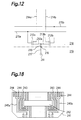
- Fig. 12 shows a schematic circuit diagram of a connection section between a display panel and a drive LSI of the display device in accordance with another embodiment of the present invention.
- a conductor line for sending one signal output from a drive LSI is bifurcated, and a switching element is provided for each branch.
- an output conductor line 217 connected to an output terminal 211 of the drive LSI formed on a flexible board 219 is connected via a connection portion 216 to a display panel board 218 to a ramification conductor line 213 formed on the display panel board 218 and ramified into two branches 213a and 213b at one end thereof.
- TFT thin film transistors
- Control conductor lines 215a and 215b for supplying individually to the gates of the TFTs 212a and 212b TFT control signals for controlling turning-on and turning-off of the TFTs are provided perpendicular to the signal transmission conductor lines 214a and 214b.
- the TFT 212a and the TFT 212b are alternately turned on and off to allow a signal from one output terminal 211 of the drive LSI to be transmitted alternately to the two signal transmission conductor lines 214a and 214b.
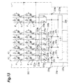
- Fig. 13 shows a schematic circuit diagram of a connection section between a TFT liquid crystal display panel and a drive LSI in the case where the assembly structure of the display device as shown in Fig. 12 is applied to a TFT liquid crystal display device. It should be noted that like components are denoted by the same reference numerals in Figs. 12 and 13.
- Output terminals 221A, 221B, 221C, ... of a drive LSI 220 formed on flexible board 219 are connected to connection portions 216A, 216B, 216C, ... for electrically connecting a liquid crystal display panel board 222 with the flexible board 219 by way of output conductor lines.
- the ramification conductor lines 213 connected to the connection portions 216A, 216B, 216C, ... on the side of the liquid crystal display panel board 222 are each ramified into two branches in the same manner as in Fig. 12. Between the branches and the scanning signal transmission conductor lines 223a and 223b are formed TFTs 212a and 212b which serve as switching elements.
- the control conductor lines 215a and 215b for supplying a TFT control signal individually to the gate electrodes of the TFTs 212a and 212b are provided perpendicularly to the scanning signal transmission conductor lines 223a and 223b. Ends of the control conductor line 215a and 215b are connected to control conductor lines 225a and 225b on the flexible board 219 via the connection portions 224a and 224b respectively.
- the pitch P1 of the connection portions 216A, 216B, 216C ... for connection between the liquid crystal display panel board 222 and the flexible board 219 is about twice as great as the pitch P2 of the scanning signal transmission conductor lines 223a, 223b, 223a, 223b, ... on the liquid crystal display panel board 222.
- Fig. 14 shows examples of waveforms of the TFT control signals for alternately turning on and off the TFTs 212a and 212b of the TFT liquid crystal display device shown in Fig. 13.
- a TFT control signal a is supplied to the control conductor line 225a shown in Fig. 13 to turn on the TFT 212a when the control signal has a high logic level "H" to allow a scanning signal to be transmitted to the scanning signal transmission conductor line 223a.
- a TFT control signal b is supplied to the control conductor line 225b to turn on the TFT 212b when the control signal has a high logic level "H" to allow a scanning signal to be transmitted to the scanning signal transmission conductor line 223b.
- the scanning signal transmission conductor lines 223a, 223a, ... are scanned in the first scanning time in response to the scanning signals A, B, C, ... output from output terminals 221A, 221B, 221C, ... of the drive LSI 220, and the scanning signal transmission conductor lines 223b, 223b, ... are scanned in the second scanning time.
- Fig. 15 shows an example of a pattern around the connection portion between the liquid crystal display panel board 222 and the flexible board 219 shown in Fig. 13.
- connection terminal (a first connection terminal) of the output conductor line 217 and a connection terminal (a second connection terminal) of the ramification conductor line 213 on the side of the liquid crystal display panel board 222 are mutually aligned and connected with each other by direct pressure welding using an anisotropic conductive film, solder, photo-setting resin, clip, or the like or another method to form the aforementioned connection portion 216.
- connection portion is defined as a portion where two corresponding connection terminals are connected with each other.
- the ramification conductor lines 213 are each ramified into two branches 213a and 213b on the side of the scanning signal transmission conductor lines 223.
- the output conductor line 217 connected to the output terminal 221 of the drive LSI 220 on the flexible board 219 is connected to the ramification conductor line 213 on the liquid crystal display panel board 222 via the connection portion 216.
- the TFTs 212a and 212b are alternately turned on and off by the TFT control signals alternately supplied to the gate electrodes of the TFTs from the control conductor line 215a or the control conductor line 215b. Therefore, a scanning signal from one output terminal 221 of the drive LSI 220 can be transmitted alternately to the two scanning signal transmission conductor lines 223a and 223b on the liquid crystal display panel board 222.
- the conventional flexible board with the LSIs and the conventional connection methods can be used.
- the conventional connection material such as the anisotropic conductive film and the conventional equipment for connection can be used.
- the liquid crystal display panel board 222 and the flexible board 219 are required to be connected with each other at twice as large a pinch as the pitch of the scanning signal transmission conductor lines 223 formed on the liquid crystal display panel board 222. Therefore, the pitch of the connection portions 216 can be set wide enough to remarkably improve the reliability of the connection between the liquid crystal display panel board 222 and the flexible board 219.
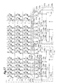
- Fig. 16 shows a circuit diagram of a variant of the TFT liquid crystal display device shown in Fig. 13 to which the assembly structure of the display device as shown in Fig. 12 is applied. It should be noted that like components are denoted by the same reference numerals in Figs. 13 and 16, and no description therefor is provided below.
- the flexible board 219 has control conductor lines 225a and 225b whose connection terminals (third connection terminals) are connected via the connection portions 224a and 224b to connection terminals (fourth connection terminals) of the control conductor lines 215a and 215b respectively for supplying a TFT control signal individually to the gate electrodes of the TFTs 212a and 212b.
- control conductor lines denoted now by 232a and 232b, are formed on a circuit board 231 provided separately from the flexible board 219.
- Fig. 17 shows a circuit diagram of another embodiment where the assembly structure of the display device as shown in Fig. 12 is applied to a TFT liquid crystal display device. It should be noted that like components are denoted by the same reference numerals in Figs. 13, 16 and 17 and no description therefor is provided below.
- the TFT liquid crystal display panel is driven by the scanning signals from a plurality of drive LSIs (only two 220, 234 of which are shown).
- the drive LSIs 220, 234 are formed on respective exclusive-use flexible boards 219, 233 having the same configuration.
- the control conductor lines 215a and 215b for supplying the TFT control signals individually to the gate electrodes of the TFTs 212a and 212b are connected to the control conductor lines 225a and 225b formed on the flexible board 219 via the connection portions 224a and 224b in the same manner as in Fig. 13.
- the control conductor lines 215a and 215b are not connected to the control conductor lines 238a, 238b by providing unconnected portions 237a and 237b.
- Fig. 18 shows an example of a wiring pattern of the flexible board 219 provided with the control conductor lines to be connected to the control conductor lines 215a and 215b on the liquid crystal display panel board 222 via the connection sections 224a and 224b.
- a flexible board 241 being on the market or already existing is formed with a drive LSI 242, and a plurality of auxiliary terminal patterns (or dummy terminal patterns) 244, 244, ... are provided for the output signal conductor line patterns 243, 243, ... from the drive LSI 242.
- control conductor line patterns 245a and 245b (corresponding to the control conductor lines 225a and 225b shown in Figs. 13 and 17) for supplying the TFT control signals to the gate electrodes of the TFTs 212a and 212b are formed on the flexible board 241 by utilizing the auxiliary terminal patterns (or the dummy terminal patterns) 244.
- the assembly structure of the display device of the invention can be achieved by utilizing the conventional connection material and the conventional connection equipment as they are.
- Fig. 19 is a circuit diagram of the vicinity of a connection section between a TFT liquid crystal display panel and a scanning electrode drive LSI in accordance with a modification of the example shown in Fig. 17. It should be noted that in Figs. 17 and 19 like components are denoted by the same reference numerals and no description therefor is provided below.
- control conductor lines 215a and 215b for supplying the TFT control signals individually to the gate electrodes of the TFTs 212a and 212b are connected to the control conductor lines 225a and 225b formed on the flexible board 219 via the connection portions 224a and 224b in the same manner as in Fig. 17.
- the control conductor lines 238a and 238b on the other flexible boards are not used. Therefore unnecessary areas (X) and (Y) on which the control conductor lines 238a and 238b are formed are removed from the other flexible boards 233.
- control conductor lines 225a and 225b By forming the control conductor lines 225a and 225b only on one flexible board 219 and removing the unnecessary areas (X) and (Y) from the flexible boards 233 as described above, the flexible boards become light in weight and each module can be designed to be compact.
- the removal of the areas (X) and (Y) from the flexible boards 233, ... can be performed when a continuous flexible board having a plurality of sets of the conductor lines of the same pattern is, after getting mounted with a plurality of the drive LSIs in position, subjected to a blanking process for dividing the continuous flexible board into a plurality of individual flexible boards.
- a conventional flexible board manufacturing procedure is arranged to include a first blanking (or cutting) process in which the areas (X) and (Y) are reserved and a second blanking (or cutting) process in which the areas (X) and (Y) are removed from an individual flexible board.
- the continuous flexible board is subjected to either the first blanking (or cutting) process or the second blanking (or cutting) process for each purpose.
- this method can utilize a conventional flexible board manufacturing procedure.
- Fig. 20 is a circuit diagram of a connection section between the TFT liquid crystal display panel and the scanning electrode drive LSI in an embodiment where the TFT control signals supplied to the TFTs 212a and 212b is generated by a TFT control signal generating circuit formed inside the drive LSI. It should be noted that in Figs. 13 and 20 like components are denoted by the same reference numerals and no description therefor is provided here.
- the control conductor lines 215a and 215b for supplying the TFT control signals to the gate electrodes of the TFTs 212a and 212b are connected to the control conductor lines 251a and 251b formed on the flexible board 219 via the connection portions 224a and 224b.
- the respective other ends of the control conductor lines 251a and 251b are connected to output terminals 252a and 252b of the TFT control signal generating circuit (not shown) formed inside the drive LSI 220.
- the TFT control signal generating circuit is provided inside the drive LSI 220, less design change is required for a control board externally provided, and yet it is possible to achieve the same effect as produced by the assembly structure of the TFT liquid crystal display device.
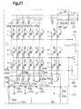
- Fig. 21 shows a modification of the embodiment shown in Fig. 13.
- an electric potential at the scanning signal transmission conductor line (e.g., scanning signal transmission conductor line 223a) connected to the TFT being not selected (e.g., TFT 212a) may become unstable, which may cause the pixels connected to the scanning signal transmission conductor line (e.g., scanning signal transmission conductor line 223a) to exhibit a faulty display image.
- a stabilizing power is supplied to the scanning signal transmission conductor lines 223a and 223b from a connection portion 260 via a power line 261 and TFTs 262a and 262b.
- the TFTs 262b are controlled to be turned on and off by the TFT control signal supplied to the TFTs 262b from the connection portion 263 via a control conductor line 265, while the TFTs 262a are controlled to be turned on and off by the TFT control signal supplied to the TFT 262a from a connection section 264 via a control conductor line 266, whereby the stabilizing power is supplied to the unselected scanning signal transmission conductor line 223a or scanning signal transmission conductor line 223b.
- the above-mentioned TFTs 262a and 262b may be provided adjacent to the TFTs 212a and 212b. However, in the present embodiment, the TFTs 262a and 262b are provided at the side opposite from the side where the TFTs 212a and 212b are provided. By so doing, the time during which the TFT T connected to the pixel P is supplied with the scanning signal can be as short as possible, whereby the scanning signal can be stably supplied thereto.
- conductor lines 269 and 270 for externally supplying the TFT control signals to the above-mentioned control conductor lines 265 and 266 as well as a conductor line 271 for externally supplying the stabilizing power to the power line 261 are provided on a flexible board 268 on which a drive LSI 267 for supplying a display signal to each TFT constituting each pixel on the liquid crystal display panel board 222.
- the conductor lines 269, 270, and 271 can be collectively connected with the control conductor lines 265 and 266 and the power line 261 by way of the connection portions 263, 264, and 260. Furthermore, there is no need to prepare any additional flexible board for the conductor lines 269, 270, and 271, which allows reduction in number of parts.
- Fig. 22 shows an active-matrix display device in accordance with a comparative example.
- a transparent insulating board 302 which is made of glass and which has a laterally elongated rectangular shape are provided a plurality of gate lines 307 serving as scanning conductor lines and a plurality of source lines 308 serving as signal lines perpendicularly intersecting the gate lines 307.
- the gate lines 307 are arranged in the horizontal direction, while the source lines 308 are arranged in the vertical direction.
- pixels 303 In the areas surrounded by the gate lines 307 and the source lines 308 are provided pixels 303 in a matrix form. At the intersections between the gate lines 307 and the source lines 308 are provided thin film transistors 304 serving as switching elements.
- a gate line drive element 305 extending in the widthwise direction, where the gate line drive element 305 is connected to an end of each of the gate lines 307.
- a source line drive element 306 extending in the lengthwise direction, where the source line drive element 306 is connected to an end of each of the source lines 308. It should be noted that the gate line drive element 305 and the source line drive element 306 are practically provided on the transparent insulating board pattern by the COG (Chip On Glass) connection method.
- the gate line drive element 305 is connected to a plurality of input terminal lines 310.
- the gate line drive element 305 sequentially scans the gate lines 307 in the vertical direction while the source line drive element 306 applies a video signal to a source line 308 to write the signal line by line to thereby make the active-matrix display device perform an image display operation.
- Portions of the transparent insulating board 302 except for the portions where the gate line drive element 305 and the source line drive element 306 are provided serve as a display section 301.
- interruption thin film transistors 309 serving as switching elements to make and break a connection between them.
- the gate electrodes of the interruption thin film transistors 309 are connected to an interruption signal input terminal 316 formed on the transparent insulating board 302 in a position slightly apart toward an end of the board 302 from the aforementioned input terminal lines 310, and an interruption control signal 313 is input from an external control circuit (not shown) via the interruption signal input terminal 316.
- FIG. 23 shows the waveforms of a video signal 311 supplied to the source lines 308, a scanning signal 312 given to the gate lines 307, and an interruption control signal 313 input to the interruption signal input terminal 316 for the interruption thin film transistor 309, respectively.
- (d) shows the waveform of a certain signal inside the gate line drive element 305.
- the interruption thin film transistor 309 is provided to prevent the possible bad influence of an instantaneous voltage drop 315 attributed to the change in level from "H" to "L” of the video signal 311 supplied to the source lines 308 from being exerted on the gate line drive element 305.
- the interruption control signal 313 having the waveform shown in (c) is given to the interruption signal input terminal 316 for the interruption thin film transistors 309 temporarily in synchronization with the fall from "H" to "L” of the video signal 311 in the example of Figure 22. While the control signal 313 is given, the interruption thin film transistors 309 are off to open the connection between the gate lines 307 and the gate line drive element 305, i.e., temporarily electrically disconnect the gate lines 307 from the gate line drive element 305.
- the interruption thin film transistor 309 is on to connect the gate line drive element 305 with the gate lines 307.
- the instantaneous voltage drop 315 at the gate lines will be transmitted to the gate line drive element 305 and affect various signals (represented by the signal 314) therein so that a momentary change of voltage takes place to the signal 314 as shown in Fig. 26.
- the gate line drive element 305 neither malfunctions nor is subjected to total breakdown due to a voltage exceeding its endurance voltage. Furthermore, since no momentary change of voltage due to the instantaneous voltage drop takes place, a great voltage difference between the "on" voltage and the "off" voltage for the thin film transistor 304 is ensured within the range of the endurance voltage of the gate line drive element 305. The voltage difference is sufficient to easily improve the display quality.
- an active-matrix display device having the gate lines always electrically connected with the gate line drive element is formed by the COG connection method, a resistance combined with the connection resistance and the resistance of the patterned conductor lines on the display board will be exerted on the input terminal lines 310 of the gate line drive element 305 and enlarge the momentary change of voltage due to the instantaneous voltage drop 315.
- the gate lines 307 are designed to be electrically disconnected from the gate line drive element 305 when the instantaneous voltage drop 315 occurs, the instantaneous voltage drop 315 is not transmitted to the gate line drive element 305 and the voltage change of the signal 314 in the gate line drive element 305 as shown in Fig. 26 is avoided.
- Fig. 24 shows an active-matrix display device in accordance with another comparative example.
- the present example takes the measure of avoiding the condition where the thin film transistors 304 are not sufficiently turned off due to the possible instability of the electric potential at the gate lines 307 when the gate lines 307 are electrically disconnected from the gate line drive element 305 by the operation of the interruption thin film transistors 309.
- the following describes the detail of the construction. It should be noted that the construction of most of the parts is similar to that in Figs. 22, and therefore like components are denoted by the same reference numerals in Figs. 22 and 24 and no further description on those components is provided here.
- each gate line signal switching thin film transistor 317 is connected to a control signal input terminal 319 provided at a portion adjacent to the interruption signal input terminal 316 on the transparent insulating board 302, and a power switching control signal 320 (see Fig. 25 (e)) is input via the control signal input terminal 319 from an external circuit.
- each switching thin film transistor 317 is connected to the thin film transistor 304, while the drain electrode thereof is connected to an external power input terminal 318.
- the external power input terminal 318 is formed in a position slightly apart from the input terminal line 310 at the opposite side from the interruption signal input terminal 316 and control signal input terminal 319, and an OFF voltage signal 321 is input via the external power input terminal 318 from an external power source.
- the signal 320 is given to the gate electrode of the switching thin film transistor 317 at the time as shown in Fig. 25, i.e., when the video signal 311 falls from "H” to "L” and an interruption control signal 314 at an OFF level is input to the interruption thin film transistors 309.
- an OFF voltage 321 is given to the thin film transistors 304 via the external power input terminal 318 and the switching thin film transistors 317.
- an OFF voltage to sufficiently turn transistors off is supplied to the thin film transistors 304 when the gate lines 307 are made to be electrically disconnected from the gate line drive element 305 by the operation of the interruption thin film transistors 309. Therefore, the insufficient turning off of the thin film transistors 304 due to the unstable electric potential at the gate lines 307 can be securely prevented.
- the present invention can be also applied to the case where a TAB (Tape Automated Bonding) drive element is formed by the COF (Chip On Film) method or to the case where a drive element is formed on a glass board.
- TAB Pear Automated Bonding
- COF Chip On Film
- the thin film transistor to be used in the present invention is typically an insulated gate field effect transistor using amorphous silicon, polysilicon, Te, or the like as a semiconductor material.
- the active-matrix display device of the present invention can be applied not only to a monochrome liquid crystal display device but also to a color liquid crystal display device employing a color filter.
- the various signals inside the scanning conductor line drive element can be kept stable, and therefore the possible malfunction or breakdown of the element due to a voltage exceeding the endurance voltage of the scanning conductor line drive element can be securely prevented. Furthermore, the momentary change of voltage attributed to the instantaneous voltage drop does not takes place, and therefore a great voltage difference can be assured between the "on" voltage and the "off" voltage of the first switching element within the range of the endurance voltage of the gate line drive element.
- the present invention can provide a high-quality, high-reliability active-matrix display device.
- the active-matrix display device shown in Fig. 25 can further improve the reliability, because the first switching elements 304 are prevented from being insufficiently turned off due to the instability of the electric potential at the gate lines while the connection between the scanning conductor lines and the scanning conductor line drive element is undone.
Landscapes
- Physics & Mathematics (AREA)
- Engineering & Computer Science (AREA)
- Nonlinear Science (AREA)
- Crystallography & Structural Chemistry (AREA)
- General Physics & Mathematics (AREA)
- Chemical & Material Sciences (AREA)
- Computer Hardware Design (AREA)
- Theoretical Computer Science (AREA)
- Mathematical Physics (AREA)
- Optics & Photonics (AREA)
- Microelectronics & Electronic Packaging (AREA)
- Liquid Crystal (AREA)
- Liquid Crystal Display Device Control (AREA)
- Control Of Indicators Other Than Cathode Ray Tubes (AREA)
- Devices For Indicating Variable Information By Combining Individual Elements (AREA)
Description
- The present invention relates to a flat type display device employing liquid crystals, plasma, a thin film EL (Electro Luminescence), or the like driven through scanning of its display screen, such as a matrix type liquid crystal display device, and relates to a driving method and an assembling method for the display device.
- Fig. 1 shows a conventional thin film transistor (TFT) matrix type liquid crystal display device. The liquid crystal display device is constructed by arranging in a matrix form unit cells each composed of a pixel P and a thin film transistor T one terminal of which is connected to the pixel P. The gates of the thin film transistors T, T, ... are connected to a
scanning conductor line 8 in every row and the other terminals of the above-mentioned thin film transistors T, T, ... are connected to adisplay conductor line 14 in every column. Output signals at scanningsignal output terminals signal output terminals scanning conductor lines display conductor lines - In general, an output signal at one scanning
signal output terminal 6 of a scanning signal is supplied to onescanning conductor line 8, as shown in Fig. 1. Therefore, for example, when 240 scanningconductor lines 8 are driven, the scanning drive LSI's are required to produce the same number of output signals, i.e., 240 output signals. In this case, when an LSI which produces 60 output signals is selected, four LSIs are to be provided. When an LSI which produces 80 output signals is selected, three LSIs are to be provided. When an LSI which produces 120 output signals is selected, two LSIs are to be provided. - Lately, flat type display devices such as a liquid crystal display are in keen underselling competition, and therefore cost reduction has been a serious problem. Among others, the drive LSIs (scanning drive LSIs and display drive LSIs) are expensive, and form a great part of the total cost of the liquid crystal display device, and therefore the LSIs are the key parts for cost reduction.
- In view of the above-mentioned fact, there have been trials to reduce chip size by making finer the pitch of output terminals or to increase the number of output terminals per drive LSI to reduce the number of LSIs for the purpose of reducing the costs of the drive LSIs. However, none of the above-mentioned trials have been able to achieve sufficient cost reduction, rather, it is possible to lower the yield and reliability because a lot of terminals must be connected at a fine pitch on the board of the liquid crystal display device. The above-mentioned fact is common to devices such as a simple-matrix display device where its display signal system is scanned by means of a drive LSI.
- Fig. 2 shows another display device wherein ramification conductor lines A, B, C, and D, one end of each ramification conductor line being connected to a scanning
signal output terminal 6 and the other end thereof ramifying into n branches, are provided, and a three-terminal transistors SW11 to SWn4 are provided between the branches and corresponding scanning conductor lines G(1) through G(n) (Japanese Patent Publication No. 5-14915). The corresponding branches of the ramification conductor lines constitute a group, thus n groups of the branches are provided. Fig. 3 shows the waveforms of control signals for the display device shown in Fig. 2. In the display device of Fig. 2, n control conductor lines E(1) through E(n) connected to the gates of the transistors SW11 - SWn4 are sequentially selected (electric potential is made to be positive (+V)) to sequentially select the groups of the branches, and the ramification conductor lines A, B, C, and D are sequentially selected when each group of the branches is selected to thereby select the corresponding scanning conductor lines in each group as shown in Fig. 3. With the above-mentioned operation, the scanning conductor lines are selected group by group. Meanwhile, when the transistors SW11 to SWn4 are turned off, transistors P1 through PN connected to the corresponding scanning conductor lines G(1) through G(N) are turned on (by signals I and J), and a constant voltage is applied to the scanning conductor lines G(1) through G(N) to achieve sufficient discharge of electricity. - In the display device shown in Fig. 2, the number of connection terminals of the scanning
line drive circuit 5 is smaller than the number of the scanning conductor lines G(1) through G(N). However, since the whole length of the conductor lines arranged between the scanningline drive circuit 5 and adisplay board 1 are long, the resistance of the conductor lines made of a thin film increases, and therefore the conductor lines may catch noise to cause the malfunction of the display device or the deterioration of the display image quality. - Furthermore, in the display device shown in Fig. 2, since the scanning
line drive circuit 5 and the signalline drive circuit 2 are arranged in two different directions with respect to thedisplay board 1, two connection steps are required for the connection between thedisplay board 1 and the drive circuit boards. When occasion demands, ajunction board 9 for transmitting timing signals and other signals must be provided, and therefore connection between the junction board and the drive circuit boards is required. - Fig. 4 shows a display device assembling process where the display device shown in Fig. 2 is coupled with a junction board.
- First, a connection material (anisotropic conductive film or the like) for connecting display conductor lines S(1) through S(M) on the display board (display panel) 1 with the signal
line drive circuit 2 is supplied to either thedisplay board 1 or to a signal line drive circuit board (not shown) (step S1). - Then the signal line drive circuit board is placed adjacently along a side of the
display board 1, that is, the signal line drive circuit board is aligned with the display board 1 (step S2). Then the signal line drive circuit board is connected with the display board so that the display conductor lines S(1) through S(M) on thedisplay board 1 and output terminals of the signalline drive circuit 2 are connected with each other by way of the connection material (step S3). Then thedisplay board 1 is turned by an angle of 90° (step S4). - In the same manner as described above, the ramification conductor lines A, B, C, and D, the control conductor lines E(1) through E(n), and the other conductor lines on the
display board 1 are connected with output terminals of the scanningline drive circuit 5 by means of a connection material (steps S5 - S7). Then thedisplay board 1 with the signal line drive circuit board and the scanning line drive circuit board is transferred (step S8). - Subsequently, a connection material is supplied to either the junction board or the scanning line drive circuit board (step S9), alignment of both boards is performed (step S10), and conductor lines of the junction board are connected to the input terminals of the scanning line drive circuit 5 (step S11). Then the
display board 1 in this condition is transferred (step S12). In the same manner as described above, a connection material is supplied to either the junction board or the signal line drive circuit 2 (step S13), alignment of both boards is performed (step S14), and conductor lines of the junction board are connected to the input terminals of the signal line drive circuit 2 (step S15). As described above, there are problematically many processes for the assembling (note that the alignment process at step S14 can be eliminated). - As is evident from the above, the assembling procedure has a lot of steps and is troublesome to result in cost increase.
- Furthermore, since the conductor lines A-D, E(1)-E(n), and I and J occupy a wide non-display area on the display board and also since the circuit extends in two directions with respect to the display screen, the resulting module disadvantageously has a large size and heavy weight after assembling.
- Furthermore, since the operation frequencies of the transistors P1 through PN are high, they possibly operate faultily.
- Furthermore, the display device shown in Fig. 2 has many intersections of the conductor lines, which results in a reduced yield of the products.
- An object of the present invention is therefore to provide a display device and a driving method and an assembling method for the display device capable of reducing the number of drive LSIs to be employed without reducing the yield, simplifying the assembling procedure, achieving cost reduction, allowing a small-size light-weight construction of the module after assembling, and achieving a stable operation.
- Another object of the present invention is to produce a low-cost, high-reliability display device having a reduced number of drive LSIs and offering a high-definition display panel by utilizing conventional connection materials and conventional equipments.
- A further object of the present invention is to provide a device capable of remarkably increasing the display quality and reliability by avoiding any bad influence possibly exerted on drive elements at the time of instantaneous voltage drop of the scanning signal occurring when a video signal falls from a high level "H" to a low level "L".
- In order to accomplish these objects, the present invention provides a display device in accordance with
claim 1 as well as display device assembling methods in accordance with claims 22 and 24. - In an embodiment, the first ends of said ramification conductor lines are respectively connected to the scanning signal output terminals. In this case, the first switching elements are provided between the branches of said ramification conductor lines and the scanning conductor lines, and the conductor lines positioned between the cell units and the scanning signal output terminals bend substantially at a right angle toward the direction of the rows. The conductor lines that bend may be the ramification conductor lines or the scanning conductor lines. It should be noted that "bending of the ramification conductor line substantially at a right angle" includes a case wherein a branch thereof perpendicularly ramifies from the stem of the ramification conductor line.
- In this display device, the output signal (output terminal) of the scanning drive LSI is ramified into a specified number of the branches to be supplied to the scanning conductor lines corresponding in number to the branches via the first switching elements. As a result, the scanning conductor lines corresponding in number to the branches are driven per output terminal of the scanning drive LSI. Therefore, the number of scanning drive LSIs to be employed can be reduced to a reciprocal of the number of branches, which leads to a remarkable cost reduction. Furthermore, it is neither necessary to make finer the pitch of the output terminals of the drive LSI nor to increase the number of the output terminals per drive LSI, and therefore the yield is not reduced. Rather the yield increases because the connection portions of the drive LSIs are reduced in number as a whole. Furthermore, since the conductor lines positioned between the cell units and the scanning signal output terminals, specifically, either the ramification conductor lines or the scanning conductor lines, bend substantially at a right angle toward the direction of the rows, the scanning signal output terminals are arranged on a line extending from the array of the display signal output terminals along a side of the display board. Therefore, the display drive LSI and the scanning drive LSI can be mounted on the same drive circuit board along a side of the display board. When the above-mentioned arrangement is adopted, only one connection process is required to connect the display board with the drive circuit board, which leads to a simple assembly procedure. When a junction board is provided to transmit a timing signal and other signals, the number of steps for connecting the junction board with the drive circuit board is reduced as the number of the drive circuit boards to be connected is reduced, which curtails the assembly procedure, when compared with a conventional case wherein drive circuit boards are connected with different sides of the display board. The reduction of the connection steps further reduces the cost as compared with the conventional case. Furthermore, since the drive circuit board is provided along only a side of the display board, the resulting module has a small size and light weight.
- In an embodiment, the branches of the ramification conductor lines constitute a plurality of groups, with the number of branches in each group being equal to the number of scanning signal output terminals; the nth group of branches comprises the nth branch of each ramification conductor line, where 1 ≤ n ≤ number of branches of each ramification conductor line; and, in each group of branches, the branches corresponding to the scanning signal output terminals are arranged in the same order as the output terminals.
- Each control conductor line may be commonly connected to the control terminals of the first switching elements connected to each group of the same nth branches of said ramification conductor lines. In this display device, the scanning drive LSI generates successively a pulse output signal in a specified cycle at the scanning signal output terminals, and the control means generates on the control conductor line a control signal in synchronization with the output signal of the scanning drive LSI, said control signal having a cycle obtained by multiplying the cycle of the output signal of the scanning drive LSI by the number of the branches of one ramification conductor line to turn on and off the first switching elements group by group. Such an arrangement allows scanning of every group of the scanning conductor lines corresponding to the same nth branches of each ramification conductor line. For example, a group of the first switching elements connected to the first branches of each ramification conductor line are turned on while the other first switching elements are turned off. With this operation, the scanning conductor lines in the group corresponding to the first branch of each ramification conductor line are selected. In this condition, the scanning conductor lines in the group are driven by the output signals of the scanning drive LSI. Then the first switching elements in a group connected to the second branches of each ramification conductor line are turned on while the other first switching elements are turned off so that the scanning conductor lines in the group corresponding to the second branches of each ramification conductor line are selected. In this condition, the scanning conductor lines in the group are driven by the output signals of the scanning drive LSI. Thus many scanning conductor lines are successively driven by a relatively small number of output signals. Therefore, the number of scanning drive LSIs and therefore the costs can be remarkably reduced as compared with the conventional case. Furthermore, because the common control conductor lines are used, it is possible to reduce a wiring space, that is, a space occupied by the conductor lines.
- The first ends of said ramification conductor lines may be respectively connected to the display signal output terminals. In this case, the first switching elements may be provided between the branches of said ramification conductor lines and the display conductor lines, and the conductor lines positioned between the cell units and the display signal output terminals, more specifically either the ramification conductor lines or the display conductor lines, bend substantially at a right angle toward the direction of the columns.
- In an embodiment, the branches of the ramification conductor lines constitute a plurality of groups, with the number of branches in each group being equal to the number of display signal output terminals; wherein the mth group of branches comprises the mth branch of each ramification conductor line, where 1 ≤ m ≤ number of branches of each ramification conductor line; and, in each group of branches, the branches corresponding to the display signal output terminals are arranged in the same order as the output terminals.
And, each control conductor line may be commonly connected to the control terminals of the first switching elements connected to each group of the same mth branches of said ramification conductor lines. It will be easily understood that those arrangements can offer advantages similar to those obtained in the case that the first ends of said ramification conductor lines are connected to the scanning signal output terminals. - If the ramification conductor lines are connected to both the scanning signal output terminals and the display signal output terminals, the number of drive LSIs to be adopted can be further reduced.
- According to an embodiment of the present invention, each of said unit cells comprises the pixel and a switching element, one terminal of which switching element is connected to the pixel and a control terminal of which switching element is connected to the scanning conductor line, and each scanning conductor line is connected to an external power terminal having a voltage sufficient to turn off the switching element of each unit cell via an off voltage supply line connected said external power terminal and a second switching element connected between said off-voltage supply line and the scanning conductor line, said second switching element being turned on and off by a control signal received at its control terminal. In the display device, the control signal for turning on the second switching elements are continuously applied to the control terminals of the second switching elements when the first switching elements connected to the scanning conductor lines are turned off. Therefore, the electric charge on the scanning conductor lines is sufficiently discharged, with which the electric potential at the scanning conductor line is controlled to have a value for turning off the switching element of each unit cell. Therefore, a stable display operation is achieved.
- The switching element of each unit cell may be a thin film transistor or a thin film rectifying element.
- The second switching elements connected to the group of the adjacent scanning conductor lines may be connected to a common control conductor line at the control terminals thereof. In this case, the second switching elements are controlled to be turned on and off group by group. Therefore, a low operation frequency is achieved as compared with the transistors P1 through PN shown in Fig. 2 to assure a stable operation of the display device.
- The first and second switching elements may be formed of thin film transistors or thin film rectifying elements. Then, the switching elements can be easily formed by an ordinary display device manufacturing process. Therefore, production of those switching elements does not increase the cost.
- In an embodiment of the invention, a drive circuit board on which the scanning drive LSI and the display drive LSI are mounted is arranged adjacently along a side of the display board. The scanning signal output terminals of the scanning drive LSI and the display signal output terminals of the display drive LSI on said drive circuit board are connected with the corresponding conductor lines on said display board directly or by way of a junction board having substantially parallel conductor lines thereon. When they are directly connected, only one connection process is required to connect the display board with the drive circuit board, which leads to a simple assembly procedure. Even though they are connected by way of the junction board having the substantially parallel conductor lines to transmit a timing signal or other signals, the number of connection steps for connecting the junction board with the drive circuit board is reduced as compared with the conventional case, since the drive circuit board is placed only on one side of the display board. Therefore, the present invention further reduces the production costs as compared with the conventional case. Furthermore, the drive circuit board and other components are provided along a side of the display board, the resulting module has a small size and light weight.
- The scanning drive LSI and display drive LSI may be provided on the display board, instead of being provided on the separate drive circuit board. In this case, each of the drive LSIs may have a power input terminal and a control signal input terminal, a control board having conductor lines for supplying a power and a control signal to each of the drive LSIs may be arranged adjacently along a side of said display board, and the conductor lines on said control board may be connected with said input terminals of each of the drive LSIs or conductor lines formed on said display board and connected to said input terminals directly or by way of a junction board having substantially parallel conductor lines thereon. Because the control board and the junction board are connected with only one side of the display board, the assembly procedure becomes simpler. Therefore, the production costs are lower as compared with the conventional case. Furthermore, the control board and other components are provided along only one side of the display board, the resulting module has a small size and light weight.
- The display device according to the above embodiments of the present invention where the scanning and display drive circuits are mounted on the drive circuit board can be assembled in the following manner. First, the drive circuit mounted with the drive LSIs is prepared, and a connection material for connecting the conductor lines of the display board with the output terminals of the drive LSIs is supplied to either the display board or the drive circuit board. Then, the drive circuit board is arranged adjacently along the side of the display board, and the conductor lines on the display board are collectively connected with the respective output terminal on the drive circuit board by means of the connection material. When the junction board is used, the connection material may be supplied to the parallel conductor lines of the junction board. The junction board and the drive circuit board are arranged adjacently along the side of the display board, and the conductor lines on the display board and the output terminals on the drive circuit board are collectively connected with the parallel conductor lines of the junction board by means of the connection material. As is obvious, the number of steps for assembly is fewer as compared with the conventional case.
- On the other hand, a display device of the present invention where the scanning and display drive circuits are mounted on the display board can be assembled in the following manner. A connection material for connecting the input terminals of each of the drive LSIs with the conductor lines for supplying a power and a control signal of the control board is supplied to the display board or the control board. The control board is arranged adjacently along a side of the display board, and the conductor lines on the control board are collectively connected with the input terminals of each of the drive LSIs or the conductor lines on the display board connected to the input terminals by means of the connection material.
- When the junction board is used, the connection material is supplied to the parallel conductor lines of the junction board. The junction board and the control board are arranged adjacently along a side of the display board, and the conductor lines on the control board and the input terminals of each of the drive LSIs or the conductor lines on the display board connected to the input terminals are collectively connected with the parallel lines on the junction board by means of the connection material. As is obvious, the display device can be easily assembled in fewer steps as compared with the conventional case even when the junction board is interposed.
- The present invention will become more fully understood from the detailed description given hereinbelow and the accompanying drawings which are given by way of illustration only, and thus are not limitative of the present invention, and wherein:
- Fig. 1 is a diagram showing a display section of a conventional active-matrix type liquid crystal display device;
- Fig. 2 is a circuit diagram showing the construction of another conventional active-matrix type liquid crystal display device;
- Fig. 3 is a timing chart of control signals of the liquid crystal display device shown in Fig. 2;
- Fig. 4 is a flow chart of the assembly process of the liquid crystal display device shown in Fig. 2;
- Fig. 5 is a circuit diagram of an active-matrix type liquid crystal display device in accordance with an embodiment of the present invention;
- Fig. 5A is a circuit diagram of another embodiment of the display device of the present invention;
- Fig. 6 is a timing chart of control signals of the display device shown in Fig. 5;
- Fig. 7 is a diagram showing a modified example of the display device of Fig. 5;
- Fig. 8 is a timing chart of control signals of the display device of Fig. 7;
- Fig. 9 is a flow chart of the assembly process of the display device of Fig. 5;
- Fig. 10 is a circuit diagram of a display device according to an embodiment of the present invention;
- Fig. 11 is a circuit diagram of a liquid crystal display device according to an embodiment of the present invention;
- Fig. 12 is a schematic circuit diagram illustrating a connection structure between a display panel and a drive LSI for a display device according to the present invention;
- Fig. 13 is a circuit diagram of a TFT liquid crystal display device to which the connection structure of Fig. 12 is applied;
- Fig. 14 is a timing chart of TFT control signals for alternately turning on and off the TFTs shown in Fig. 13;
- Fig. 15 is a diagram showing a pattern of the connection portion shown in Fig. 13;
- Fig. 16 is a circuit diagram of another TFT liquid crystal display device to which the connection structure of Fig. 12 is applied;
- Fig. 17 is a circuit diagram of another TFT liquid crystal display device to which the connection structure of Fig. 12 is applied;
- Fig. 18 is an exemplified wiring pattern of a flexible board of the examples shown in Figs. 13 and 17;
- Fig. 19 is a circuit diagram of another TFT liquid crystal display device to which the connection structure of Fig. 12 is applied;
- Fig. 20 is a circuit diagram of another TFT liquid crystal display device to which the connection structure of Fig. 12 is applied;
- Fig. 21 is a diagram showing a modified example of the connection structure between the TFT liquid crystal display panel and the scanning electrode drive LSI shown in Fig. 13;
- Fig. 22 is a circuit diagram of an active-matrix display device;
- Fig. 23 is a timing chart showing the timing of turning on and off various signals in the active-matrix display device shown in Fig. 22;
- Fig. 24 is a circuit diagram of an active-matrix display device; and
- Fig. 25 is a timing chart showing the timing of turning on and off various signals in the active-matrix display device shown in Fig. 24; and
- Fig. 26 is a timing chart for explaining a problem caused by the instantaneous voltage drop of a scanning signal.
-
- Fig. 5 shows a TFT matrix type liquid crystal display device in accordance with an embodiment of the present invention. In the present liquid crystal display device, unit cells each composed of a pixel P and a thin film transistor T connected to the pixel P at one terminal are arranged in a matrix form on a
display board 107. A thin film rectifying element may be used instead of the thin film transistor T. The gates of the thin film transistors T, T, ... in every row are connected to ascanning conductor line 108 extending in the direction of the row, while the other terminals of the thin film transistors T, T, ... in every column are connected to adisplay conductor line 114 extending in the direction of the column. Further adrive circuit board 118 on which ascanning drive LSI 122 and adisplay drive LSI 123 are mounted is provided adjacently along a side of thedisplay board 107 intersecting perpendicularly to the display conductor lines 114. The above-mentioneddisplay drive LSI 123 yields an output signal representing image data at its displaysignal output terminals display board 107 of thedrive circuit board 118. Thedisplay conductor lines display board 107 are connected to the displaysignal output terminals scanning drive LSI 122 yields an output signal for scanning at its scanningsignal output terminals signal output terminals drive circuit board 118. The scanningsignal output terminals 116a - 116e are respectively connected to ends oframification conductor lines display board 107. Theramification conductor lines 131 through 135 are arranged in the direction of the column on a side of the cell array, where the other ends of the ramification conductor lines 131 - 135 are respectively bifurcated into twobranches conductor line branches conductor line branches scanning conductor lines 108 of the number of the scanning signal output terminals (five in this case) constitute a group, and the adjacent scanning conductor lines of each group correspond to the same nth branches (0 < n ≤ the number of the scanning signal output terminals) of the ramification conductor lines. The samen th branches 131a-135a; 131b-135b of said ramification conductor lines 131-135 constitute a group, and thebranches 131a-135a; 131b-135b corresponding to the scanning signal output terminals in each group are disposed in the same order. In other words, the paired ramificationconductor line branches scanning conductor lines scanning drive LSI 122. Further, thin film transistors Q1, Q1#; Q2, Q2#; Q3, Q3#; Q4, Q4#; Q5 and Q5# are provided as first switching elements between the paired ramificationconductor line branches control conductor line 115a, while the gates of the thin film transistors Q1#, Q2#, ..., Q5# in another group are connected to acontrol conductor line 115b. The thin film transistors Q1-Q5, Q1#-Q5# of the two groups are controlled to be turned on and off alternately by control signals output to thecontrol conductor lines control signal terminals drive circuit board 118 as the control means. A circuit for generating the control signal (not shown) may be provided outside of thedrive circuit board 118. Alternately such a circuit may be provided on thedrive circuit board 118. Each of thecontrol conductor lines - In operation, the
scanning drive LSI 123 generates pulse output signals in a constant cycle in a manner as shown in Fig. 6 and outputs them from the scanningsignal output terminals signal output terminals signal output terminal 116a and have a cycle two (the number of branches) times greater than the cycle to turn on and off the thin film transistors Q1-Q5 and Q1#-Q5# in each group by turns. At the same time, the output signals (representing image data) at theoutput terminals 112 of thedisplay drive LSI 122 are applied to the thin film transistors T of the unit cells via the display conductor lines 114. As a result, image display is performed. - Thus in the present liquid crystal display device, two
scanning conductor lines output terminals 116a-116e of thescanning drive LSI 123 or to increase the number of the output terminals per drive LSI, and therefore the yield is not reduced. - Furthermore, the liquid crystal display device can be assembled in a simple and short process as shown in Fig. 9. In more detail, firstly a connection material for connecting the
terminals 116a-116e, 117a, 117b, 112 of thedrive circuit board 118 with the conductor lines 131-135, 115a, 115b, 114 of the display board (display panel) 107 is supplied to either of theboards 118 and 107 (step S1). Then theboards boards boards - Although the
drive circuit board 118 is provided along the side of thedisplay board 107 perpendicular to thedisplay conductor line 114, and the bent ramification conductor lines 131 - 135 and the thin film transistors Q1, Q1#; Q2, Q2#; Q3, Q3#; Q4, Q4#; Q5 and Q5# serving as the first switching elements are provided between thescanning conductor lines 108 and the scanningsignal output terminals 116a - 116e in the example shown in Fig. 5, the present invention is not limited to the above-mentioned arrangement. For instance, as shown in Fig. 5A, one drive circuit board 118' may be provided along the side of thedisplay board 107 perpendicular to thescanning conductor lines 108 and similar bent ramification conductor lines 131-133 havingbranches 131a-135a, 131b-135b and switching elements Q1-Q3, Q1#-Q3# may be provided between thedisplay conductor lines 114 and the display signal output terminals 112a-112c. In Fig. 5A,reference numeral 116 indicates a scanning signal output terminal. In the case of the example of Fig. 5A, the adjacentdisplay conductor lines 114 of the number of the display signal output terminals (three in this case) constitute a group, and the adjacentdisplay conductor lines 114 of each group correspond to the same mth branches (0 < m ≤ the number of the display signal output terminals) 131a-133a, 131b-133b of the ramification conductor lines. Thesame mth branches 131a-133a; 131b-133b of the ramification conductor lines constitute a group, and the branches corresponding to the display signal output terminals 112a-112c in each group are disposed in the same order. - It is to be noted that the
scanning drive LSI 122 and thedisplay drive LSI 123 are not shown in Figs. 5A, 7 and 10 for the sake of simplification of the drawings. Furthermore, although only onescanning drive LSI 122 and only onedisplay drive LSI 123 are shown in Fig. 5, it will be easily understood thatmore drive LSIs - Furthermore, it is possible to provide ramification lines both between the scanning signal output terminals and the
scanning conductor lines 108 and between the display signal output terminals and the display conductor lines 114. In this case, either the ramification conductor lines to be connected to thescanning conductor lines 108 or the ramification conductor lines to be connected with thedisplay conductor lines 114 extend in the direction of the rows or the columns. - In the example shown in Fig. 5, when the thin film transistors Q1-Q5, Q1#-Q5# are off, the electric potential at the
scanning conductor line 108 sometimes becomes unstable to insufficiently turn off the thin film transistor T of each unit cell. In such a case, as shown in Fig. 7, thin film transistors U1, U2, U3, U4, U5, U1#, U2#, U3#, U4#, U5# are provided as second switching elements between thescanning conductor lines 108 and an off voltage supply line 110 connected to anexternal power terminal 111 having a voltage which sufficiently turns off the thin film transistor T of each unit cell as shown in Fig. 7. Then the electric potentials atcontrol conductor lines scanning conductor lines 108 are stabilized when the thin film transistors Q1-Q5, Q1#-Q5# are off to allow the thin film transistor T of each unit cell to be sufficiently turned off. - Although the ramification conductor lines 131 - 135 are each bifurcated in the embodiments described as above, the present invention is not limited to such an arrangement. Unless the yield of connection is problematic, the number of branches can be increased to 3, 4 or more according which the number of scanning drive LSIs (or display drive LSIs) to be employed can be reduced to 1/3, 1/4 or less.
- Since the first and second switching elements Q1-Q5, Q1#-Q5#, U1-U5, U1#-U5# are composed of thin film transistors, the transistors can be easily formed in an ordinary liquid crystal display device manufacturing process. Therefore, the transistors can be provided without increasing the cost. When the first and second switching elements are made of thin film rectifying elements, the rectifying elements can be also easily formed in an ordinary liquid crystal display device manufacturing process, and therefore it does not increase the cost.
- Fig. 10 shows an example where a
flexible wiring board 119 is interposed as a junction board between thedisplay board 107 and thedrive circuit board 118. Theflexible wiring board 119 has substantiallyparallel conductor lines 120 to relay the output signals of each drive LSI. In order to reduce the external dimensions of the resulting module, thedrive circuit board 118 may be placed on a peripheral portion of the rear surface of thedisplay board 107. - The display device of Fig. 10 is produced as follows. After a connection material is supplied to the
parallel conductor lines 120 of thejunction board 119, thejunction board 119 and thedrive circuit board 118 are placed in position on one side of thedisplay board 107. Then theparallel conductor lines 120 of thejunction board 119 are collectively connected with both the conductor lines on thedisplay board 107 and the output terminals on thedrive circuit board 118 by means of the connection material. As is obvious, the number of steps for assembly is fewer as compared with the conventional case. - Furthermore, the
scanning drive LSI 122 and thedisplay drive LSI 123 are not always required to form an external circuit of the display device. As shown in Fig. 11, thescanning drive LSI 122 and thedisplay drive LSI 123 may be provided on thedisplay board 107, and powers and signals may be supplied to inputterminals drive LSIs control board 121 havingconductor lines - The display device as shown in Fig. 11 can be assembled in the following way. First, the
display board 107 mounted with thedrive circuits control board 121 having theconductor lines input terminals 124a-124c, 125a-125c of each of thedrive LSIs conductor lines display board 107 or thecontrol board 121. Then thecontrol board 121 is placed adjacently along a side of thedisplay board 107, and theconductor lines control board 121 are collectively connected directly with theinput terminals 124a-124c, 125a-125c of each of thedrive LSIs conductor lines input terminals 124a-124c, 125a-125c by means of the connection material. - When the
junction board 119 having theparallel conductor lines 120 is interposed between thedisplay board 107 and thecontrol board 121, although such an example is not shown, the connection material is supplied to theparallel conductor lines 120 of thejunction board 119. Then, after placing thejunction board 119 and thecontrol board 121 in position on one side of thedisplay board 107, theconductor lines control board 121 and either theinput terminals 124a-124c, 125a-125c of each of thedrive LSIs conductor lines parallel lines 120 on thejunction board 119 by the connection material. - As is evident from the above description, according to the display device of the present invention, each output signal (output terminal) of either the scanning drive LSI or the display drive LSI is transmitted to a plurality of scanning conductor lines or display conductor lines by way of the corresponding ramification conductor line and first switching element. Therefore, the scanning conductor lines (or the display conductor lines) of the number corresponding to the number of the branches of one ramification conductor line are driven per output terminal of the scanning drive LSI or the display drive LSI. Therefore, the number of the scanning drive LSIs (or the display drive LSIs) to be employed is reduced by a factor equal to the number of the branches and is much smaller as compared with the conventional case to allow a remarkable cost reduction to be achieved. Furthermore, since the above arrangement neither makes finer the pitch of the output terminals of the drive LSI nor increases the number of output terminals per drive LSI, the yield is not reduced. Rather the yield increases because the connection portions of the drive LSIs are reduced in number as a whole. Furthermore, because the display signal output terminals and the scanning signal output terminals are arranged along a side of the display board, the display drive LSI and the scanning drive LSI can be mounted on a common drive circuit board along the side of the display board. When this arrangement is adopted, only one process is required for connecting the display board with the drive circuit board.
- Fig. 12 shows a schematic circuit diagram of a connection section between a display panel and a drive LSI of the display device in accordance with another embodiment of the present invention. According to the assembly structure of the display device of the present embodiment, a conductor line for sending one signal output from a drive LSI is bifurcated, and a switching element is provided for each branch.
- Referring to Fig. 12, an
output conductor line 217 connected to anoutput terminal 211 of the drive LSI formed on aflexible board 219 is connected via aconnection portion 216 to adisplay panel board 218 to aramification conductor line 213 formed on thedisplay panel board 218 and ramified into twobranches - Between the
branches transmission conductor lines branches Control conductor lines TFTs transmission conductor lines - With the above-mentioned arrangement, by supplying the TFT control signals alternately to the
control conductor line 215a and thecontrol conductor line 215b, theTFT 212a and theTFT 212b are alternately turned on and off to allow a signal from oneoutput terminal 211 of the drive LSI to be transmitted alternately to the two signaltransmission conductor lines - Fig. 13 shows a schematic circuit diagram of a connection section between a TFT liquid crystal display panel and a drive LSI in the case where the assembly structure of the display device as shown in Fig. 12 is applied to a TFT liquid crystal display device. It should be noted that like components are denoted by the same reference numerals in Figs. 12 and 13.
-
Output terminals drive LSI 220 formed onflexible board 219 are connected toconnection portions display panel board 222 with theflexible board 219 by way of output conductor lines. - The
ramification conductor lines 213 connected to theconnection portions display panel board 222 are each ramified into two branches in the same manner as in Fig. 12. Between the branches and the scanning signaltransmission conductor lines TFTs control conductor lines TFTs transmission conductor lines control conductor line conductor lines flexible board 219 via theconnection portions - As is evident from Fig. 13, the pitch P1 of the
connection portions display panel board 222 and theflexible board 219 is about twice as great as the pitch P2 of the scanning signaltransmission conductor lines display panel board 222. - Fig. 14 shows examples of waveforms of the TFT control signals for alternately turning on and off the
TFTs control conductor line 225a shown in Fig. 13 to turn on theTFT 212a when the control signal has a high logic level "H" to allow a scanning signal to be transmitted to the scanning signaltransmission conductor line 223a. Meanwhile, a TFT control signal b is supplied to thecontrol conductor line 225b to turn on theTFT 212b when the control signal has a high logic level "H" to allow a scanning signal to be transmitted to the scanning signaltransmission conductor line 223b. - Therefore, by inverting the levels of the TFT control signals a and b in correspondence with the cycles of scanning signals A, B, C, ... as shown in Fig. 14 output from the
output terminals aforementioned drive LSI 220, the scanning signaltransmission conductor lines output terminals drive LSI 220, and the scanning signaltransmission conductor lines - In other words, twice as many scanning signal transmission conductor lines as the number of scanning signals output from the
drive LSI 220 can be scanned. Therefore, by increasing the number of branches of theramification conductor line 213 connected to the scanning signal output terminal of thedrive LSI 220 to three, four, or more, it is possible to scan three, four, or more times as many scanning signal transmission conductor lines as the scanning signal transmission conductor lines used in the conventional case. - Fig. 15 shows an example of a pattern around the connection portion between the liquid crystal
display panel board 222 and theflexible board 219 shown in Fig. 13. - Referring to Fig. 15, a connection terminal (a first connection terminal) of the
output conductor line 217 and a connection terminal (a second connection terminal) of theramification conductor line 213 on the side of the liquid crystaldisplay panel board 222 are mutually aligned and connected with each other by direct pressure welding using an anisotropic conductive film, solder, photo-setting resin, clip, or the like or another method to form theaforementioned connection portion 216. In the following description, the "connection portion" is defined as a portion where two corresponding connection terminals are connected with each other. - The
ramification conductor lines 213 are each ramified into twobranches - According to the assembly structure of the display device of the present embodiment shown in Figs. 12-15, the
output conductor line 217 connected to the output terminal 221 of thedrive LSI 220 on theflexible board 219 is connected to theramification conductor line 213 on the liquid crystaldisplay panel board 222 via theconnection portion 216. Between thebranches ramification conductor line 213 and the scanning signaltransmission conductor lines TFTs TFT 212a and theTFT 212b are alternately turned on and off by the TFT control signals alternately supplied to the gate electrodes of the TFTs from thecontrol conductor line 215a or thecontrol conductor line 215b. Therefore, a scanning signal from one output terminal 221 of thedrive LSI 220 can be transmitted alternately to the two scanning signaltransmission conductor lines display panel board 222. - In other words, the present embodiment can achieve a display device assembly structure which on one hand can significantly reduce the number of drive LSIs required to be used for driving the liquid crystal display panel, when compared with the conventional assembly structure and which on the other hand can make finer the liquid crystal display panel (which means increase of the number of pixels P = reduction of the pixel pitch) without reducing the pitch of the output terminals of the drive LSIs or increasing the number of the drive LSIs. According to the present display device assembly structure, the conventional flexible board with the LSIs and the conventional connection methods can be used. Also, the conventional connection material such as the anisotropic conductive film and the conventional equipment for connection can be used. Thus, neither investment for development of new methods and materials nor investment for new equipments is required. As a result, a superior display device assembly structure is achieved at a low cost.
- Furthermore, according to the present embodiment, the liquid crystal
display panel board 222 and theflexible board 219 are required to be connected with each other at twice as large a pinch as the pitch of the scanning signal transmission conductor lines 223 formed on the liquid crystaldisplay panel board 222. Therefore, the pitch of theconnection portions 216 can be set wide enough to remarkably improve the reliability of the connection between the liquid crystaldisplay panel board 222 and theflexible board 219. - Fig. 16 shows a circuit diagram of a variant of the TFT liquid crystal display device shown in Fig. 13 to which the assembly structure of the display device as shown in Fig. 12 is applied. It should be noted that like components are denoted by the same reference numerals in Figs. 13 and 16, and no description therefor is provided below.
- In the embodiment of Fig. 13, the
flexible board 219 hascontrol conductor lines connection portions control conductor lines TFTs circuit board 231 provided separately from theflexible board 219. - Thus by supplying the TFT control signal to the
control conductor lines circuit board 231 different from theflexible board 219, a commercially available flexible board on which a drive LSI is mounted can be utilized as it is. - Fig. 17 shows a circuit diagram of another embodiment where the assembly structure of the display device as shown in Fig. 12 is applied to a TFT liquid crystal display device. It should be noted that like components are denoted by the same reference numerals in Figs. 13, 16 and 17 and no description therefor is provided below.
- In the present embodiment, the TFT liquid crystal display panel is driven by the scanning signals from a plurality of drive LSIs (only two 220, 234 of which are shown). The
drive LSIs flexible boards - The
control conductor lines TFTs control conductor lines flexible board 219 via theconnection portions control conductor lines control conductor lines control conductor lines unconnected portions - With this arrangement, only one type of flexible board is required to be newly designed.
- Fig. 18 shows an example of a wiring pattern of the
flexible board 219 provided with the control conductor lines to be connected to thecontrol conductor lines display panel board 222 via theconnection sections flexible board 241 being on the market or already existing is formed with adrive LSI 242, and a plurality of auxiliary terminal patterns (or dummy terminal patterns) 244, 244, ... are provided for the output signalconductor line patterns drive LSI 242. - Therefore, control
conductor line patterns control conductor lines TFTs flexible board 241 by utilizing the auxiliary terminal patterns (or the dummy terminal patterns) 244. - In this case, change of design of the existing or commercially available flexible board and change of design rule of the connection terminals on the side of the liquid crystal
display panel board 222 are minimized. Accordingly, the assembly structure of the display device of the invention can be achieved by utilizing the conventional connection material and the conventional connection equipment as they are. - Fig. 19 is a circuit diagram of the vicinity of a connection section between a TFT liquid crystal display panel and a scanning electrode drive LSI in accordance with a modification of the example shown in Fig. 17. It should be noted that in Figs. 17 and 19 like components are denoted by the same reference numerals and no description therefor is provided below.
- In the present embodiment, the
control conductor lines TFTs control conductor lines flexible board 219 via theconnection portions control conductor lines control conductor lines flexible boards 233. - By forming the
control conductor lines flexible board 219 and removing the unnecessary areas (X) and (Y) from theflexible boards 233 as described above, the flexible boards become light in weight and each module can be designed to be compact. - The removal of the areas (X) and (Y) from the
flexible boards 233, ... can be performed when a continuous flexible board having a plurality of sets of the conductor lines of the same pattern is, after getting mounted with a plurality of the drive LSIs in position, subjected to a blanking process for dividing the continuous flexible board into a plurality of individual flexible boards. A conventional flexible board manufacturing procedure is arranged to include a first blanking (or cutting) process in which the areas (X) and (Y) are reserved and a second blanking (or cutting) process in which the areas (X) and (Y) are removed from an individual flexible board. The continuous flexible board is subjected to either the first blanking (or cutting) process or the second blanking (or cutting) process for each purpose. Thus, this method can utilize a conventional flexible board manufacturing procedure. - Fig. 20 is a circuit diagram of a connection section between the TFT liquid crystal display panel and the scanning electrode drive LSI in an embodiment where the TFT control signals supplied to the
TFTs - The
control conductor lines TFTs control conductor lines flexible board 219 via theconnection portions control conductor lines output terminals drive LSI 220. - Because the TFT control signal generating circuit is provided inside the
drive LSI 220, less design change is required for a control board externally provided, and yet it is possible to achieve the same effect as produced by the assembly structure of the TFT liquid crystal display device. - Fig. 21 shows a modification of the embodiment shown in Fig. 13.
- In the example shown in Fig. 13, when either the
TFT 212a or theTFT 212b is selected, an electric potential at the scanning signal transmission conductor line (e.g., scanning signaltransmission conductor line 223a) connected to the TFT being not selected (e.g.,TFT 212a) may become unstable, which may cause the pixels connected to the scanning signal transmission conductor line (e.g., scanning signaltransmission conductor line 223a) to exhibit a faulty display image. - In order to avoid such a thing, in the present embodiment as shown in Fig. 21, a stabilizing power is supplied to the scanning signal
transmission conductor lines connection portion 260 via apower line 261 andTFTs TFTs 262b are controlled to be turned on and off by the TFT control signal supplied to the TFTs 262b from theconnection portion 263 via acontrol conductor line 265, while theTFTs 262a are controlled to be turned on and off by the TFT control signal supplied to theTFT 262a from aconnection section 264 via acontrol conductor line 266, whereby the stabilizing power is supplied to the unselected scanning signaltransmission conductor line 223a or scanning signaltransmission conductor line 223b. - The above-mentioned
TFTs TFTs TFTs TFTs - In the present case,
conductor lines control conductor lines conductor line 271 for externally supplying the stabilizing power to thepower line 261 are provided on aflexible board 268 on which adrive LSI 267 for supplying a display signal to each TFT constituting each pixel on the liquid crystaldisplay panel board 222. - Thus, in connecting the
flexible board 268 and the liquid crystaldisplay panel board 222, theconductor lines control conductor lines power line 261 by way of theconnection portions conductor lines - It should be noted that the embodiments of Figures 12 to 21 are covered by the claims only if they are provided with display signal output terminals substantially aligned with the scanning signal output terminals.
- Fig. 22 shows an active-matrix display device in accordance with a comparative example. On a transparent insulating
board 302 which is made of glass and which has a laterally elongated rectangular shape are provided a plurality of gate lines 307 serving as scanning conductor lines and a plurality ofsource lines 308 serving as signal lines perpendicularly intersecting the gate lines 307. In more detail, the gate lines 307 are arranged in the horizontal direction, while the source lines 308 are arranged in the vertical direction. - In the areas surrounded by the gate lines 307 and the source lines 308 are provided
pixels 303 in a matrix form. At the intersections between the gate lines 307 and the source lines 308 are providedthin film transistors 304 serving as switching elements. - At a lengthwise end portion of the transparent insulating
board 302 is provided a gateline drive element 305 extending in the widthwise direction, where the gateline drive element 305 is connected to an end of each of the gate lines 307. At a widthwise end portion of the transparent insulatingboard 302 is provided a sourceline drive element 306 extending in the lengthwise direction, where the sourceline drive element 306 is connected to an end of each of the source lines 308. It should be noted that the gateline drive element 305 and the sourceline drive element 306 are practically provided on the transparent insulating board pattern by the COG (Chip On Glass) connection method. The gateline drive element 305 is connected to a plurality of input terminal lines 310. - The gate
line drive element 305 sequentially scans the gate lines 307 in the vertical direction while the sourceline drive element 306 applies a video signal to asource line 308 to write the signal line by line to thereby make the active-matrix display device perform an image display operation. - Portions of the transparent insulating
board 302 except for the portions where the gateline drive element 305 and the sourceline drive element 306 are provided serve as adisplay section 301. - Between the gate
line drive element 305 and the gate lines 307 are provided interruption thin film transistors 309 serving as switching elements to make and break a connection between them. The gate electrodes of the interruption thin film transistors 309 are connected to an interruptionsignal input terminal 316 formed on the transparent insulatingboard 302 in a position slightly apart toward an end of theboard 302 from the aforementionedinput terminal lines 310, and aninterruption control signal 313 is input from an external control circuit (not shown) via the interruptionsignal input terminal 316. - In Fig. 23, (a), (b), and (c) show the waveforms of a
video signal 311 supplied to the source lines 308, ascanning signal 312 given to the gate lines 307, and aninterruption control signal 313 input to the interruptionsignal input terminal 316 for the interruption thin film transistor 309, respectively. In Fig. 23, (d) shows the waveform of a certain signal inside the gateline drive element 305. - In the present case, the interruption thin film transistor 309 is provided to prevent the possible bad influence of an
instantaneous voltage drop 315 attributed to the change in level from "H" to "L" of thevideo signal 311 supplied to the source lines 308 from being exerted on the gateline drive element 305. The following describes the detail of the operation with reference to Fig. 23. - As shown in Fig. 23, the
interruption control signal 313 having the waveform shown in (c) is given to the interruptionsignal input terminal 316 for the interruption thin film transistors 309 temporarily in synchronization with the fall from "H" to "L" of thevideo signal 311 in the example of Figure 22. While thecontrol signal 313 is given, the interruption thin film transistors 309 are off to open the connection between the gate lines 307 and the gateline drive element 305, i.e., temporarily electrically disconnect the gate lines 307 from the gateline drive element 305. - In the time except for the fall time of the
video signal 311, the interruption thin film transistor 309 is on to connect the gateline drive element 305 with the gate lines 307. - At the time when the
video signal 311 falls from "H" to "L", there is generated on thescanning signal 312 theinstantaneous voltage drop 315 attributed to coupling noise between thescanning signal 312 and thevideo signal 311 as shown in (b) in Fig. 23. - If the gate lines are always electrically connected with the gate
line drive element 305, theinstantaneous voltage drop 315 at the gate lines will be transmitted to the gateline drive element 305 and affect various signals (represented by the signal 314) therein so that a momentary change of voltage takes place to thesignal 314 as shown in Fig. 26. - However, since the gate lines 307 are electrically disconnected from the gate
line drive element 305 temporarily in synchronization with the fall from "H" to "L" of thevideo signal 311 in the present example, the bad influence of theinstantaneous voltage drop 315 of thescanning signal 312 can be prevented from being exerted on the gateline drive element 305. As a result, as shown in (d) in Fig. 23, various signals represented by thesignal 314 in the gateline drive element 305 are in a stable condition, i.e., kept unchanged without suffering from the bad influence of theinstantaneous voltage drop 315. - According to the present example, the gate
line drive element 305 neither malfunctions nor is subjected to total breakdown due to a voltage exceeding its endurance voltage. Furthermore, since no momentary change of voltage due to the instantaneous voltage drop takes place, a great voltage difference between the "on" voltage and the "off" voltage for thethin film transistor 304 is ensured within the range of the endurance voltage of the gateline drive element 305. The voltage difference is sufficient to easily improve the display quality. - Furthermore, if an active-matrix display device having the gate lines always electrically connected with the gate line drive element is formed by the COG connection method, a resistance combined with the connection resistance and the resistance of the patterned conductor lines on the display board will be exerted on the
input terminal lines 310 of the gateline drive element 305 and enlarge the momentary change of voltage due to theinstantaneous voltage drop 315. However, in the present example, because the gate lines 307 are designed to be electrically disconnected from the gateline drive element 305 when theinstantaneous voltage drop 315 occurs, theinstantaneous voltage drop 315 is not transmitted to the gateline drive element 305 and the voltage change of thesignal 314 in the gateline drive element 305 as shown in Fig. 26 is avoided. Therefore, even though a large resistance is exerted on the gateline drive element 305, influence of the voltage drop is not amplified, so that in designing the COG connection type display device taking into consideration the operation of the gateline drive element 305 and the display image quality, it is not very necessary to provide against the influence of the resistances added to theinput terminal lines 310 of the gate line drive element such as the connection resistance and the resistance of the patterned conductor lines on the display board. As a result, the innate advantages of the COG connection type active-matrix display device, i.e., the fine pitch, low cost, and high reliability can be fully appreciated. - Fig. 24 shows an active-matrix display device in accordance with another comparative example. The present example takes the measure of avoiding the condition where the
thin film transistors 304 are not sufficiently turned off due to the possible instability of the electric potential at the gate lines 307 when the gate lines 307 are electrically disconnected from the gateline drive element 305 by the operation of the interruption thin film transistors 309. The following describes the detail of the construction. It should be noted that the construction of most of the parts is similar to that in Figs. 22, and therefore like components are denoted by the same reference numerals in Figs. 22 and 24 and no further description on those components is provided here. - On the transparent insulating
board 302 are provided gate line signal switching thin film transistors 317, 317, ... adjacent to the interruption thin film transistors 309, 309, ... The gate electrode of each gate line signal switching thin film transistor 317 is connected to a controlsignal input terminal 319 provided at a portion adjacent to the interruptionsignal input terminal 316 on the transparent insulatingboard 302, and a power switching control signal 320 (see Fig. 25 (e)) is input via the controlsignal input terminal 319 from an external circuit. - The source electrode of each switching thin film transistor 317 is connected to the
thin film transistor 304, while the drain electrode thereof is connected to an externalpower input terminal 318. The externalpower input terminal 318 is formed in a position slightly apart from theinput terminal line 310 at the opposite side from the interruptionsignal input terminal 316 and controlsignal input terminal 319, and anOFF voltage signal 321 is input via the externalpower input terminal 318 from an external power source. - In the construction as described above, the
signal 320 is given to the gate electrode of the switching thin film transistor 317 at the time as shown in Fig. 25, i.e., when thevideo signal 311 falls from "H" to "L" and aninterruption control signal 314 at an OFF level is input to the interruption thin film transistors 309. At this time, anOFF voltage 321 is given to thethin film transistors 304 via the externalpower input terminal 318 and the switching thin film transistors 317. - According to the present example, an OFF voltage to sufficiently turn transistors off is supplied to the
thin film transistors 304 when the gate lines 307 are made to be electrically disconnected from the gateline drive element 305 by the operation of the interruption thin film transistors 309. Therefore, the insufficient turning off of thethin film transistors 304 due to the unstable electric potential at the gate lines 307 can be securely prevented. - Although the above description on the examples shown in Figs. 22-25 has been made for the case where the present invention is applied to a COG connection type active-matrix display device, the present invention can be also applied to the case where a TAB (Tape Automated Bonding) drive element is formed by the COF (Chip On Film) method or to the case where a drive element is formed on a glass board.
- The thin film transistor to be used in the present invention is typically an insulated gate field effect transistor using amorphous silicon, polysilicon, Te, or the like as a semiconductor material.
- Furthermore, the active-matrix display device of the present invention can be applied not only to a monochrome liquid crystal display device but also to a color liquid crystal display device employing a color filter.
- As is evident from the above, according to the active-matrix display devices shown in Figs. 22 and 24, since the connection between the scanning conductor lines and the scanning conductor line drive element is temporarily undone in synchronization with the fall of the video signal level from "H" to "L", the bad influence of the instantaneous voltage drop of the scanning signal due to the amplitude of the video signal can be prevented from being exerted on the gate line drive element regardless of the assembly structure of the drive element.
- As a result, the various signals inside the scanning conductor line drive element can be kept stable, and therefore the possible malfunction or breakdown of the element due to a voltage exceeding the endurance voltage of the scanning conductor line drive element can be securely prevented. Furthermore, the momentary change of voltage attributed to the instantaneous voltage drop does not takes place, and therefore a great voltage difference can be assured between the "on" voltage and the "off" voltage of the first switching element within the range of the endurance voltage of the gate line drive element.
- Thus, the present invention can provide a high-quality, high-reliability active-matrix display device.
- Furthermore, the active-matrix display device shown in Fig. 25 can further improve the reliability, because the
first switching elements 304 are prevented from being insufficiently turned off due to the instability of the electric potential at the gate lines while the connection between the scanning conductor lines and the scanning conductor line drive element is undone. - The invention being thus described, it will be obvious that the same may be varied in many ways. Such variations are not to be regarded as a departure from the spirit and scope of the invention, and all such modifications as would be obvious to one skilled in the art are intended to be included within the scope of the following claims.
Claims (25)
- A display device wherein unit cells (P, T) each comprising a pixel (P) are arranged in a matrix form on a display board (107), the unit cells in rows being connected to scanning conductor lines (108), the unit cells in columns being connected to display conductor lines (114) crossed with the scanning conductor lines, and wherein, in use, at least one scanning drive LSI (122) supplies scanning signals from scanning signal output terminals (116a-116e, 116) thereof toward the scanning conductor lines (108) to scan the pixels row by row, while, in use, at least one display drive LSI (123) supplies display signals from display signal output terminals (112, 112a-112c) thereof toward the display conductor lines (114), so that an image represented by the display signals is displayed, wherein the display device further comprises:ramification conductor lines (131-135) each having a first end and a second end ramified into a predetermined number of branches (131a, 131b; 132a, 132b; 133a, 133b; 134a, 134b; 135a, 135b), said first ends being connected to the scanning signal output terminals (116a-116e, 116) or the display signal output terminals (112, 112a-112c), or some of said first ends being connected to the scanning signal output terminals and the others of said first ends being connected to the display signal output terminals;first switching elements (Q1-Q5, Q1#-Q5#) provided between the branches (131a-135a, 131b-135b) of said ramification conductor lines (131-135) and the scanning conductor lines (108) corresponding to said branches, or between the branches (131a-135a, 131b-135b) of said ramification conductor lines and the display conductor lines (114) corresponding to said branches, or both between the branches (131a-135a, 131b-135b) of said ramification conductor lines and the scanning conductor lines (108) corresponding to said branches and between the branches (131a-135a, 131b-135b) of said ramification conductor lines and the display conductor lines (114) corresponding to said branches, said first switching elements (Q1-Q5, Q1#-Q5#) being turned on and off in response to a control signal received at respective control terminals thereof;control conductor lines (115a, 115b) connected to said control terminals of said first switching elements (Q1-Q5, Q1#-Q5#); andcontrol means (117a, 117b) for supplying said control conductor lines (115a, 115b) with said control signal to turn on and off said first switching elements (Q1-Q5, Q1#-Q5#),said scanning signal output terminals (116a-116e, 116) being substantially aligned with said display signal output terminals (112, 112a-112c).
- The display device as claimed in Claim 1, wherein said first ends of said ramification conductor lines (131-135) are respectively connected to the scanning signal output terminals (116a-116e), said first switching elements (Q1-Q5, Q1#-Q5#) are provided between the branches (131a-135a, 131b-135b) of said ramification conductor lines and the scanning conductor lines (108), and the conductor lines (131a-135a, 131b-135b) positioned between the cell units (P, T) and the scanning signal output terminals (116a-116e) bend substantially at a right angle toward the direction of the rows.
- The display device as claimed in Claim 1, wherein said first ends of said ramification conductor lines (131-133) are respectively connected to the display signal output terminals (112a-112c), said first switching elements (Q1-Q3, Q1#-Q3#) are provided between the branches (131a-135a, 131b-135b) of said ramification conductor lines (131-135) and the display conductor lines (114), and the conductor lines positioned between the cell units (P, T) and the display signal output terminals (112a-112c) bend substantially at a right angle toward the direction of the columns.
- The display device as claimed in Claim 2 wherein the branches (131a-135a, 131b-135b) of the ramification conductor lines (131-135) constitute a plurality of groups, with the number of branches in each group being equal to the number of scanning signal output terminals (116a-116e);wherein the nth group of branches comprises the nth branch of each ramification conductor line (131-135), where 1 ≤ n ≤ number of branches of each ramification conductor line; andwherein, in each group of branches, the branches (131a-135a, 131b-135b) corresponding to the scanning signal output terminals (116a-116e) are arranged in the same order as the output terminals.
- The display device as claimed in Claim 3 wherein the branches (131a-135a, 131b-135b) of the ramification conductor lines (131-135) constitute a plurality of groups, with the number of branches in each group being equal to the number of display signal output terminals (112a-112e);wherein the mth group of branches comprises the mth branch of each ramification conductor line (131-135), where 1 ≤ m ≤ number of branches of each ramification conductor line; andwherein, in each group of branches, the branches (131a-135a, 131b-135b) corresponding to the display signal output terminals (112a-112e) are arranged in the same order as the output terminals.
- The display device as claimed in Claim 4, wherein each control conductor line (115a, 115b) is commonly connected to the control terminals of the first switching elements (Q1-Q5, Q1#-Q5#) connected to each group of the same nth branches (131a-135a, 131b-135b) of said ramification conductor lines.
- The display device as claimed in Claim 5, wherein each control conductor line (115a, 115b) is commonly connected to the control terminals of the first switching elements (Q1-Q3, Q1#-Q3#) connected to each group of the same mth branches (131a-133a, 131b-133b) of said ramification conductor lines.
- The display device as claimed in Claim 2, wherein each of said unit cells (P, T) comprises the pixel (P) and a switching element (T), one terminal of which switching element is connected to the pixel and a control terminal of which switching element is connected to the scanning conductor line (108), and
each scanning conductor line (108) is connected to an external power terminal (111) having a voltage sufficient to turn off the switching element (T) of each unit cell via an off voltage supply line (110) connected to said external power terminal (111) and a second switching element (U1-U5, U1#-U5#) connected between said off-voltage supply line (110) and the scanning conductor line (108), said second switching element (U1-U5, U1#-U5#) being turned on and off by a control signal received at its control terminal. - The display device as claimed in Claim 8, wherein the second switching elements (U1-U5, U1#-U5#) connected to the group of the adjacent scanning conductor lines are connected to a common control conductor line (113a, 113b) at the control terminals thereof.
- The display device as claimed in Claim 1, wherein the first switching elements (Q1-Q5, Q1#-Q5#) are each composed of a thin film transistor.
- The display device as claimed in Claim 1, wherein the first switching elements (Q1-Q5, Q1#-Q5#) are each composed of a thin film rectifying element.
- The display device as claimed in Claim 8, wherein the second switching elements (U1-U5, U1#-U5#) are each composed of a thin film transistor.
- The display device as claimed in Claim 8, wherein the second switching elements (U1-U5, U1#-U5#) are each composed of a thin film rectifying element.
- The display device as claimed in Claim 1, wherein a drive circuit board (118, 118') on which the scanning drive LSI (122) and the display drive LSI (123) are mounted is arranged adjacently along a side of the display board (107), and
the scanning signal output terminals (116a-116e, 116) of the scanning drive LSI (122) and the display signal output terminals (112, 112a-112c) of the display drive LSI (123) on said drive circuit board (118, 118') are connected with the corresponding conductor lines (131-135, 114, 108) on said display board (107). - The display device as claimed in Claim 14, wherein the scanning signal output terminals (116a-116e) of the scanning drive LSI (122) and the display signal output terminals (114) of the display drive LSI (123) on said drive circuit board (118) are connected with the corresponding conductor lines (131-135, 114) on said display board (107) by way of a junction board (119) having substantially parallel conductor lines (120) thereon.
- The display device as claimed in Claim 1, wherein the scanning drive LSI (122) and the display drive LSI (123) are provided on said display board (107).
- The display device as claimed in Claim 16, wherein each of the drive LSIs (122, 123) has a power input terminal and a control signal input terminal (124a-124c, 125a-125c), a control board (121) having conductor lines (128, 129) for supplying a power and a control signal to each of the drive LSIs (122, 123) is arranged adjacently along a side of said display board (107), and the conductor lines (128, 129) on said control board (121) are connected with said input terminals (124a-124c, 125a-125c) of each of the drive LSIs or conductor lines (126, 127) formed on said display board (107) and connected to said input terminals (124a-124c, 125a-125c).
- The display device as claimed in Claim 17, wherein the conductor lines (128, 129) on said control board (121) are connected with said input terminals (124a-124c, 125a-125c) of each of the drive LSIs (122, 123) or conductor lines (126, 127) formed on said display board (107) and connected to said input terminals (124a-124c, 125a-125c) by way of a junction board (119) having substantially parallel conductor lines thereon (120).
- The display device of Claim 6, wherein the scanning drive LSI (122) generates successively a pulse output signal in a specified cycle at the scanning signal output terminals, and the control means (117a, 117b) generates on the control conductor line (115a, 115b) a control signal in synchronization with the output signal of the scanning drive LSI (122), said control signal having a cycle obtained by multiplying the cycle of the output signal of the scanning drive LSI (122) by the number of the branches (131a, 131b) of one ramification conductor line (131) to turn on and off the first switching elements (Q1-Q5, Q1#-Q5#) group by group.
- The display device of Claim 8, wherein the second switching elements (U1-U5, U1#-U5#) are on when the first switching elements (Q1-Q5, Q1#-Q5#) connected to the scanning conductor lines (108) are off.
- A display device as claimed in claim 1 wherein the conductor lines (131-135) positioned between the cell units (P, T) and either the scanning signal output terminals (116a-116e, 116) or the display signal output terminals (112, 112a-112c) bend such that the conductor lines (131-135, 114, 108) are respectively connected with corresponding ones of the scanning and display output terminals (116a-116e, 116, 112, 112a-112c).
- A display device assembling method, including the steps of:preparing a display board (107) on which pixels (P) are arranged in a matrix form, the pixels in rows being connected to scanning conductor lines (108), the pixels in columns being connected to display conductor lines (114) crossed with the scanning conductor lines, at least ones of the scanning conductor lines (108) and the display conductor lines (114) are connected with ramified ends (131a-135a, 131b-135b) of ramification conductor lines (131-135) through switching elements (Q1-Q5, Q1#-Q5#) for electrical connection and disconnection therebetween, and unramified ends of the ramification conductor lines (131-135) and ends of the scanning or display conductor lines (108 or 114) that are not connected with the ramification conductor lines are disposed at one side of the display board (107);preparing a drive circuit board (118, 118') mounted with at least one scanning drive LSI (122) arranged for supplying a scanning signal to the scanning conductor lines (108) and at least one display drive LSI (123) arranged for supplying a display signal representative of image data to the display conductor lines (114);placing the drive circuit board (118, 118') adjacently along said one side of the display board (107) such that output terminals (116a-116e, 112; 116, 112a-112c) of the drive LSIs (122, 123) on the drive circuit board are positioned relative to the corresponding conductive lines (131-135, 114; 108, 131-133) on the display board (107); andcollectively connecting the conductor lines (131-135, 114; 108, 131-133) on the display board (107) with the output terminals (116a-116e, 112; 116, 112a-112c) on the drive circuit board (118, 118') by a connection material.
- The display device assembling method as claimed in Claim 22, further including preparing a junction board (119) provided with substantially parallel conductor lines (120) thereon, placing the junction board (119) between the drive circuit board (118) and the display board (107), and collectively connecting the conductor lines on the display board (107) with the output terminals through the parallel conductor lines (120) on the junction board (119) by a connection material.
- A display device assembling method, including the steps of:preparing a display board (107) on which pixels (P) are arranged in a matrix form, the pixels in rows being connected to scanning conductor lines (108), the pixels in columns being connected to display conductor lines (114) intersecting the scanning conductor lines, at least ones of the scanning conductor lines (108) and the display conductor lines (114) are connected with ramified ends (131a-135a, 131b-135b) of ramification conductor lines (131-135) through switching elements (Q1-Q5, Q1#-Q5#) for electrical connection and disconnection therebetween, at least one scanning drive LSI (122) for supplying a scanning signal to the scanning conductor lines (108) and at least one display drive LSI (123) arranged for supplying a display signal representative of image data to the display conductor lines (114) are provided at only one side of the display board (107), each drive LSI having input terminals (124a-124c; 125a-125c) and output terminals (116a-116e; 112), and unramified ends of the ramification conductor lines (131-135) and the scanning or display conductor lines (108 or 114) that are not connected with the ramification conductor lines (131-135) are connected with the corresponding output terminals (116a-116e; 112) of the drive LSIs (122, 123);preparing a control board (121) having conductor lines (128, 129) arranged for supplying a power and a control signal;placing the control board (121) adjacently along said one side of the display board (107) so that the conductive lines (128, 129) on the control board (12) are positioned relative to corresponding input terminals (124a-124c, 125a-125c) of the drive LSIs or conductive lines (126, 127) connected to the input terminals (124a-124c, 125a-125c) on the display board (107); andcollectively connecting the conductor lines (128, 129) on the control board (121) with the corresponding input terminals (124a-124c, 125a-125c) or conductive lines (128, 129) connected to the input terminals (124a-124c, 125a-125c) by a connection material.
- The display device assembling method as claimed in Claim 24, further including preparing a junction board (119) provided with substantially parallel conductor lines (120) thereon, placing the junction board (119) between the control board (121) and the display board (107), and collectively connecting the conductor lines (128, 129) on the control board (121) with the input terminals (124a-124c, 125a-125c) of the drive LSIs (122, 123) or the conductive lines (126, 127) connected with the input terminals (124a-124c, 125a-125c) through the parallel conductor lines (120) on the junction board (119) by a connection material.
Priority Applications (2)
| Application Number | Priority Date | Filing Date | Title |
|---|---|---|---|
| EP98100270A EP0843196B1 (en) | 1992-12-10 | 1993-12-10 | Flat type display device and driving method and assembling method therefor |
| EP98123224A EP0909975B1 (en) | 1992-12-10 | 1993-12-10 | Flat type display device and driving method and assembling method therefore |
Applications Claiming Priority (12)
| Application Number | Priority Date | Filing Date | Title |
|---|---|---|---|
| JP33071892A JPH06175103A (en) | 1992-12-10 | 1992-12-10 | Active matrix display |
| JP33071892 | 1992-12-10 | ||
| JP330718/92 | 1992-12-10 | ||
| JP7893 | 1993-01-04 | ||
| JP78/93 | 1993-01-04 | ||
| JP7893 | 1993-01-04 | ||
| JP21385393 | 1993-08-30 | ||
| JP213853/93 | 1993-08-30 | ||
| JP5213853A JP3053722B2 (en) | 1993-01-04 | 1993-08-30 | Display device mounting structure and flexible substrate manufacturing method |
| JP5281296A JP3071622B2 (en) | 1993-11-10 | 1993-11-10 | Display device, driving method thereof and mounting method thereof |
| JP281296/93 | 1993-11-10 | ||
| JP28129693 | 1993-11-10 |
Related Child Applications (1)
| Application Number | Title | Priority Date | Filing Date |
|---|---|---|---|
| EP98100270A Division EP0843196B1 (en) | 1992-12-10 | 1993-12-10 | Flat type display device and driving method and assembling method therefor |
Publications (3)
| Publication Number | Publication Date |
|---|---|
| EP0601869A2 EP0601869A2 (en) | 1994-06-15 |
| EP0601869A3 EP0601869A3 (en) | 1995-05-10 |
| EP0601869B1 true EP0601869B1 (en) | 1999-09-15 |
Family
ID=27453088
Family Applications (3)
| Application Number | Title | Priority Date | Filing Date |
|---|---|---|---|
| EP93309942A Expired - Lifetime EP0601869B1 (en) | 1992-12-10 | 1993-12-10 | Flat type display device and assembling method therefor |
| EP98123224A Expired - Lifetime EP0909975B1 (en) | 1992-12-10 | 1993-12-10 | Flat type display device and driving method and assembling method therefore |
| EP98100270A Expired - Lifetime EP0843196B1 (en) | 1992-12-10 | 1993-12-10 | Flat type display device and driving method and assembling method therefor |
Family Applications After (2)
| Application Number | Title | Priority Date | Filing Date |
|---|---|---|---|
| EP98123224A Expired - Lifetime EP0909975B1 (en) | 1992-12-10 | 1993-12-10 | Flat type display device and driving method and assembling method therefore |
| EP98100270A Expired - Lifetime EP0843196B1 (en) | 1992-12-10 | 1993-12-10 | Flat type display device and driving method and assembling method therefor |
Country Status (3)
| Country | Link |
|---|---|
| US (1) | US5585815A (en) |
| EP (3) | EP0601869B1 (en) |
| DE (3) | DE69330074T2 (en) |
Families Citing this family (28)
| Publication number | Priority date | Publication date | Assignee | Title |
|---|---|---|---|---|
| US6747627B1 (en) | 1994-04-22 | 2004-06-08 | Semiconductor Energy Laboratory Co., Ltd. | Redundancy shift register circuit for driver circuit in active matrix type liquid crystal display device |
| US6683594B1 (en) | 1995-04-20 | 2004-01-27 | Canon Kabushiki Kaisha | Display apparatus and assembly of its driving circuit |
| US6169530B1 (en) * | 1995-04-20 | 2001-01-02 | Canon Kabushiki Kaisha | Display apparatus and assembly of its driving circuit |
| KR100235589B1 (en) * | 1997-01-08 | 1999-12-15 | 구본준 | Driving method of tft-lcd device |
| KR100235590B1 (en) * | 1997-01-08 | 1999-12-15 | 구본준 | Driving method of tft-lcd device |
| KR100218375B1 (en) * | 1997-05-31 | 1999-09-01 | 구본준 | Low power gate driver circuit of tft-lcd using charge reuse |
| JPH1130975A (en) * | 1997-05-13 | 1999-02-02 | Oki Electric Ind Co Ltd | Driving circuit for liquid crystal display device and driving method therefor |
| US7304632B2 (en) * | 1997-05-13 | 2007-12-04 | Oki Electric Industry Co., Ltd. | Liquid-crystal display driving circuit and method |
| DE69820226T2 (en) * | 1997-10-31 | 2004-10-21 | Seiko Epson Corp | ELECTROOPTIC DEVICE AND ELECTRONIC DEVICE |
| US6965361B1 (en) * | 1998-06-16 | 2005-11-15 | Agilent Technologies, Inc. | Method of manufacture of active matrix addressed polymer LED display |
| US6657610B1 (en) * | 1999-03-15 | 2003-12-02 | Seiko Epson Corporation | Liquid-crystal display device and method of driving the same |
| JP4926329B2 (en) | 2001-03-27 | 2012-05-09 | 株式会社半導体エネルギー研究所 | Semiconductor device, method for manufacturing the same, and electric appliance |
| TW511047B (en) * | 2001-06-12 | 2002-11-21 | Prime View Int Co Ltd | Scan driving circuit and method for an active matrix liquid crystal display |
| JP2004163493A (en) * | 2002-11-11 | 2004-06-10 | Sanyo Electric Co Ltd | Display device |
| JP2006098880A (en) * | 2004-09-30 | 2006-04-13 | Sanyo Electric Co Ltd | Liquid crystal display apparatus |
| KR20060090076A (en) * | 2005-02-07 | 2006-08-10 | 삼성전자주식회사 | Display device and method for driving thereof |
| JP2007179017A (en) * | 2005-12-01 | 2007-07-12 | Seiko Instruments Inc | Image display device and method |
| KR20090006198A (en) * | 2006-04-19 | 2009-01-14 | 이그니스 이노베이션 인크. | Stable driving scheme for active matrix displays |
| JP2008116917A (en) * | 2006-10-10 | 2008-05-22 | Seiko Epson Corp | Gate driver, electro-optical device, electronic instrument, and drive method |
| JP4775408B2 (en) * | 2008-06-03 | 2011-09-21 | ソニー株式会社 | Display device, wiring layout method in display device, and electronic apparatus |
| CN101719352B (en) * | 2008-10-09 | 2012-07-25 | 北京京东方光电科技有限公司 | Device and method for detection after forming liquid crystal box |
| CN101996603B (en) | 2010-10-18 | 2012-09-12 | 深圳市华星光电技术有限公司 | Liquid crystal display device and driving method thereof |
| US8823625B2 (en) * | 2010-10-18 | 2014-09-02 | Shenzhen China Star Optoelectronics Technology Co. Ltd. | LCD device capable of changing the scan order and driving method thereof |
| CN103680437A (en) * | 2013-11-11 | 2014-03-26 | 京东方科技集团股份有限公司 | Current acquisition device, drive unit and method, array substrate and its preparation method |
| US10398377B2 (en) * | 2015-09-04 | 2019-09-03 | Japan Science And Technology Agency | Connector substrate, sensor system, and wearable sensor system |
| CN108665860B (en) | 2017-03-30 | 2019-11-08 | 京东方科技集团股份有限公司 | A kind of GOA unit and its driving method, GOA driving circuit, display device |
| KR20200110489A (en) * | 2019-03-13 | 2020-09-24 | 삼성디스플레이 주식회사 | Flexible display device and augmented reality providing device including the same |
| JP7217650B2 (en) * | 2019-03-18 | 2023-02-03 | 株式会社ジャパンディスプレイ | Display device |
Family Cites Families (14)
| Publication number | Priority date | Publication date | Assignee | Title |
|---|---|---|---|---|
| JPS58137892A (en) * | 1982-02-10 | 1983-08-16 | 株式会社東芝 | Display unit |
| JPH0668672B2 (en) * | 1984-09-12 | 1994-08-31 | ソニー株式会社 | LCD display device |
| JPS6180226A (en) * | 1984-09-28 | 1986-04-23 | Toshiba Corp | Active matrix driving device |
| GB2166899B (en) * | 1984-11-09 | 1987-12-16 | Hitachi Ltd | Liquid crystal display device |
| JPS61126595A (en) * | 1984-11-26 | 1986-06-14 | キヤノン株式会社 | Active matrix circuit substrate |
| DE3750870T2 (en) * | 1986-05-13 | 1995-06-29 | Sanyo Electric Co | DRIVING CIRCUIT OF AN IMAGE DISPLAY DEVICE. |
| JPS6388525A (en) * | 1986-10-01 | 1988-04-19 | Hitachi Ltd | Scanning circuit |
| JP2581796B2 (en) * | 1988-04-25 | 1997-02-12 | 株式会社日立製作所 | Display device and liquid crystal display device |
| DE69013239T2 (en) * | 1989-06-20 | 1995-05-04 | Sharp Kk | Matrix display device. |
| US5105288A (en) * | 1989-10-18 | 1992-04-14 | Matsushita Electronics Corporation | Liquid crystal display apparatus with the application of black level signal for suppressing light leakage |
| JP2969220B2 (en) * | 1990-05-25 | 1999-11-02 | 京セラ株式会社 | Manufacturing method of oxide superconductor |
| JP3013433B2 (en) * | 1990-11-08 | 2000-02-28 | セイコーエプソン株式会社 | Wiring connection structure and electro-optical device |
| JP2825985B2 (en) * | 1991-02-21 | 1998-11-18 | アルプス電気株式会社 | LCD module wiring structure |
| JP2587546B2 (en) * | 1991-03-22 | 1997-03-05 | 株式会社ジーティシー | Scanning circuit |
-
1993
- 1993-12-10 DE DE69330074T patent/DE69330074T2/en not_active Expired - Lifetime
- 1993-12-10 DE DE69326419T patent/DE69326419T2/en not_active Expired - Lifetime
- 1993-12-10 EP EP93309942A patent/EP0601869B1/en not_active Expired - Lifetime
- 1993-12-10 DE DE69332935T patent/DE69332935T2/en not_active Expired - Lifetime
- 1993-12-10 EP EP98123224A patent/EP0909975B1/en not_active Expired - Lifetime
- 1993-12-10 EP EP98100270A patent/EP0843196B1/en not_active Expired - Lifetime
-
1995
- 1995-05-10 US US08/437,977 patent/US5585815A/en not_active Expired - Lifetime
Also Published As
| Publication number | Publication date |
|---|---|
| DE69330074D1 (en) | 2001-05-03 |
| EP0601869A3 (en) | 1995-05-10 |
| DE69332935D1 (en) | 2003-06-05 |
| US5585815A (en) | 1996-12-17 |
| EP0601869A2 (en) | 1994-06-15 |
| EP0909975A3 (en) | 1999-05-06 |
| DE69332935T2 (en) | 2004-02-26 |
| EP0909975A2 (en) | 1999-04-21 |
| DE69326419D1 (en) | 1999-10-21 |
| EP0909975B1 (en) | 2003-05-02 |
| EP0843196A1 (en) | 1998-05-20 |
| EP0843196B1 (en) | 2001-03-28 |
| DE69330074T2 (en) | 2001-09-06 |
| DE69326419T2 (en) | 2000-02-17 |
Similar Documents
| Publication | Publication Date | Title |
|---|---|---|
| EP0601869B1 (en) | Flat type display device and assembling method therefor | |
| KR102004710B1 (en) | Display apparatus and method of manufacturing the same | |
| US7292237B2 (en) | Liquid crystal display module and scanning circuit board thereof | |
| WO2003042964A2 (en) | Liquid crystal display | |
| US20100053127A1 (en) | Display device | |
| KR101340670B1 (en) | Liquid crystal display device | |
| JP2009064041A (en) | On glass single chip liquid crystal display | |
| KR101100883B1 (en) | Thin film transistor array panel | |
| US6894667B1 (en) | Liquid crystal display module and the scanning circuit board | |
| JP3305259B2 (en) | Active matrix type liquid crystal display device and substrate used therefor | |
| CN111413835B (en) | Array substrate and display panel | |
| KR100392603B1 (en) | Driver Intergrated Circuit unit for Liquid Crystal Display Device | |
| US11605359B2 (en) | Display apparatus and display panel | |
| JPH08313925A (en) | Semiconductor integrated circuit | |
| CN112965306B (en) | Display panel and display device | |
| JPWO2007026446A1 (en) | Device substrate and liquid crystal panel | |
| KR100254872B1 (en) | A structure of data input line and data drive ic liquid crystal display | |
| CN220731152U (en) | Electronic paper display device, display panel and display device | |
| KR100294823B1 (en) | Line structure of bottom glass substrate of liquid crystal display device | |
| JP3071622B2 (en) | Display device, driving method thereof and mounting method thereof | |
| KR100799313B1 (en) | Liquid crystal display apparatus and active matrix apparatus | |
| JP3053722B2 (en) | Display device mounting structure and flexible substrate manufacturing method | |
| CN217902699U (en) | Gate drive circuit and display panel | |
| CN117037721A (en) | Electronic paper display device, display panel and display device | |
| KR100654217B1 (en) | Liquid crystal display panel and liquid crystal display apparatus having the same |
Legal Events
| Date | Code | Title | Description |
|---|---|---|---|
| PUAI | Public reference made under article 153(3) epc to a published international application that has entered the european phase |
Free format text: ORIGINAL CODE: 0009012 |
|
| AK | Designated contracting states |
Kind code of ref document: A2 Designated state(s): DE GB |
|
| PUAL | Search report despatched |
Free format text: ORIGINAL CODE: 0009013 |
|
| AK | Designated contracting states |
Kind code of ref document: A3 Designated state(s): DE GB |
|
| 17P | Request for examination filed |
Effective date: 19950718 |
|
| 17Q | First examination report despatched |
Effective date: 19970708 |
|
| GRAG | Despatch of communication of intention to grant |
Free format text: ORIGINAL CODE: EPIDOS AGRA |
|
| GRAG | Despatch of communication of intention to grant |
Free format text: ORIGINAL CODE: EPIDOS AGRA |
|
| GRAG | Despatch of communication of intention to grant |
Free format text: ORIGINAL CODE: EPIDOS AGRA |
|
| GRAH | Despatch of communication of intention to grant a patent |
Free format text: ORIGINAL CODE: EPIDOS IGRA |
|
| GRAH | Despatch of communication of intention to grant a patent |
Free format text: ORIGINAL CODE: EPIDOS IGRA |
|
| GRAA | (expected) grant |
Free format text: ORIGINAL CODE: 0009210 |
|
| AK | Designated contracting states |
Kind code of ref document: B1 Designated state(s): DE GB |
|
| REF | Corresponds to: |
Ref document number: 69326419 Country of ref document: DE Date of ref document: 19991021 |
|
| PLBE | No opposition filed within time limit |
Free format text: ORIGINAL CODE: 0009261 |
|
| STAA | Information on the status of an ep patent application or granted ep patent |
Free format text: STATUS: NO OPPOSITION FILED WITHIN TIME LIMIT |
|
| 26N | No opposition filed | ||
| REG | Reference to a national code |
Ref country code: GB Ref legal event code: IF02 |
|
| PGFP | Annual fee paid to national office [announced via postgrant information from national office to epo] |
Ref country code: DE Payment date: 20121205 Year of fee payment: 20 |
|
| PGFP | Annual fee paid to national office [announced via postgrant information from national office to epo] |
Ref country code: GB Payment date: 20121205 Year of fee payment: 20 |
|
| REG | Reference to a national code |
Ref country code: DE Ref legal event code: R071 Ref document number: 69326419 Country of ref document: DE |
|
| REG | Reference to a national code |
Ref country code: GB Ref legal event code: PE20 Expiry date: 20131209 |
|
| PG25 | Lapsed in a contracting state [announced via postgrant information from national office to epo] |
Ref country code: GB Free format text: LAPSE BECAUSE OF EXPIRATION OF PROTECTION Effective date: 20131209 Ref country code: DE Free format text: LAPSE BECAUSE OF EXPIRATION OF PROTECTION Effective date: 20131211 |