EP0599735A1 - Zellbehandlungsvorrichtung für ein Zeit-Asynchrones Übertragungsnetz - Google Patents
Zellbehandlungsvorrichtung für ein Zeit-Asynchrones Übertragungsnetz Download PDFInfo
- Publication number
- EP0599735A1 EP0599735A1 EP93402858A EP93402858A EP0599735A1 EP 0599735 A1 EP0599735 A1 EP 0599735A1 EP 93402858 A EP93402858 A EP 93402858A EP 93402858 A EP93402858 A EP 93402858A EP 0599735 A1 EP0599735 A1 EP 0599735A1
- Authority
- EP
- European Patent Office
- Prior art keywords
- memory
- cell
- data
- cells
- processing device
- Prior art date
- Legal status (The legal status is an assumption and is not a legal conclusion. Google has not performed a legal analysis and makes no representation as to the accuracy of the status listed.)
- Granted
Links
- 238000004891 communication Methods 0.000 title claims abstract description 7
- 238000012545 processing Methods 0.000 claims abstract description 35
- 238000012546 transfer Methods 0.000 claims abstract description 7
- 238000013500 data storage Methods 0.000 claims 1
- 238000004519 manufacturing process Methods 0.000 claims 1
- 230000005540 biological transmission Effects 0.000 description 10
- 238000010586 diagram Methods 0.000 description 10
- 230000006870 function Effects 0.000 description 6
- 238000000034 method Methods 0.000 description 4
- 230000009471 action Effects 0.000 description 3
- 230000006978 adaptation Effects 0.000 description 2
- 230000008901 benefit Effects 0.000 description 2
- 230000008859 change Effects 0.000 description 1
- 239000000470 constituent Substances 0.000 description 1
- 238000005259 measurement Methods 0.000 description 1
- 230000010363 phase shift Effects 0.000 description 1
- 230000008569 process Effects 0.000 description 1
- 230000000979 retarding effect Effects 0.000 description 1
- 238000012552 review Methods 0.000 description 1
- 230000001020 rhythmical effect Effects 0.000 description 1
- 230000000630 rising effect Effects 0.000 description 1
- 230000002123 temporal effect Effects 0.000 description 1
- 230000001960 triggered effect Effects 0.000 description 1
Images


Classifications
-
- H—ELECTRICITY
- H04—ELECTRIC COMMUNICATION TECHNIQUE
- H04L—TRANSMISSION OF DIGITAL INFORMATION, e.g. TELEGRAPHIC COMMUNICATION
- H04L12/00—Data switching networks
- H04L12/54—Store-and-forward switching systems
- H04L12/56—Packet switching systems
- H04L12/5601—Transfer mode dependent, e.g. ATM
-
- H—ELECTRICITY
- H04—ELECTRIC COMMUNICATION TECHNIQUE
- H04L—TRANSMISSION OF DIGITAL INFORMATION, e.g. TELEGRAPHIC COMMUNICATION
- H04L49/00—Packet switching elements
- H04L49/25—Routing or path finding in a switch fabric
- H04L49/256—Routing or path finding in ATM switching fabrics
-
- H—ELECTRICITY
- H04—ELECTRIC COMMUNICATION TECHNIQUE
- H04L—TRANSMISSION OF DIGITAL INFORMATION, e.g. TELEGRAPHIC COMMUNICATION
- H04L49/00—Packet switching elements
- H04L49/30—Peripheral units, e.g. input or output ports
- H04L49/3081—ATM peripheral units, e.g. policing, insertion or extraction
Definitions
- the invention relates to devices for processing and more particularly for orienting information transfer cells, such as so-called ATM cells, which conventionally include an information field preceded by a header field containing an indication. direct or indirect destination, these processing devices being intended to be included in asynchronous broadband communication time network equipment.
- asynchronous transfer mode cells such as ATM cells
- ATM cells which have a structure imposed and which are likely to be processed by all the essential constituent equipment of networks, such as terminals, multiplexers, cross-connects, switches ...
- Each cell includes an information field which is preceded by a header field whose respective formats are fixed, these fields respectively comprise forty-eight bytes and five bytes in the case of known ATM cells.
- the orientation of a cell at the level of an item of equipment implies taking into account at least the header of this cell by the item of equipment in order to determine the destination to which it must be referred by the equipment itself.
- the broadband network equipments which are confronted with this problem include processing devices for ensuring the orientation of the cells as a function of their respective destinations.
- processing devices include a cell alignment memory, of the first in first out type. commonly called FIFO, at the output of which the bytes from the header field of each cell are taken, as well as possibly a certain number of bytes then positioned in the information field, for example the first four bytes of this field.
- FIFO cell alignment memory
- the bytes thus collected are used in particular for the purposes of routing the cell from which they originate.
- the alignment memory possibly ensures a rate adaptation and / or a resolution of plesiosynchronism for the benefit of the equipment which comprises it.
- a delaying memory of the FIFO type, is connected downstream of the alignment memory to receive successively all the bytes which compose each cell, it makes it possible to delay the transmission of each cell while the orientation to be given to it is determined.
- the output of the self-timer is connected to an input of a cell routing circuit which is controlled according to the indications extracted from the data constituting the bytes taken from the output of alignment memory in the header field and possibly at the start of the information field, as indicated above.
- the delay imposed on a cell by the delay memory is fixed so as to allow the processing of the header field bytes taken from the alignment memory output and the corresponding command of the routing circuit, before appearance of the first byte. of the cell at the output of self-timer memory.
- the essential drawbacks of such a device are that it involves the implementation of a cell delay memory which occupies a relatively large and consequently expensive location of the integrated circuit in which this device is installed, that the use of the retarding memory is possibly penalizing when high bit rates, for example of the order of 600MB / s, are envisaged and the delay imposed by this memory delay is normally fixed and therefore linked to a determined value of data rate for a given component.
- the invention therefore provides a cell processing device for asynchronous time communication network equipment which transmits cells, in particular of ATM type, each provided with a header field and an information field having specific formats.
- the cell processing device comprises a memory, of the first in first out type called FIFO, which receives the cells successively addressed to the device in order to transfer them to a switching circuit after this the latter has received an indication of referral from a context processing arrangement, known per se, itself receiving indications in particular of routing appearing in the form of data at the start of each cell, at least in the input field. head.
- the memory of the device has two separate output ports which are respectively connected, one at the input of the switching circuit and the other at the input of the context processing arrangement, it also has two distinct read control ports. to allow two time-shifted readings of the same cell data and consequently a shift between the times of appearance of the same cell data at the two output ports.
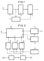
- Figure 1 shows a block diagram of a known ATM cell processing device.
- FIG. 2 shows a diagram of an ATM cell processing device according to the invention.
- FIG. 3 presents an elementary module for FIFO memory of a processing device as shown diagrammatically in FIG. 2.
- FIGS. 4A to 4D and 5A to 5E respectively present timing diagrams for writing and reading the FIFO memory of FIG. 2.
- the known ATM cell processing device presented in FIG. 1, is intended to be included in a broadband communications network equipment exploiting the asynchronous temporal technique called ATM, defined inter alia in an article by Mrs COUDREUSE, PAYS and TROUVAT , entitled “La technique temporelle asynchrone” which appeared in issue 3 of 1990 of the review "Commutation et Transmission” published in Paris, France by SOTELEC.
- This processing device comprises an alignment memory 1, of FIFO type, successively receiving the incoming cells received for example as a series of bytes and fulfilling the functions of rate adaptation and / or plesiosynchronism resolution for these incoming cells. , as previously indicated.
- the output of the alignment memory is connected in parallel to a context processing arrangement 2 and to a delay memory 3.
- the context processing arrangement 2 is capable of taking into account at least some of the bytes which appear at the beginning of the cell, in particular in the field appearing at the head of each cell successively transmitted by the alignment memory 1, it classically deduces therefrom, by using a random access memory not shown, the orientation to be given to the cell whose header field has just been received.
- the delay memory 3 is usually also of the FIFO type, it has the function of delaying the transmission of a cell of the alignment memory 1 to a routing circuit 4 until the moment when this circuit 4 has received the referral indication he expects from the processing arrangement 2 for the cell while awaiting referral.
- the routing circuit 4 then ensures the transmission of the cell as indicated, possibly after having processed it for this transmission.
- the processing device presented in FIG. 2 is intended to transmit cells structured in the same way as those envisaged with the known device presented in FIG. 1, that is to say each with a header field and a field for the information useful to transmit which are of determined formats, these formats being respectively five and forty eight bytes in the case of standardized ATM cells, here taken into account.
- the start of each cell contains, at least at the header field, routing and / or destination indications relating to the cell which contains it.
- a memory 10, of FIFO type, having a particular structure is used to simultaneously ensure the necessary alignment and delay, which makes it possible to eliminate the delay memory provided in the previous embodiments.
- the memory 10 receives the successive cells by a port D with "N" parallel inputs, in the embodiment envisaged here for a processing device intended to operate with ATM cells, this port has thirty-two inputs in the measurement where it is planned to group by words of thirty-two bits fifty two of the fifty three bytes that each cell comprises; the byte not taken into account of each cell is the byte of rank five of the header field, it is indeed a control byte that the equipment receives and processes before reintroducing and transmitting it , without transmitting it via memory 10.
- the memory 10 makes it possible to simultaneously store several cells, for example four, that is to say a number "P" of bits equal to the product of the number "M” of words belonging to the cells in memory by the number "N” of bits of a word.
- the memory 10 comprises two ports A and B parallel with multiple outputs, here thirty-two outputs per port. These two ports A and B are respectively connected one to a routing circuit 14 and the other to a context processing arrangement 12, which are functionally analogous to the routing circuit 4 and to the processing processing context 2 mentioned in connection with Figure 1.
- the memory 10 is commanded in writing by a first generator of pointers 15 which punctuates the successive writes of the words obtained from the successive cells, each from four successive cell bytes, this first generator being controlled by a time base 16 controlled by the external clock signal CKE associated with ATM cells entering memory 10.
- the output of the words at the two ports A and B is here triggered by two pointer generators 17 and 18 each connected to one of the read control ports L1, L2 of the memory and each assigned respectively to one of these output ports.
- These two generators 17 and 18 are controlled by a time base 16 'controlled by a second clock signal CKI, here locally produced; they are associated by means of synchronization devices, not shown, with a memory manager 19, as well as the pointer generator 15.
- the memory manager 19 is likely to be of the usual type acting in a manner known per se, for different states of the memory 10, in particular when this memory 10 is either practically empty or practically full.
- the memory 10 is made up of elementary storage modules O which each make it possible to store two of the "P" binary elements that this memory can store.
- Each elementary memory module O comprises for example two locks 20H and 20L, shown in FIG. 3, having the same data input D and write command inputs E distinct and respectively referenced WH for the lock 20H and WL for the lock 20L .
- an output Q of each lock 20H or 20L attacks a pair of doors 21 and 22, of the three-state type, controlled by separate RA and RB selection signals, such as the pair of doors 21H and 22H connected to the output.
- Two logic circuits 23A and 23B are associated with the assembly formed by the locks 20H, 20L and the doors 21H, 21L, 22H and 22L in the same elementary module 0 to allow transmission to one or the other of the outputs A and B of this module, the bits stored in one or other of the locks 20H, 20L, according to selection signals SA and SB.
- the signals SA and RA, on the one hand, and the signals SB and RB, on the other hand, are produced respectively by the pointer generator 17 and the others by the pointer generator 18 that the base time 16 'regits.
- the logic circuit 23A which comprises the output A of the module is capable of being separately attacked by the two doors 21H and 21L, while the logic circuit 23B which comprises the output B of the module is capable of be attacked separately by the two doors 22H and 22L.
- This offset can be programmed on demand, for example as a function of the cell transfer time so as to change as a function of the operating speed.
- the implementation of a programmable time base 16 ′ allows for example such an evolution of the offset.
- a shift in advance of the signals RB, SB is chosen by twenty-eight byte times "t" with respect to the signals RA, SA, this shift being represented on the timing diagram 5A by the binary value portions one of the synchronization signal SYC whose period "T" is equal to fifty three "t".
- the rising edges of the signal SYC are used to generate a pulse synchronization signal SRA - timing diagram 5B - of period "T" rhythmic the successive appearances of the cells at the output A of memory 10.
- This synchronization signal SRA triggers the addressing successive reading of the memory modules O addressed by the selection signals RA, SA, so that the thirteen words of a cell appear successively at each output A, the four cells simultaneously present in memory 10 at one any given instant successively appearing during four successive "T" periods at output A, in the order in which they were received.
- the timing diagram 5C thus symbolizes the successive appearance of four cells 11, 21, 31, 41 at the output A of the memory 10, each comprising thirteen words of thirty two bits, only the words of rank 0, 1, 11 and 12 of each cell being shown here.
- the falling edges of the signal SYC - timing diagram 5D - are used to generate an impulse signal of synchronization SRB of period "T" punctuating the successive appearances of the cells at the level of the output B of the memory 10, only the words which are intended to be taken into account by the context processing arrangement 12 for one of the cells then stored, for example the words of rank 0 and 1 of the cells in the embodiment envisaged.
- the start of reading can be programmed after the start of writing the second word of a cell, since reading will never catch up with writing.
- the start of the reading of a cell should for example only be programmed after the end of the writing of this cell.
Landscapes
- Engineering & Computer Science (AREA)
- Computer Networks & Wireless Communication (AREA)
- Signal Processing (AREA)
- Data Exchanges In Wide-Area Networks (AREA)
- Communication Control (AREA)
Applications Claiming Priority (2)
| Application Number | Priority Date | Filing Date | Title |
|---|---|---|---|
| FR9214234 | 1992-11-26 | ||
| FR9214234A FR2698463B1 (fr) | 1992-11-26 | 1992-11-26 | Dispositif de traitement de cellules pour équipement de réseau temporel asynchrone de communication. |
Publications (2)
| Publication Number | Publication Date |
|---|---|
| EP0599735A1 true EP0599735A1 (de) | 1994-06-01 |
| EP0599735B1 EP0599735B1 (de) | 2001-04-04 |
Family
ID=9435937
Family Applications (1)
| Application Number | Title | Priority Date | Filing Date |
|---|---|---|---|
| EP93402858A Expired - Lifetime EP0599735B1 (de) | 1992-11-26 | 1993-11-25 | Zellbehandlungsvorrichtung für ein Zeit-Asynchrones Übertragungsnetz |
Country Status (5)
| Country | Link |
|---|---|
| EP (1) | EP0599735B1 (de) |
| AT (1) | ATE200370T1 (de) |
| DE (1) | DE69330083T2 (de) |
| ES (1) | ES2155829T3 (de) |
| FR (1) | FR2698463B1 (de) |
Cited By (1)
| Publication number | Priority date | Publication date | Assignee | Title |
|---|---|---|---|---|
| GB2328590A (en) * | 1997-08-19 | 1999-02-24 | Power X Limited | Data switch |
Citations (2)
| Publication number | Priority date | Publication date | Assignee | Title |
|---|---|---|---|---|
| EP0338558A2 (de) * | 1988-04-21 | 1989-10-25 | Nec Corporation | Für integrierte Schaltungsausführung geeignete Paketvermittlung |
| EP0468498A2 (de) * | 1990-07-26 | 1992-01-29 | Nec Corporation | Leitweglenkungssystem mit Eignung zur effektiven Verarbeitung der Leitweglenkungsinformation |
-
1992
- 1992-11-26 FR FR9214234A patent/FR2698463B1/fr not_active Expired - Fee Related
-
1993
- 1993-11-25 EP EP93402858A patent/EP0599735B1/de not_active Expired - Lifetime
- 1993-11-25 AT AT93402858T patent/ATE200370T1/de not_active IP Right Cessation
- 1993-11-25 DE DE69330083T patent/DE69330083T2/de not_active Expired - Fee Related
- 1993-11-25 ES ES93402858T patent/ES2155829T3/es not_active Expired - Lifetime
Patent Citations (2)
| Publication number | Priority date | Publication date | Assignee | Title |
|---|---|---|---|---|
| EP0338558A2 (de) * | 1988-04-21 | 1989-10-25 | Nec Corporation | Für integrierte Schaltungsausführung geeignete Paketvermittlung |
| EP0468498A2 (de) * | 1990-07-26 | 1992-01-29 | Nec Corporation | Leitweglenkungssystem mit Eignung zur effektiven Verarbeitung der Leitweglenkungsinformation |
Cited By (2)
| Publication number | Priority date | Publication date | Assignee | Title |
|---|---|---|---|---|
| GB2328590A (en) * | 1997-08-19 | 1999-02-24 | Power X Limited | Data switch |
| GB2328590B (en) * | 1997-08-19 | 2002-05-15 | Power X Ltd | Data switching apparatus |
Also Published As
| Publication number | Publication date |
|---|---|
| DE69330083T2 (de) | 2001-11-15 |
| ATE200370T1 (de) | 2001-04-15 |
| ES2155829T3 (es) | 2001-06-01 |
| EP0599735B1 (de) | 2001-04-04 |
| FR2698463B1 (fr) | 1995-01-20 |
| FR2698463A1 (fr) | 1994-05-27 |
| DE69330083D1 (de) | 2001-05-10 |
Similar Documents
| Publication | Publication Date | Title |
|---|---|---|
| EP0293315B1 (de) | System und Verfahren zur Paketflusssteuerung | |
| EP0113307B1 (de) | Anpassungseinrichtung für digitale Informationsblöcke fester Länge | |
| EP0051019B1 (de) | Zählvorrichtung für Hochfrequenzimpulse | |
| EP0138717B1 (de) | Asynchrones digitales Zeitmultiplexsystem mit verteiltem Bus | |
| JPH04220829A (ja) | セル位相乗換回路 | |
| EP0340841B1 (de) | Koppelpunktschaltungselement zwischen zwei Daten-Sammelleitungen | |
| EP0037299B1 (de) | Synchronisierungsanordnung für blockweise übertragene digitale Nachrichten | |
| EP0317863B1 (de) | Verzögerungsvorrichtung für zumindest einen digitalen Hochgeschwindigkeitsdatenstrom | |
| EP0599735B1 (de) | Zellbehandlungsvorrichtung für ein Zeit-Asynchrones Übertragungsnetz | |
| FR2463553A1 (fr) | Procede et circuit d'alignement de donnees pour central telephonique | |
| EP0242915B1 (de) | Einrichtung zur Taktwiedergewinnung für ein Nachrichtenübertragungssystem, welche in einer Übertragungsrichtung mit dem Vielfachzugriff im Zeitmultiplexprinzip arbeitet | |
| EP0249930A1 (de) | Verfahren zur Synchronisation von zwei binären Strömen | |
| EP0064923B1 (de) | System zur Phasensynchronisation digitaler Datenströme und seine Verwendung bei der Umschaltung der Datenströme | |
| EP0406077A1 (de) | Komplementäres verbindungsloses Kommunikationssystem für ein asynchrones Netzwerk | |
| EP0337876B1 (de) | Anordnung zum Vermindern des Energieverbrauchs einer zyklisch arbeitenden Anlage, wie eine Zeitmultiplex-Anlage | |
| EP0435130A1 (de) | Anordnung zum Einfügen binärer Informationselemente in eine bestimmte Rahmenstruktur | |
| EP0018618B1 (de) | Vorrichtung zur Synchronisierung eines Multiplexers in einer Zeitmultiplex-Vermittlungsstelle | |
| EP0707260A1 (de) | Asynchrone Speicheranordnung mit seriellem Zugriff und entsprechendes Speicher- und Leseverfahren | |
| EP0301934B1 (de) | Zeit-Multiplex-Vermittlungssystem für Paketen verschiedener Länge | |
| EP0006798A1 (de) | Digitales Kommunikationssystem mit hohem Datenfluss in einem Maschennetzwerk | |
| EP0689319A1 (de) | Wegesucheapparat für ATM-Zellen | |
| FR2710804A1 (fr) | Dispositif numérique de connexion d'une pluralité de stations de travail sur un réseau local en anneau. | |
| EP0270471A1 (de) | Paketvermittlungssystem | |
| EP0180680B1 (de) | Zählschaltung, insbesondere für Inkrementalgeber und geeignet zur Zusammenarbeit mit einem Acht- oder Sechzehn-Bit-Prozessor | |
| EP0476210A2 (de) | Asynchroner Multiplexer |
Legal Events
| Date | Code | Title | Description |
|---|---|---|---|
| PUAI | Public reference made under article 153(3) epc to a published international application that has entered the european phase |
Free format text: ORIGINAL CODE: 0009012 |
|
| AK | Designated contracting states |
Kind code of ref document: A1 Designated state(s): AT BE CH DE ES FR GB IE IT LI NL PT SE |
|
| 17P | Request for examination filed |
Effective date: 19940916 |
|
| GRAG | Despatch of communication of intention to grant |
Free format text: ORIGINAL CODE: EPIDOS AGRA |
|
| 17Q | First examination report despatched |
Effective date: 20000322 |
|
| GRAG | Despatch of communication of intention to grant |
Free format text: ORIGINAL CODE: EPIDOS AGRA |
|
| GRAH | Despatch of communication of intention to grant a patent |
Free format text: ORIGINAL CODE: EPIDOS IGRA |
|
| GRAH | Despatch of communication of intention to grant a patent |
Free format text: ORIGINAL CODE: EPIDOS IGRA |
|
| RAP1 | Party data changed (applicant data changed or rights of an application transferred) |
Owner name: ALCATEL |
|
| GRAA | (expected) grant |
Free format text: ORIGINAL CODE: 0009210 |
|
| AK | Designated contracting states |
Kind code of ref document: B1 Designated state(s): AT BE CH DE ES FR GB IE IT LI NL PT SE |
|
| PG25 | Lapsed in a contracting state [announced via postgrant information from national office to epo] |
Ref country code: NL Free format text: LAPSE BECAUSE OF FAILURE TO SUBMIT A TRANSLATION OF THE DESCRIPTION OR TO PAY THE FEE WITHIN THE PRESCRIBED TIME-LIMIT Effective date: 20010404 Ref country code: IE Free format text: LAPSE BECAUSE OF FAILURE TO SUBMIT A TRANSLATION OF THE DESCRIPTION OR TO PAY THE FEE WITHIN THE PRESCRIBED TIME-LIMIT Effective date: 20010404 Ref country code: AT Free format text: LAPSE BECAUSE OF FAILURE TO SUBMIT A TRANSLATION OF THE DESCRIPTION OR TO PAY THE FEE WITHIN THE PRESCRIBED TIME-LIMIT Effective date: 20010404 |
|
| REF | Corresponds to: |
Ref document number: 200370 Country of ref document: AT Date of ref document: 20010415 Kind code of ref document: T |
|
| REG | Reference to a national code |
Ref country code: CH Ref legal event code: EP |
|
| GBT | Gb: translation of ep patent filed (gb section 77(6)(a)/1977) |
Effective date: 20010404 |
|
| REG | Reference to a national code |
Ref country code: IE Ref legal event code: FG4D Free format text: FRENCH |
|
| REF | Corresponds to: |
Ref document number: 69330083 Country of ref document: DE Date of ref document: 20010510 |
|
| REG | Reference to a national code |
Ref country code: ES Ref legal event code: FG2A Ref document number: 2155829 Country of ref document: ES Kind code of ref document: T3 |
|
| ITF | It: translation for a ep patent filed | ||
| PG25 | Lapsed in a contracting state [announced via postgrant information from national office to epo] |
Ref country code: PT Free format text: LAPSE BECAUSE OF FAILURE TO SUBMIT A TRANSLATION OF THE DESCRIPTION OR TO PAY THE FEE WITHIN THE PRESCRIBED TIME-LIMIT Effective date: 20010704 |
|
| NLV1 | Nl: lapsed or annulled due to failure to fulfill the requirements of art. 29p and 29m of the patents act | ||
| PGFP | Annual fee paid to national office [announced via postgrant information from national office to epo] |
Ref country code: GB Payment date: 20011012 Year of fee payment: 9 |
|
| PGFP | Annual fee paid to national office [announced via postgrant information from national office to epo] |
Ref country code: DE Payment date: 20011031 Year of fee payment: 9 |
|
| PGFP | Annual fee paid to national office [announced via postgrant information from national office to epo] |
Ref country code: SE Payment date: 20011105 Year of fee payment: 9 |
|
| PGFP | Annual fee paid to national office [announced via postgrant information from national office to epo] |
Ref country code: FR Payment date: 20011106 Year of fee payment: 9 |
|
| PGFP | Annual fee paid to national office [announced via postgrant information from national office to epo] |
Ref country code: ES Payment date: 20011119 Year of fee payment: 9 |
|
| PG25 | Lapsed in a contracting state [announced via postgrant information from national office to epo] |
Ref country code: LI Free format text: LAPSE BECAUSE OF NON-PAYMENT OF DUE FEES Effective date: 20011130 Ref country code: CH Free format text: LAPSE BECAUSE OF NON-PAYMENT OF DUE FEES Effective date: 20011130 Ref country code: BE Free format text: LAPSE BECAUSE OF NON-PAYMENT OF DUE FEES Effective date: 20011130 |
|
| REG | Reference to a national code |
Ref country code: GB Ref legal event code: IF02 |
|
| PLBE | No opposition filed within time limit |
Free format text: ORIGINAL CODE: 0009261 |
|
| STAA | Information on the status of an ep patent application or granted ep patent |
Free format text: STATUS: NO OPPOSITION FILED WITHIN TIME LIMIT |
|
| REG | Reference to a national code |
Ref country code: IE Ref legal event code: FD4D |
|
| 26N | No opposition filed | ||
| BERE | Be: lapsed |
Owner name: ALCATEL Effective date: 20011130 |
|
| REG | Reference to a national code |
Ref country code: CH Ref legal event code: PL |
|
| PG25 | Lapsed in a contracting state [announced via postgrant information from national office to epo] |
Ref country code: GB Free format text: LAPSE BECAUSE OF NON-PAYMENT OF DUE FEES Effective date: 20021125 |
|
| PG25 | Lapsed in a contracting state [announced via postgrant information from national office to epo] |
Ref country code: SE Free format text: LAPSE BECAUSE OF NON-PAYMENT OF DUE FEES Effective date: 20021126 Ref country code: ES Free format text: LAPSE BECAUSE OF NON-PAYMENT OF DUE FEES Effective date: 20021126 |
|
| PG25 | Lapsed in a contracting state [announced via postgrant information from national office to epo] |
Ref country code: DE Free format text: LAPSE BECAUSE OF NON-PAYMENT OF DUE FEES Effective date: 20030603 |
|
| EUG | Se: european patent has lapsed | ||
| GBPC | Gb: european patent ceased through non-payment of renewal fee | ||
| PG25 | Lapsed in a contracting state [announced via postgrant information from national office to epo] |
Ref country code: FR Free format text: LAPSE BECAUSE OF NON-PAYMENT OF DUE FEES Effective date: 20030731 |
|
| REG | Reference to a national code |
Ref country code: FR Ref legal event code: ST |
|
| REG | Reference to a national code |
Ref country code: ES Ref legal event code: FD2A Effective date: 20031213 |
|
| PG25 | Lapsed in a contracting state [announced via postgrant information from national office to epo] |
Ref country code: IT Free format text: LAPSE BECAUSE OF NON-PAYMENT OF DUE FEES;WARNING: LAPSES OF ITALIAN PATENTS WITH EFFECTIVE DATE BEFORE 2007 MAY HAVE OCCURRED AT ANY TIME BEFORE 2007. THE CORRECT EFFECTIVE DATE MAY BE DIFFERENT FROM THE ONE RECORDED. Effective date: 20051125 |