EP0406077A1 - Komplementäres verbindungsloses Kommunikationssystem für ein asynchrones Netzwerk - Google Patents
Komplementäres verbindungsloses Kommunikationssystem für ein asynchrones Netzwerk Download PDFInfo
- Publication number
- EP0406077A1 EP0406077A1 EP90401783A EP90401783A EP0406077A1 EP 0406077 A1 EP0406077 A1 EP 0406077A1 EP 90401783 A EP90401783 A EP 90401783A EP 90401783 A EP90401783 A EP 90401783A EP 0406077 A1 EP0406077 A1 EP 0406077A1
- Authority
- EP
- European Patent Office
- Prior art keywords
- terminals
- data cells
- ring
- cells
- virtual ring
- Prior art date
- Legal status (The legal status is an assumption and is not a legal conclusion. Google has not performed a legal analysis and makes no representation as to the accuracy of the status listed.)
- Granted
Links
- 238000004891 communication Methods 0.000 title claims abstract description 21
- 230000000295 complement effect Effects 0.000 title description 3
- 230000005540 biological transmission Effects 0.000 claims abstract description 31
- 238000004519 manufacturing process Methods 0.000 claims abstract description 3
- 230000001276 controlling effect Effects 0.000 claims description 3
- 230000001105 regulatory effect Effects 0.000 claims description 3
- 239000007787 solid Substances 0.000 claims description 2
- 238000005259 measurement Methods 0.000 claims 1
- 230000011664 signaling Effects 0.000 description 5
- 230000006978 adaptation Effects 0.000 description 4
- 238000003780 insertion Methods 0.000 description 4
- 230000037431 insertion Effects 0.000 description 4
- 230000002457 bidirectional effect Effects 0.000 description 3
- 238000010586 diagram Methods 0.000 description 3
- 238000012545 processing Methods 0.000 description 3
- 238000000034 method Methods 0.000 description 2
- 230000003213 activating effect Effects 0.000 description 1
- 238000012986 modification Methods 0.000 description 1
- 230000004048 modification Effects 0.000 description 1
- 230000004044 response Effects 0.000 description 1
- 230000000630 rising effect Effects 0.000 description 1
- 230000002123 temporal effect Effects 0.000 description 1
- 238000012546 transfer Methods 0.000 description 1
- 230000007704 transition Effects 0.000 description 1
- 230000032258 transport Effects 0.000 description 1
Images


Classifications
-
- H—ELECTRICITY
- H04—ELECTRIC COMMUNICATION TECHNIQUE
- H04L—TRANSMISSION OF DIGITAL INFORMATION, e.g. TELEGRAPHIC COMMUNICATION
- H04L12/00—Data switching networks
- H04L12/54—Store-and-forward switching systems
- H04L12/56—Packet switching systems
Definitions
- the present invention is in the field of asynchronous time switching. More specifically, the invention relates to communication systems associated with asynchronous time networks and authorizing communications in connectionless mode between the terminals.
- Asynchronous time networks are designed to provide connection-mode communications, that is, a resource reservation link must necessarily be established between the terminals before each transmission of information.
- the local business networks (LAN - Local Area Network in English terminology) provide services of the connectionless type and a terminal can transmit information at any time to another terminal by specifying only the address of the destination terminal and without the need to establish a connection beforehand.
- a connectionless service is essential for data transmission applications for which a priori are not known: - with which other terminals the requesting terminal will then exchange information; - what volume of information will be transmitted by said requesting terminal, for how long and at what speed; and - the times at which the requesting terminal will transmit.
- the asynchronous temporal technique is generally considered to be a very good technical switching solution due to its speed, and its use is envisaged for the constitution of future digital networks with integrated broadband services (ISDN-LB). Given the qualities and advantages of this technique, it is desirable that it can meet different communication needs.
- a time network asynchronous must be able to respond to requests for connectionless services if only to be usable also in the private domain of local business networks.
- the present invention aims to provide complementary communication systems designed to equip asynchronous time networks and provide them with functionalities of the connectionless type.
- the means distributed in the terminals comprise in each of said terminals demultiplexing and multiplexing means for separating the first data cells of the virtual ring and second data cells not belonging to the virtual ring and conveyed by of the same asynchronous time network multiplexes, means for detecting and receiving the first data cells intended for the terminal, means for reading and memorizing in chronological order of arrival of the information blocks and source addresses read in the first cells of received data, means for retransmitting in the virtual ring the first full data cells intended for other terminals, and means for including blocks of information to be transmitted and addresses in first empty data cells in order to transmitting first cells with said blocks and addresses in the virtual ring.
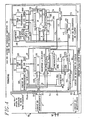
- a communication system in connectionless mode and in a virtual ring is installed in an asynchronous time network RA.
- a plurality of TE terminals are connected to switching nodes N.
- Two-way asynchronous time multiplexes MN connect the nodes N to one another and form a network of any structure.
- Other bidirectional asynchronous time multiplexes MT connect the terminals TE to the nodes N.
- four terminals TE1 to TE4 are connected through the virtual ring.
- Data transmission in the virtual ring is unidirectional.
- the routing of data through the virtual ring is shown in Fig. 1 by arrows in broken lines.
- Ring management equipment GA is provided in the network RA in order to administer the virtual ring.
- the GA equipment is connected to a network node and is integrated into said network.
- the equipment GA is external to the network RA proper and is in the form of a terminal TE dedicated to the function of administration of the virtual ring.
- a multiplex MT connecting a terminal TE n of the virtual ring transports, according to each direction of transmission, data cells CA of length fixed at a predetermined rate.
- the CA data cells belong to the virtual ring and relate to the connectionless connections.
- a CA cell is composed of an AND label and a BI information block.
- the AND label includes a routing word MA, a discrimination word MD, and two signaling bits LIB and FOL.
- the routing word MA allows the routing of cells through the RA network.
- a cell CA received by a terminal TE n of the ring and including a routing word MA n is retransmitted by the latter with another routing word MA n + 1 ⁇ MA n to the following terminal TE n + 1 of the virtual ring.
- the ring management equipment GA at each modification of the virtual ring by connection or disconnection of one or more terminals TE n in the ring, orders the loading of new routing tables in the different nodes N of the network RA and communicates to the terminals of the virtual ring the corresponding routing words MA.
- the discrimination word MD contains a source address AS and a destination address AD corresponding respectively to an address of the terminal TE having included data in the block BI of the cell and to an address of the terminal TE recipient of said data.
- an IFO information frame transmitted by a terminal TE n in connectionless mode to another terminal TE m of the ring is of any length and is divided into several groups of data, for example GD1 to GD4, which are included respectively in information blocks BI1 to BI4 respectively of cells CA1 to CA4 transmitted successively by the terminal TE n .
- the LIB bit in state "1" indicates that cell cA is free and can receive a block of information BI.
- the LIB bit in the "0" state indicates that the CA cell is busy and conveys a valid BI information block.
- the FOL bit is set to "1" by the terminal on this TE m having deposited a group of data GD in the cell CA.
- a TE p terminal has a particular role which is to regulate the flow in the virtual ring and to control the cells conveyed in the ring.
- the terminal TE p is hereinafter called "pilot terminal”.
- each of the TE n terminals is equipped with a ring matching circuit 1 which is now described.
- the ring matching circuit 1 comprises a cell reception circuit 10 and a cell transmission circuit 11.
- multiplexes entering and leaving the bidirectional multiplex MT are respectively connected to a demultiplexing circuit 2 and to a multiplexing circuit 3.
- the demultiplexing 2 and multiplexing 3 circuits essentially have the function of separating first and second channels corresponding respectively to the data cells cA belonging to the virtual ring and to other data cells PA not belonging to the virtual ring.
- First outputs and inputs, 20 and 30, respectively of circuits 2 and 3 are connected to a bidirectional link LA conveying cells PA to corresponding processing circuits of the terminal TE n .
- Second outputs and inputs, 21 and 31, of circuits 2 and 3 are respectively connected to the cell 10 and cell transmission 11 circuits.
- the cell reception circuit 10 essentially comprises input shift registers 100 and 101, a synchronization circuit 102, word comparators 103 and 103a, a counter 104, and reception queues 105.
- the CA cells are delivered in serial form by the demultiplexing circuit 2 and are applied to serial data inputs D of the shift registers 100 and 101 and to a corresponding input of the synchronization circuit 102.
- the synchronization circuit 102 receives the cells CA and outputs a bit rate clock signal HB and a start of frame signal DT to signal in state "1" the reception of a first cell CA1 (Fig. 3) conveying a first group of data GD1 (FIG. 3) of an IFO information frame transmitted through the ring.
- the clock signal HB is applied directly to a clock input CL of the shift register 100 and, through an AND gate, 1010, to another CL input of the shift register 101.
- the bits of the cells CA are loaded successively and continuously into the shift register 100.
- the register 100 comprises four fields corresponding respectively to the routing word MA, the signaling bit LIB, the signaling bit FOL, and the word MD discrimination.
- the comparator 103 has the function of detecting the loading in the register 100 of an ET tag in order to signal the reception of a data cell CA.
- the comparator 103 receives at the first inputs a portion of routing word MA * common to all the routing words MA included in the cells CA. Second inputs of comparator 103 are connected to parallel outputs of register 100 corresponding to the field of the word MA.
- a pulse CR "1" is supplied at the output by the comparator 103 when a cell CA is detected.
- the pulse CR is applied to a first input of an AND gate, 1030, and to an input for activating the comparator 103a.
- the comparator 103a detects in the register 100 the discrimination words MD containing a destination address AD identical to an address AD n corresponding to the terminal TE n .
- the pulse CRa is applied to an initialization input RAZ of the counter 104 and to a first input of an AND gate, 1031.
- the counter 104 is a binary modulo N counter, where N is the length in number of bits of the information block BI of a cell CA.
- the content of counter 104 is incremented cyclically by the clock signal HB.
- a signal SI is delivered by the counter 104.
- the signal SI is in the state “0” and in the state "1” respectively when the counter 104 is blocked and when it is released.
- the falling edge, from "1" to "0" , of the signal SI controls in the reception queues 105 the loading of the state of the start of frame signal DT which is supplied by the synchronization circuit 102, of the information block BI which is supplied by corresponding parallel outputs of the register 101, and the source address AS which is contained in the discrimination word MD and supplied by corresponding parallel outputs of the register 100.
- the reception queues 105 are of FIFO type and store the information DT, BI and AS in order chronological arrival of CA cells. The information stored in the reception queues 105 is then transferred to upper processing layers of the terminal TE n .
- a logic inverter 1032 and an OR gate, 1033 are also provided in the cell reception circuit 10 and are associated with AND gates, 1030 and 1031 in order to produce a CLI signal intended for the cell transmission circuit 11.
- the CLI signal to the state "1" indicates to the transmission circuit 11 that a free cell CA is available and ready to receive a block of information BI to be transmitted in the virtual ring.
- the signal CLI is produced in the reception circuit 10 as a function of the signals CR, CRa and LIB and is in the state "1" when a free cell CA is received in the circuit 10 or when a full cell CA intended for the terminal TE n is received and becomes free after the transfer of the information block BI which it contains to the reception queues 105.
- the signal LIB is applied directly to a second input of the AND gate, 1030 and through the inverter 1032, to a second input of the AND gate, 1031.
- Outputs of the AND gates, 1030, and 1031 are connected respectively to first and second inputs of the OR gate, 1033.
- the OR gate, 1033 provides the CLI signal.
- the cell transmission circuit 11 essentially comprises transmission queues 110, output shift registers 111 and 112, a first counter 113, a multiplexer 114, and a second counter 115.
- the information DT, BI and MD transmitted by the upper processing layers of the terminal TE n are stored in the transmission queues 110.
- the register 111 comprises four fields corresponding respectively the routing word MA, the signaling bit FOL, the signaling bit LIB, and the discrimination word MD.
- the register 112 includes a single field intended to receive a block of information BI.
- the two registers 111 and 112 are connected in series.
- a serial Q data output of register 112 is connected to a serial data input D of register 111.
- a bit rate clock signal HB is applied to clock inputs CL of registers 111 and 112.
- the information MD and BI supplied by the transmission queues 110 are applied to corresponding parallel inputs of registers 111 and 11 respectively.
- the routing word MA is applied to corresponding parallel inputs of register 111.
- a parallel entry of register 111 corresponding to the field of the bit FOL is set to state "1".
- Another parallel input of register 111 corresponding to the field of bit LIB is connected to an output of an AND gate, 116, through a logic inverter 1160, and receives a pulse TB.
- the counter 113 is a binary modulo counter M, where M is the length in number of bits of a cell CA.
- the content of the counter 113 is incremented cyclically by the clock signal HB.
- a signal CT is delivered by the counter 113 and is applied to a control input of the multiplexer 114.
- the signal CT is in the state “0” and in the state "1” respectively when the counter 113 is blocked and when it is unlocked.
- the output 21 of the demultiplexing circuit 2 When the CLI pulse is not active and is therefore in the "0" state, the output 21 of the demultiplexing circuit 2 must be looped over the input 31 of the multiplexing circuit 3 so as to retransmit the full cells CA received by the reception circuit 10 to the asynchronous multiplex MT.
- the counter 113 remains blocked and the signal CT in the state "0" selects a first input of the multiplexer 114 connected to a data output Q of the register 100 in the reception circuit 10.
- a output of the multiplexer 114 is connected to the input 31 of the multiplexing circuit 3 and the solid cells CA are transmitted from the output 21 of the circuit 2 to the input 31 of the circuit 3 through the register 100 and the multiplexer 114.
- the CLI pulse is applied to loading command inputs LD of registers 111 and 112 and to a first input of the AND gate, 116.
- Second and third inputs of the AND gate, 116 receive respectively an AT signal and the signal FNV supplied by the transmission queues 110.
- An output of the AND gate, 116 delivers the pulse TB which is applied to a parallel input of the register 111 through the inverter 1160.
- the pulse TB is also applied to an input of control of the transmission queues 110 and control by a state "1" the transmission of the information BI and MD to the corresponding parallel inputs of the registers 111 and 112.
- the AT signal is produced by means in the form of the counter 115 and a NAND gate, 1150 for regulating the transmission rate of the terminal.
- the counter 115 When a maximum value P is reached in the counter 115, the latter is blocked and delivers a signal CB in the state "1".
- the counter 115 is periodically initialized by a low frequency clock signal SD of period T.
- the signal CB is applied to a first input of the NAND gate, 1150.
- a second input of the gate 1150 receives the start signal DT frame from the transmission queues 110.
- the NAND gate, 1150 delivers the AT signal.
- the value P represents a credit in number of information blocks which is allocated to the terminal TE n so that the latter does not monopolize all the debit resources of the virtual ring.
- the signal CS comes to state "1".
- the CB signal is not taken into account and only commands the switching of the AT signal from state "1" to state "0", only when the last information block BI of the packet being transmitted has been transmitted , that is to say when a transition to state "1" of the frame start signal DT is detected.
- a ring pilot circuit 4 which is interposed between the demultiplexing circuit 2 and the ring adaptation circuit 1 included in the pilot terminal TE p .
- a main function of the ring pilot circuit 4 is to regulate the flow rate of the CA cells in the virtual ring by producing and eliminating empty CA cells, according to the cases of figures.
- Another function of the ring pilot circuit 4 is to control the cells CA conveyed in the virtual ring in order to eliminate the cells of full data having accomplished more than a predetermined number of turns in the virtual ring and thus to prevent altered CA cells from rotating indefinitely in the ring.
- the ring driver circuit 4 essentially comprises an input shift register 40, an output shift register 41, a word comparator 42, a buffer register 43, a counter 44, an up-down counter 46, and a cell transmission control circuit 47.
- the cells CA transmitted by the demultiplexing circuit 2 are received at a serial data input D of the input shift register 40.
- a bit rate clock signal HB is applied to a clock input CL of the register d 'entry 40.
- the shift registers 40 and 41 are similar and each comprise M stages so as to allow the loading of a complete CA cell.
- the input register 40 receives the cells CA in serial form and delivers them in parallel form.
- the output register 41 loads the cells CA in parallel form and transmits them in series form to the ring adaptation circuit 1.
- the parallel outputs of the input register 40 corresponding to the fields of the blocks BI and word MD are connected respectively to corresponding parallel inputs of the output register 41.
- the buffer register 43 which is of conventional type, has the function of storing between two receptions of CA cells the bit states FOL and LIB of the last CA cell received.
- the loading of the states of the bits FOL and LIB in the register 43 is controlled by the pulse CRb.
- the counter 44 is a binary modulo M counter.
- the counter 44 operates in a similar manner to the counters 104 and 113 shown in FIG. 4.
- the counter 44 has the function of producing a pulse signal CT1, shown in FIG. 6, having a duration equal to the transmission duration denoted D of a CA cell.
- the signal CT1 produced by the counter 44 is supplied to the cell transmission control circuit 47.
- the up-down counter 46 has the function of determining whether the effective rate DE of the cells in the virtual ring is higher or lower than a predetermined fixed rate DR which is required in the virtual ring.
- the rate clock signal HD has a frequency corresponding to the required rate DR.
- the counter outputs two signals IMF and SUP.
- the signal IMF is in the active state "1" in the case where the effective bit rate DE is less than the required bit rate DR, and then empty cells CA are to be produced.
- the signal SUP is in the active state "1” in the case where the effective bit rate DE is greater than the required bit rate DR, and then empty cells CA are to be deleted.
- the cell transmission control circuit 47 includes several logic gates and a multiplexer 479b.
- the SUP signal is applied to a first input of an AND gate, 470, through an inverter 470a. Second and third inputs of gate 470 respectively receive the signal CT1 and the bit LIB stored in the buffer register 43. An output of gate 470 is connected to a first input of a first OR gate, 471. A second AND gate , 472 receives at first and second inputs the signal INF and a signal CT2, respectively.
- the signal CT2, shown in FIG. 6, is supplied by an output 22 of the demultiplexing circuit 2 and indicates in the state "1" that a free time interval is available for possibly transmitting a free cell CA.
- An output of the gate 472 is connected to a second input of the OR gate, 471.
- a third AND gate, 473 receives through an inverter 474 the LIB bit stored in the buffer register 43. Second and third inputs of gate 473 respectively receive the signal CT1 and the bit FOL stored in the buffer register 43. An output of gate 473 is connected to a third input of OR gate, 471. An output of gate 471 is connected to a first input of a fourth AND gate, 475 of which a second input receives the clock signal HB. An output from the AND gate, 475 is connected to a clock input CL of the output register 41 and delivers a transmission control clock signal HT.
- the FOL and LIB bits provided by the buffer register 43 are also applied respectively to first inputs of a first NAND gate, 476 and of a second OR gate, 477.
- the LIB bit is also applied to a second input of the gate 476 through an inverter 478.
- An output of the gate 476 is connected to a first input of a third OR gate, 479.
- a fourth OR gate 479a receives at a first input the pulse CRb supplied by the comparator 42.
- Second inputs of doors 477, 479 and 479a receive a TCV signal supplied by the AND gate, 472.
- the TCV signal is also applied to a control input of the multiplexer 479b.
- Outputs of the OR gates, 479 and 477 are connected respectively to parallel inputs of the register 41 corresponding to the fields of the bits FOL and LIB.
- An output from the OR gate, 479a commands the output register 41 to load the information applied to the parallel inputs of the register 41.
- First inputs of the multiplexer 479b are connected to parallel outputs of the input register 40 corresponding to the field of the routing word MA.
- Second inputs from multiplexer 479b receive the routing word MAa.
- Outputs of the multiplexer 479b are connected to parallel inputs of the output register 41 corresponding to the field of the routing word MA.
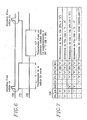
- the signal TCV IMF.CT2 controls in state "1" the transmission of one or more, n ⁇ 1, additional empty CA cells. As is apparent from FIG. 6, the transmission of additional CA empty cells takes place between two receptions of CA cells in the input register 40.
- the notation CAs "0 ...
- 0 means that a state sequence "0" is transmitted in response to the input of the CAe cell and therefore that the CAe cell is eliminated.
- the symbol "-" in the boxes of the table shown in Fig. 7 indicates that the state of the corresponding signal or bit is arbitrary.
Landscapes
- Engineering & Computer Science (AREA)
- Computer Networks & Wireless Communication (AREA)
- Signal Processing (AREA)
- Data Exchanges In Wide-Area Networks (AREA)
- Time-Division Multiplex Systems (AREA)
- Small-Scale Networks (AREA)
Applications Claiming Priority (2)
| Application Number | Priority Date | Filing Date | Title |
|---|---|---|---|
| FR8908762 | 1989-06-30 | ||
| FR8908762A FR2649269B1 (fr) | 1989-06-30 | 1989-06-30 | Systemes complementaires de communication en mode sans-connexion pour reseau temporel asynchrone |
Publications (2)
| Publication Number | Publication Date |
|---|---|
| EP0406077A1 true EP0406077A1 (de) | 1991-01-02 |
| EP0406077B1 EP0406077B1 (de) | 1994-03-30 |
Family
ID=9383309
Family Applications (1)
| Application Number | Title | Priority Date | Filing Date |
|---|---|---|---|
| EP90401783A Expired - Lifetime EP0406077B1 (de) | 1989-06-30 | 1990-06-22 | Komplementäres verbindungsloses Kommunikationssystem für ein asynchrones Netzwerk |
Country Status (7)
| Country | Link |
|---|---|
| US (1) | US5214648A (de) |
| EP (1) | EP0406077B1 (de) |
| JP (1) | JPH03132123A (de) |
| AU (1) | AU629000B2 (de) |
| CA (1) | CA2020132C (de) |
| DE (1) | DE69007694T2 (de) |
| FR (1) | FR2649269B1 (de) |
Families Citing this family (12)
| Publication number | Priority date | Publication date | Assignee | Title |
|---|---|---|---|---|
| CA2049405A1 (en) * | 1990-08-18 | 1992-02-19 | Hiroshi Kobayashi | Broadband switching networks |
| US6411620B1 (en) | 1991-01-31 | 2002-06-25 | Fujitsu Limited | Connectionless communication system |
| CA2104133A1 (en) * | 1992-08-17 | 1994-02-18 | Tsutomu Tanaka | Data transmission system with packets having occupied, idle, released, and reset states |
| USRE39395E1 (en) * | 1992-11-02 | 2006-11-14 | Negotiated Data Solutions Llc | Data communication network with transfer port, cascade port and/or frame synchronizing signal |
| EP0596648A1 (de) | 1992-11-02 | 1994-05-11 | National Semiconductor Corporation | Erkennung du Fähigkeiten eines Netzendpunkts |
| USRE39116E1 (en) | 1992-11-02 | 2006-06-06 | Negotiated Data Solutions Llc | Network link detection and generation |
| EP0596651A1 (de) * | 1992-11-02 | 1994-05-11 | National Semiconductor Corporation | Datennetz mit isochroner Übertragungsfähigkeit |
| US5533018A (en) | 1994-12-21 | 1996-07-02 | National Semiconductor Corporation | Multi-protocol packet framing over an isochronous network |
| US5648969A (en) * | 1995-02-13 | 1997-07-15 | Netro Corporation | Reliable ATM microwave link and network |
| US5936949A (en) * | 1996-09-05 | 1999-08-10 | Netro Corporation | Wireless ATM metropolitan area network |
| JP3537318B2 (ja) | 1998-07-24 | 2004-06-14 | 富士通株式会社 | 特定のコネクションの通信データを加工する交換機および交換方法 |
| US7058027B1 (en) | 1998-09-16 | 2006-06-06 | Scientific Research Corporation | Systems and methods for asynchronous transfer mode and internet protocol |
Citations (2)
| Publication number | Priority date | Publication date | Assignee | Title |
|---|---|---|---|---|
| US4486877A (en) * | 1982-06-25 | 1984-12-04 | At&T Bell Laboratories | Packet switching loop-around network and facilities testing |
| EP0300606A2 (de) * | 1987-07-22 | 1989-01-25 | Gec-Marconi Limited | Ringförmiges lokales Netzwerk |
Family Cites Families (6)
| Publication number | Priority date | Publication date | Assignee | Title |
|---|---|---|---|---|
| JPS61290835A (ja) * | 1985-06-19 | 1986-12-20 | Hitachi Ltd | ル−プ通信方式 |
| US4751697A (en) * | 1986-09-05 | 1988-06-14 | American Telephone And Telegraph Company, At&T Bell Laboratories | Distributed packet switching sytem |
| FR2625858A1 (fr) * | 1988-01-08 | 1989-07-13 | Lmt Radio Professionelle | Procede et dispositif de commutation d'un paquet de donnees |
| CA1294347C (en) * | 1988-05-05 | 1992-01-14 | Man Him Hui | Remote interconnection of local area networks |
| GB8824972D0 (en) * | 1988-10-25 | 1988-11-30 | Plessey Telecomm | Time division switch |
| JP2964151B2 (ja) * | 1989-07-03 | 1999-10-18 | 富士通株式会社 | 通信制御方式 |
-
1989
- 1989-06-30 FR FR8908762A patent/FR2649269B1/fr not_active Expired - Lifetime
-
1990
- 1990-06-22 DE DE69007694T patent/DE69007694T2/de not_active Expired - Fee Related
- 1990-06-22 EP EP90401783A patent/EP0406077B1/de not_active Expired - Lifetime
- 1990-06-25 US US07/542,826 patent/US5214648A/en not_active Expired - Fee Related
- 1990-06-29 CA CA002020132A patent/CA2020132C/en not_active Expired - Fee Related
- 1990-06-29 AU AU58033/90A patent/AU629000B2/en not_active Ceased
- 1990-06-30 JP JP2174351A patent/JPH03132123A/ja active Pending
Patent Citations (2)
| Publication number | Priority date | Publication date | Assignee | Title |
|---|---|---|---|---|
| US4486877A (en) * | 1982-06-25 | 1984-12-04 | At&T Bell Laboratories | Packet switching loop-around network and facilities testing |
| EP0300606A2 (de) * | 1987-07-22 | 1989-01-25 | Gec-Marconi Limited | Ringförmiges lokales Netzwerk |
Non-Patent Citations (3)
| Title |
|---|
| BRITISH TELECOMMUNICATIONS ENGINEERING, vol. 6, no. 2, juillet 1987, pages 95-104, Londres, GB; M. LITTLEWOOD et al.: "Network evolution using asynchronous time-division techniques" * |
| IEE PROCEEDINGS SECTION A a I, vol. 131, no. 2, partie E, mars 1984, pages 38-44, Old Woking, GB; R. HULL et al.: "Virtual resource ring: Technique for decentralised resource management in fault-tolerant distributed computer systems" * |
| INTERNATIONAL SWITCHING SYMPOSIUM 1987, Phoenix, 15-20 mars 1987, pages 462-469, IEEE, Phoenix, Arizona, US; M.Wm. BECKNER et al.: "A protocol and prototype for broadband subscriber access to ISDN's" * |
Also Published As
| Publication number | Publication date |
|---|---|
| EP0406077B1 (de) | 1994-03-30 |
| US5214648A (en) | 1993-05-25 |
| JPH03132123A (ja) | 1991-06-05 |
| DE69007694T2 (de) | 1994-09-15 |
| FR2649269B1 (fr) | 1991-12-20 |
| CA2020132C (en) | 1994-10-18 |
| AU629000B2 (en) | 1992-09-24 |
| FR2649269A1 (fr) | 1991-01-04 |
| DE69007694D1 (de) | 1994-05-05 |
| CA2020132A1 (en) | 1990-12-31 |
| AU5803390A (en) | 1991-01-03 |
Similar Documents
| Publication | Publication Date | Title |
|---|---|---|
| EP0300876B1 (de) | Hybrides Zeit-Multiplex-Vermittlungssystem mit optimal gestaltetem Pufferspeicher | |
| EP0451029B1 (de) | Vermittlungsanordnung zum Durchschalten von Rahmen in einem digitalen und asynchronen Übertragungsnetz | |
| EP0293315B1 (de) | System und Verfahren zur Paketflusssteuerung | |
| EP0406077B1 (de) | Komplementäres verbindungsloses Kommunikationssystem für ein asynchrones Netzwerk | |
| FR2758036A1 (fr) | Commutateur a mode de transfert asynchrone de cellule de plusieurs canaux d'entree a plusieurs canaux de sortie | |
| EP0609137A1 (de) | Umwandlungsvorrichtung zwischen Asynchronen- und Synchronen Übertragungsverfahren | |
| FR2758035A1 (fr) | Commutateur a mode de transfert asynchrone | |
| FR2820921A1 (fr) | Dispositif et procede de transmission dans un commutateur | |
| EP0383660B1 (de) | Ratenreservierung in einem asynchronen Paketnetzwerk | |
| EP0377203B1 (de) | Empfangs- und Bearbeitungssystem für PCM-TDM-mehrwegübertragene HDLC-Rahmen, insbesondere für Datenvermittler | |
| CA2006831C (fr) | Systeme d'emission de trames hdlc sur canal de type mic, a circuit hdlc unique et memoire tampon de transposition | |
| FR2804812A1 (fr) | Procede et dispositif de communication entre un premier et un deuxieme reseau | |
| FR2727818A1 (fr) | Procede d'acheminement de cellules dans un reseau de commutation a multiplexage temporel asynchrone, reseau, commutateur d'entree et application correspondants | |
| EP0340841B1 (de) | Koppelpunktschaltungselement zwischen zwei Daten-Sammelleitungen | |
| FR2549673A1 (fr) | Commutateur elementaire pour autocommutateur utilisant une technique de multiplexage asynchrone | |
| FR2939992A1 (fr) | Procede d'equilibrage de la latence dans un arbre de communication, dispositif, produit programme d'ordinateur et moyen de stockage correspondants | |
| EP0300942A1 (de) | Vermittlungssystem für Datenpakete mit Vorrang | |
| EP0587468A2 (de) | Photonisches Verbindungsnetz mit Rundschreibfähigkeit | |
| EP0337876B1 (de) | Anordnung zum Vermindern des Energieverbrauchs einer zyklisch arbeitenden Anlage, wie eine Zeitmultiplex-Anlage | |
| EP0689371A1 (de) | Kommunikationssystem mit einem Netz und einer Multiplexeinheit | |
| FR2774242A1 (fr) | Systeme et procede de commutation asynchrone de cellules composites, et modules de port d'entree et de port de sortie correspondants | |
| EP0178205B1 (de) | Digitales Netz mit Vielfachzugriff | |
| EP0689319B1 (de) | Wegesucheapparat für ATM-Zellen | |
| EP0301934B1 (de) | Zeit-Multiplex-Vermittlungssystem für Paketen verschiedener Länge | |
| EP0752777B1 (de) | ATM-Koppelfeld |
Legal Events
| Date | Code | Title | Description |
|---|---|---|---|
| PUAI | Public reference made under article 153(3) epc to a published international application that has entered the european phase |
Free format text: ORIGINAL CODE: 0009012 |
|
| AK | Designated contracting states |
Kind code of ref document: A1 Designated state(s): BE DE GB |
|
| 17P | Request for examination filed |
Effective date: 19901130 |
|
| 17Q | First examination report despatched |
Effective date: 19930422 |
|
| RAP1 | Party data changed (applicant data changed or rights of an application transferred) |
Owner name: FRANCE TELECOM |
|
| GRAA | (expected) grant |
Free format text: ORIGINAL CODE: 0009210 |
|
| AK | Designated contracting states |
Kind code of ref document: B1 Designated state(s): BE DE GB |
|
| GBT | Gb: translation of ep patent filed (gb section 77(6)(a)/1977) |
Effective date: 19940329 |
|
| REF | Corresponds to: |
Ref document number: 69007694 Country of ref document: DE Date of ref document: 19940505 |
|
| PG25 | Lapsed in a contracting state [announced via postgrant information from national office to epo] |
Ref country code: BE Effective date: 19940630 |
|
| BERE | Be: lapsed |
Owner name: FRANCE TELECOM Effective date: 19940630 |
|
| PLBE | No opposition filed within time limit |
Free format text: ORIGINAL CODE: 0009261 |
|
| STAA | Information on the status of an ep patent application or granted ep patent |
Free format text: STATUS: NO OPPOSITION FILED WITHIN TIME LIMIT |
|
| 26N | No opposition filed | ||
| REG | Reference to a national code |
Ref country code: GB Ref legal event code: IF02 |
|
| PGFP | Annual fee paid to national office [announced via postgrant information from national office to epo] |
Ref country code: DE Payment date: 20040526 Year of fee payment: 15 |
|
| PGFP | Annual fee paid to national office [announced via postgrant information from national office to epo] |
Ref country code: GB Payment date: 20040602 Year of fee payment: 15 |
|
| PG25 | Lapsed in a contracting state [announced via postgrant information from national office to epo] |
Ref country code: GB Free format text: LAPSE BECAUSE OF NON-PAYMENT OF DUE FEES Effective date: 20050622 |
|
| PG25 | Lapsed in a contracting state [announced via postgrant information from national office to epo] |
Ref country code: DE Free format text: LAPSE BECAUSE OF NON-PAYMENT OF DUE FEES Effective date: 20060103 |
|
| GBPC | Gb: european patent ceased through non-payment of renewal fee |
Effective date: 20050622 |