EP0406077A1 - Complementary connectionless communication system for asynchronous time network - Google Patents
Complementary connectionless communication system for asynchronous time network Download PDFInfo
- Publication number
- EP0406077A1 EP0406077A1 EP90401783A EP90401783A EP0406077A1 EP 0406077 A1 EP0406077 A1 EP 0406077A1 EP 90401783 A EP90401783 A EP 90401783A EP 90401783 A EP90401783 A EP 90401783A EP 0406077 A1 EP0406077 A1 EP 0406077A1
- Authority
- EP
- European Patent Office
- Prior art keywords
- terminals
- data cells
- ring
- cells
- virtual ring
- Prior art date
- Legal status (The legal status is an assumption and is not a legal conclusion. Google has not performed a legal analysis and makes no representation as to the accuracy of the status listed.)
- Granted
Links
- 238000004891 communication Methods 0.000 title claims abstract description 21
- 230000000295 complement effect Effects 0.000 title description 3
- 230000005540 biological transmission Effects 0.000 claims abstract description 31
- 238000004519 manufacturing process Methods 0.000 claims abstract description 3
- 230000001276 controlling effect Effects 0.000 claims description 3
- 230000001105 regulatory effect Effects 0.000 claims description 3
- 239000007787 solid Substances 0.000 claims description 2
- 238000005259 measurement Methods 0.000 claims 1
- 230000011664 signaling Effects 0.000 description 5
- 230000006978 adaptation Effects 0.000 description 4
- 238000003780 insertion Methods 0.000 description 4
- 230000037431 insertion Effects 0.000 description 4
- 230000002457 bidirectional effect Effects 0.000 description 3
- 238000010586 diagram Methods 0.000 description 3
- 238000012545 processing Methods 0.000 description 3
- 238000000034 method Methods 0.000 description 2
- 230000003213 activating effect Effects 0.000 description 1
- 238000012986 modification Methods 0.000 description 1
- 230000004048 modification Effects 0.000 description 1
- 230000004044 response Effects 0.000 description 1
- 230000000630 rising effect Effects 0.000 description 1
- 230000002123 temporal effect Effects 0.000 description 1
- 238000012546 transfer Methods 0.000 description 1
- 230000007704 transition Effects 0.000 description 1
- 230000032258 transport Effects 0.000 description 1
Images


Classifications
-
- H—ELECTRICITY
- H04—ELECTRIC COMMUNICATION TECHNIQUE
- H04L—TRANSMISSION OF DIGITAL INFORMATION, e.g. TELEGRAPHIC COMMUNICATION
- H04L12/00—Data switching networks
- H04L12/54—Store-and-forward switching systems
- H04L12/56—Packet switching systems
Definitions
- the present invention is in the field of asynchronous time switching. More specifically, the invention relates to communication systems associated with asynchronous time networks and authorizing communications in connectionless mode between the terminals.
- Asynchronous time networks are designed to provide connection-mode communications, that is, a resource reservation link must necessarily be established between the terminals before each transmission of information.
- the local business networks (LAN - Local Area Network in English terminology) provide services of the connectionless type and a terminal can transmit information at any time to another terminal by specifying only the address of the destination terminal and without the need to establish a connection beforehand.
- a connectionless service is essential for data transmission applications for which a priori are not known: - with which other terminals the requesting terminal will then exchange information; - what volume of information will be transmitted by said requesting terminal, for how long and at what speed; and - the times at which the requesting terminal will transmit.
- the asynchronous temporal technique is generally considered to be a very good technical switching solution due to its speed, and its use is envisaged for the constitution of future digital networks with integrated broadband services (ISDN-LB). Given the qualities and advantages of this technique, it is desirable that it can meet different communication needs.
- a time network asynchronous must be able to respond to requests for connectionless services if only to be usable also in the private domain of local business networks.
- the present invention aims to provide complementary communication systems designed to equip asynchronous time networks and provide them with functionalities of the connectionless type.
- the means distributed in the terminals comprise in each of said terminals demultiplexing and multiplexing means for separating the first data cells of the virtual ring and second data cells not belonging to the virtual ring and conveyed by of the same asynchronous time network multiplexes, means for detecting and receiving the first data cells intended for the terminal, means for reading and memorizing in chronological order of arrival of the information blocks and source addresses read in the first cells of received data, means for retransmitting in the virtual ring the first full data cells intended for other terminals, and means for including blocks of information to be transmitted and addresses in first empty data cells in order to transmitting first cells with said blocks and addresses in the virtual ring.
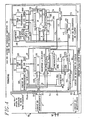
- a communication system in connectionless mode and in a virtual ring is installed in an asynchronous time network RA.
- a plurality of TE terminals are connected to switching nodes N.
- Two-way asynchronous time multiplexes MN connect the nodes N to one another and form a network of any structure.
- Other bidirectional asynchronous time multiplexes MT connect the terminals TE to the nodes N.
- four terminals TE1 to TE4 are connected through the virtual ring.
- Data transmission in the virtual ring is unidirectional.
- the routing of data through the virtual ring is shown in Fig. 1 by arrows in broken lines.
- Ring management equipment GA is provided in the network RA in order to administer the virtual ring.
- the GA equipment is connected to a network node and is integrated into said network.
- the equipment GA is external to the network RA proper and is in the form of a terminal TE dedicated to the function of administration of the virtual ring.
- a multiplex MT connecting a terminal TE n of the virtual ring transports, according to each direction of transmission, data cells CA of length fixed at a predetermined rate.
- the CA data cells belong to the virtual ring and relate to the connectionless connections.
- a CA cell is composed of an AND label and a BI information block.
- the AND label includes a routing word MA, a discrimination word MD, and two signaling bits LIB and FOL.
- the routing word MA allows the routing of cells through the RA network.
- a cell CA received by a terminal TE n of the ring and including a routing word MA n is retransmitted by the latter with another routing word MA n + 1 ⁇ MA n to the following terminal TE n + 1 of the virtual ring.
- the ring management equipment GA at each modification of the virtual ring by connection or disconnection of one or more terminals TE n in the ring, orders the loading of new routing tables in the different nodes N of the network RA and communicates to the terminals of the virtual ring the corresponding routing words MA.
- the discrimination word MD contains a source address AS and a destination address AD corresponding respectively to an address of the terminal TE having included data in the block BI of the cell and to an address of the terminal TE recipient of said data.
- an IFO information frame transmitted by a terminal TE n in connectionless mode to another terminal TE m of the ring is of any length and is divided into several groups of data, for example GD1 to GD4, which are included respectively in information blocks BI1 to BI4 respectively of cells CA1 to CA4 transmitted successively by the terminal TE n .
- the LIB bit in state "1" indicates that cell cA is free and can receive a block of information BI.
- the LIB bit in the "0" state indicates that the CA cell is busy and conveys a valid BI information block.
- the FOL bit is set to "1" by the terminal on this TE m having deposited a group of data GD in the cell CA.
- a TE p terminal has a particular role which is to regulate the flow in the virtual ring and to control the cells conveyed in the ring.
- the terminal TE p is hereinafter called "pilot terminal”.
- each of the TE n terminals is equipped with a ring matching circuit 1 which is now described.
- the ring matching circuit 1 comprises a cell reception circuit 10 and a cell transmission circuit 11.
- multiplexes entering and leaving the bidirectional multiplex MT are respectively connected to a demultiplexing circuit 2 and to a multiplexing circuit 3.
- the demultiplexing 2 and multiplexing 3 circuits essentially have the function of separating first and second channels corresponding respectively to the data cells cA belonging to the virtual ring and to other data cells PA not belonging to the virtual ring.
- First outputs and inputs, 20 and 30, respectively of circuits 2 and 3 are connected to a bidirectional link LA conveying cells PA to corresponding processing circuits of the terminal TE n .
- Second outputs and inputs, 21 and 31, of circuits 2 and 3 are respectively connected to the cell 10 and cell transmission 11 circuits.
- the cell reception circuit 10 essentially comprises input shift registers 100 and 101, a synchronization circuit 102, word comparators 103 and 103a, a counter 104, and reception queues 105.
- the CA cells are delivered in serial form by the demultiplexing circuit 2 and are applied to serial data inputs D of the shift registers 100 and 101 and to a corresponding input of the synchronization circuit 102.
- the synchronization circuit 102 receives the cells CA and outputs a bit rate clock signal HB and a start of frame signal DT to signal in state "1" the reception of a first cell CA1 (Fig. 3) conveying a first group of data GD1 (FIG. 3) of an IFO information frame transmitted through the ring.
- the clock signal HB is applied directly to a clock input CL of the shift register 100 and, through an AND gate, 1010, to another CL input of the shift register 101.
- the bits of the cells CA are loaded successively and continuously into the shift register 100.
- the register 100 comprises four fields corresponding respectively to the routing word MA, the signaling bit LIB, the signaling bit FOL, and the word MD discrimination.
- the comparator 103 has the function of detecting the loading in the register 100 of an ET tag in order to signal the reception of a data cell CA.
- the comparator 103 receives at the first inputs a portion of routing word MA * common to all the routing words MA included in the cells CA. Second inputs of comparator 103 are connected to parallel outputs of register 100 corresponding to the field of the word MA.
- a pulse CR "1" is supplied at the output by the comparator 103 when a cell CA is detected.
- the pulse CR is applied to a first input of an AND gate, 1030, and to an input for activating the comparator 103a.
- the comparator 103a detects in the register 100 the discrimination words MD containing a destination address AD identical to an address AD n corresponding to the terminal TE n .
- the pulse CRa is applied to an initialization input RAZ of the counter 104 and to a first input of an AND gate, 1031.
- the counter 104 is a binary modulo N counter, where N is the length in number of bits of the information block BI of a cell CA.
- the content of counter 104 is incremented cyclically by the clock signal HB.
- a signal SI is delivered by the counter 104.
- the signal SI is in the state “0” and in the state "1” respectively when the counter 104 is blocked and when it is released.
- the falling edge, from "1" to "0" , of the signal SI controls in the reception queues 105 the loading of the state of the start of frame signal DT which is supplied by the synchronization circuit 102, of the information block BI which is supplied by corresponding parallel outputs of the register 101, and the source address AS which is contained in the discrimination word MD and supplied by corresponding parallel outputs of the register 100.
- the reception queues 105 are of FIFO type and store the information DT, BI and AS in order chronological arrival of CA cells. The information stored in the reception queues 105 is then transferred to upper processing layers of the terminal TE n .
- a logic inverter 1032 and an OR gate, 1033 are also provided in the cell reception circuit 10 and are associated with AND gates, 1030 and 1031 in order to produce a CLI signal intended for the cell transmission circuit 11.
- the CLI signal to the state "1" indicates to the transmission circuit 11 that a free cell CA is available and ready to receive a block of information BI to be transmitted in the virtual ring.
- the signal CLI is produced in the reception circuit 10 as a function of the signals CR, CRa and LIB and is in the state "1" when a free cell CA is received in the circuit 10 or when a full cell CA intended for the terminal TE n is received and becomes free after the transfer of the information block BI which it contains to the reception queues 105.
- the signal LIB is applied directly to a second input of the AND gate, 1030 and through the inverter 1032, to a second input of the AND gate, 1031.
- Outputs of the AND gates, 1030, and 1031 are connected respectively to first and second inputs of the OR gate, 1033.
- the OR gate, 1033 provides the CLI signal.
- the cell transmission circuit 11 essentially comprises transmission queues 110, output shift registers 111 and 112, a first counter 113, a multiplexer 114, and a second counter 115.
- the information DT, BI and MD transmitted by the upper processing layers of the terminal TE n are stored in the transmission queues 110.
- the register 111 comprises four fields corresponding respectively the routing word MA, the signaling bit FOL, the signaling bit LIB, and the discrimination word MD.
- the register 112 includes a single field intended to receive a block of information BI.
- the two registers 111 and 112 are connected in series.
- a serial Q data output of register 112 is connected to a serial data input D of register 111.
- a bit rate clock signal HB is applied to clock inputs CL of registers 111 and 112.
- the information MD and BI supplied by the transmission queues 110 are applied to corresponding parallel inputs of registers 111 and 11 respectively.
- the routing word MA is applied to corresponding parallel inputs of register 111.
- a parallel entry of register 111 corresponding to the field of the bit FOL is set to state "1".
- Another parallel input of register 111 corresponding to the field of bit LIB is connected to an output of an AND gate, 116, through a logic inverter 1160, and receives a pulse TB.
- the counter 113 is a binary modulo counter M, where M is the length in number of bits of a cell CA.
- the content of the counter 113 is incremented cyclically by the clock signal HB.
- a signal CT is delivered by the counter 113 and is applied to a control input of the multiplexer 114.
- the signal CT is in the state “0” and in the state "1” respectively when the counter 113 is blocked and when it is unlocked.
- the output 21 of the demultiplexing circuit 2 When the CLI pulse is not active and is therefore in the "0" state, the output 21 of the demultiplexing circuit 2 must be looped over the input 31 of the multiplexing circuit 3 so as to retransmit the full cells CA received by the reception circuit 10 to the asynchronous multiplex MT.
- the counter 113 remains blocked and the signal CT in the state "0" selects a first input of the multiplexer 114 connected to a data output Q of the register 100 in the reception circuit 10.
- a output of the multiplexer 114 is connected to the input 31 of the multiplexing circuit 3 and the solid cells CA are transmitted from the output 21 of the circuit 2 to the input 31 of the circuit 3 through the register 100 and the multiplexer 114.
- the CLI pulse is applied to loading command inputs LD of registers 111 and 112 and to a first input of the AND gate, 116.
- Second and third inputs of the AND gate, 116 receive respectively an AT signal and the signal FNV supplied by the transmission queues 110.
- An output of the AND gate, 116 delivers the pulse TB which is applied to a parallel input of the register 111 through the inverter 1160.
- the pulse TB is also applied to an input of control of the transmission queues 110 and control by a state "1" the transmission of the information BI and MD to the corresponding parallel inputs of the registers 111 and 112.
- the AT signal is produced by means in the form of the counter 115 and a NAND gate, 1150 for regulating the transmission rate of the terminal.
- the counter 115 When a maximum value P is reached in the counter 115, the latter is blocked and delivers a signal CB in the state "1".
- the counter 115 is periodically initialized by a low frequency clock signal SD of period T.
- the signal CB is applied to a first input of the NAND gate, 1150.
- a second input of the gate 1150 receives the start signal DT frame from the transmission queues 110.
- the NAND gate, 1150 delivers the AT signal.
- the value P represents a credit in number of information blocks which is allocated to the terminal TE n so that the latter does not monopolize all the debit resources of the virtual ring.
- the signal CS comes to state "1".
- the CB signal is not taken into account and only commands the switching of the AT signal from state "1" to state "0", only when the last information block BI of the packet being transmitted has been transmitted , that is to say when a transition to state "1" of the frame start signal DT is detected.
- a ring pilot circuit 4 which is interposed between the demultiplexing circuit 2 and the ring adaptation circuit 1 included in the pilot terminal TE p .
- a main function of the ring pilot circuit 4 is to regulate the flow rate of the CA cells in the virtual ring by producing and eliminating empty CA cells, according to the cases of figures.
- Another function of the ring pilot circuit 4 is to control the cells CA conveyed in the virtual ring in order to eliminate the cells of full data having accomplished more than a predetermined number of turns in the virtual ring and thus to prevent altered CA cells from rotating indefinitely in the ring.
- the ring driver circuit 4 essentially comprises an input shift register 40, an output shift register 41, a word comparator 42, a buffer register 43, a counter 44, an up-down counter 46, and a cell transmission control circuit 47.
- the cells CA transmitted by the demultiplexing circuit 2 are received at a serial data input D of the input shift register 40.
- a bit rate clock signal HB is applied to a clock input CL of the register d 'entry 40.
- the shift registers 40 and 41 are similar and each comprise M stages so as to allow the loading of a complete CA cell.
- the input register 40 receives the cells CA in serial form and delivers them in parallel form.
- the output register 41 loads the cells CA in parallel form and transmits them in series form to the ring adaptation circuit 1.
- the parallel outputs of the input register 40 corresponding to the fields of the blocks BI and word MD are connected respectively to corresponding parallel inputs of the output register 41.
- the buffer register 43 which is of conventional type, has the function of storing between two receptions of CA cells the bit states FOL and LIB of the last CA cell received.
- the loading of the states of the bits FOL and LIB in the register 43 is controlled by the pulse CRb.
- the counter 44 is a binary modulo M counter.
- the counter 44 operates in a similar manner to the counters 104 and 113 shown in FIG. 4.
- the counter 44 has the function of producing a pulse signal CT1, shown in FIG. 6, having a duration equal to the transmission duration denoted D of a CA cell.
- the signal CT1 produced by the counter 44 is supplied to the cell transmission control circuit 47.
- the up-down counter 46 has the function of determining whether the effective rate DE of the cells in the virtual ring is higher or lower than a predetermined fixed rate DR which is required in the virtual ring.
- the rate clock signal HD has a frequency corresponding to the required rate DR.
- the counter outputs two signals IMF and SUP.
- the signal IMF is in the active state "1" in the case where the effective bit rate DE is less than the required bit rate DR, and then empty cells CA are to be produced.
- the signal SUP is in the active state "1” in the case where the effective bit rate DE is greater than the required bit rate DR, and then empty cells CA are to be deleted.
- the cell transmission control circuit 47 includes several logic gates and a multiplexer 479b.
- the SUP signal is applied to a first input of an AND gate, 470, through an inverter 470a. Second and third inputs of gate 470 respectively receive the signal CT1 and the bit LIB stored in the buffer register 43. An output of gate 470 is connected to a first input of a first OR gate, 471. A second AND gate , 472 receives at first and second inputs the signal INF and a signal CT2, respectively.
- the signal CT2, shown in FIG. 6, is supplied by an output 22 of the demultiplexing circuit 2 and indicates in the state "1" that a free time interval is available for possibly transmitting a free cell CA.
- An output of the gate 472 is connected to a second input of the OR gate, 471.
- a third AND gate, 473 receives through an inverter 474 the LIB bit stored in the buffer register 43. Second and third inputs of gate 473 respectively receive the signal CT1 and the bit FOL stored in the buffer register 43. An output of gate 473 is connected to a third input of OR gate, 471. An output of gate 471 is connected to a first input of a fourth AND gate, 475 of which a second input receives the clock signal HB. An output from the AND gate, 475 is connected to a clock input CL of the output register 41 and delivers a transmission control clock signal HT.
- the FOL and LIB bits provided by the buffer register 43 are also applied respectively to first inputs of a first NAND gate, 476 and of a second OR gate, 477.
- the LIB bit is also applied to a second input of the gate 476 through an inverter 478.
- An output of the gate 476 is connected to a first input of a third OR gate, 479.
- a fourth OR gate 479a receives at a first input the pulse CRb supplied by the comparator 42.
- Second inputs of doors 477, 479 and 479a receive a TCV signal supplied by the AND gate, 472.
- the TCV signal is also applied to a control input of the multiplexer 479b.
- Outputs of the OR gates, 479 and 477 are connected respectively to parallel inputs of the register 41 corresponding to the fields of the bits FOL and LIB.
- An output from the OR gate, 479a commands the output register 41 to load the information applied to the parallel inputs of the register 41.
- First inputs of the multiplexer 479b are connected to parallel outputs of the input register 40 corresponding to the field of the routing word MA.
- Second inputs from multiplexer 479b receive the routing word MAa.
- Outputs of the multiplexer 479b are connected to parallel inputs of the output register 41 corresponding to the field of the routing word MA.
- the signal TCV IMF.CT2 controls in state "1" the transmission of one or more, n ⁇ 1, additional empty CA cells. As is apparent from FIG. 6, the transmission of additional CA empty cells takes place between two receptions of CA cells in the input register 40.
- the notation CAs "0 ...
- 0 means that a state sequence "0" is transmitted in response to the input of the CAe cell and therefore that the CAe cell is eliminated.
- the symbol "-" in the boxes of the table shown in Fig. 7 indicates that the state of the corresponding signal or bit is arbitrary.
Landscapes
- Engineering & Computer Science (AREA)
- Computer Networks & Wireless Communication (AREA)
- Signal Processing (AREA)
- Data Exchanges In Wide-Area Networks (AREA)
- Time-Division Multiplex Systems (AREA)
- Small-Scale Networks (AREA)
Abstract
Un système de communications selon l'invention est conçu pour équiper un réseau temporel asynchrone (RA) et permettre à des terminaux (TE) raccordés au réseau de communiquer en mode sans-connexion. Le système comprend un équipement de gestion d'anneau (GA) et des moyens répartis dans les terminaux pour interfacer les terminaux à l'anneau virtuel et gérer la production, la réception et la transmission de cellules de données. L'équipement de gestion d'anneau est relié à travers le réseau à chacun des terminaux pour gérer des demandes de connexion/déconnexion émanant des terminaux et pour fournir aux terminaux (TE1 et TE4) connectés à l'anneau des informations relatives à l'acheminement. Un terminal a un rôle particulier de pilote et régule de débit des cellules de données dans l'anneau virtuel. Le terminal-pilote a également pour fonction d'éliminer les cellules altérées. De plus, chacun des terminaux est équipé de moyens pour limiter son débit à une valeur maximale.A communication system according to the invention is designed to equip an asynchronous time network (RA) and allow terminals (TE) connected to the network to communicate in connectionless mode. The system comprises ring management equipment (GA) and means distributed in the terminals for interfacing the terminals to the virtual ring and managing the production, reception and transmission of data cells. The ring management equipment is connected through the network to each of the terminals to manage connection / disconnection requests from the terminals and to provide the terminals (TE1 and TE4) connected to the ring with information relating to the routing. A terminal has a particular role of pilot and regulates the flow of data cells in the virtual ring. The pilot terminal also has the function of eliminating the altered cells. In addition, each of the terminals is equipped with means for limiting its speed to a maximum value.
Description
La présente invention est du domaine de la commutation temporelle asynchrone. Plus précisément, l'invention concerne des systèmes de communication associés à des réseaux temporels asynchrones et autorisant des communications en mode sans-connexion entre les terminaux.The present invention is in the field of asynchronous time switching. More specifically, the invention relates to communication systems associated with asynchronous time networks and authorizing communications in connectionless mode between the terminals.
Les réseaux temporels asynchrones sont conçus pour fournir des communications en mode avec-connexion, c'est-à-dire qu'une liaison avec réservation de ressources doit nécessairement être établie entre les terminaux avant chaque transmission d'informations. Les réseaux locaux d'entreprise (LAN - Local Area Network en terminologie anglo-saxonne) fournissent des services de type sans-connexion et un terminal peut émettre à tout moment des informations vers un autre terminal en précisant uniquement l'adresse du terminal destinataire et sans qu'il soit nécessaire d'établir préalablement une liaison. Un service sans-connexion est essentiel pour des applications de transmission de données pour lesquelles a priori ne sont pas connus :
- avec quels autres terminaux le terminal demandeur va ensuite échanger des informations ;
- quel volume d'information va transmettre ledit terminal demandeur, pendant combien de temps et à quel débit ; et
- les moments auxquels le terminal demandeur va transmettre.Asynchronous time networks are designed to provide connection-mode communications, that is, a resource reservation link must necessarily be established between the terminals before each transmission of information. The local business networks (LAN - Local Area Network in English terminology) provide services of the connectionless type and a terminal can transmit information at any time to another terminal by specifying only the address of the destination terminal and without the need to establish a connection beforehand. A connectionless service is essential for data transmission applications for which a priori are not known:
- with which other terminals the requesting terminal will then exchange information;
- what volume of information will be transmitted by said requesting terminal, for how long and at what speed; and
- the times at which the requesting terminal will transmit.
En effet, une telle imprévisibilité au niveau des paramètres d'une communication rend le service avec-connexion peu rentable. Le taux d'occupation de la liaison n'est pas connu et la durée d'établissement de la liaison lorsqu'une requête de transmission intervient risque d'être disproportionnée par rapport à la durée de transmission de l'information.Indeed, such unpredictability in the parameters of a communication makes the over-connection service unprofitable. The link occupancy rate is not known and the duration of establishment of the link when a transmission request occurs risks being disproportionate to the duration of information transmission.
La technique temporelle asynchrone est considérée généralement comme une très bonne solution technique de commutation de par sa rapidité, et son utilisation est envisagée pour la constitution des futurs réseaux numériques à intégration de services à large bande (RNIS-LB). Compte-tenu des qualités et atouts que présente cette technique, il est souhaitable qu'elle puisse répondre aux différents besoins de communication. Un réseau temporel asynchrone doit pouvoir répondre aux demandes de services sans-connexion ne serait-ce que pour être utilisable également dans le domaine privé des réseaux locaux d'entreprise.The asynchronous temporal technique is generally considered to be a very good technical switching solution due to its speed, and its use is envisaged for the constitution of future digital networks with integrated broadband services (ISDN-LB). Given the qualities and advantages of this technique, it is desirable that it can meet different communication needs. A time network asynchronous must be able to respond to requests for connectionless services if only to be usable also in the private domain of local business networks.
La présente invention vise à fournir des systèmes complémentaires de communication conçus pour équiper des réseaux temporels asynchrones et leur apporter des fonctionnalités de type sans-connexion.The present invention aims to provide complementary communication systems designed to equip asynchronous time networks and provide them with functionalities of the connectionless type.
A cette fin, un système de communication selon l'invention pour équiper un réseau temporel asynchrone et permettre à des terminaux de communiquer en mode sans-connexion à travers ledit réseau est caractérisé en ce que le système comprend des moyens pour gérer l'établissement et l'exploitation d'un anneau virtuel de communication auquel sont connectés les terminaux susceptibles de communiquer entre eux en mode sans-connexion et à travers lequel sont transmises des premières cellules de données contenant des blocs d'information à transmettre, lesdits moyens pour gérer incluant des moyens reliés à travers le réseau à chacun des terminaux pour contrôler des demandes de connexion/déconnexion émanant des terminaux afin de fournir aux terminaux connectés à l'anneau des informations relatives à l'acheminement des cellules, et des moyens répartis dans les terminaux et interfaçant les terminaux à l'anneau virtuel pour gérer la production, la réception et la transmission des premières cellules de données.To this end, a communication system according to the invention for equipping an asynchronous time network and allowing terminals to communicate in connectionless mode through said network is characterized in that the system comprises means for managing the establishment and the operation of a virtual communication ring to which the terminals capable of communicating with each other in connectionless mode are connected and through which are transmitted first data cells containing blocks of information to be transmitted, said means for managing including means connected across the network to each of the terminals for controlling connection / disconnection requests emanating from the terminals in order to provide the terminals connected to the ring with information relating to the routing of the cells, and means distributed in the terminals and interfacing the terminals to the virtual ring to manage production, reception and transmission first data cells.
De préférence, les moyens répartis dans les terminaux comprennent dans chacun desdits terminaux des moyens de démultiplexage et multiplexage pour séparer les premières cellules de données de l'anneau virtuel et des secondes cellules de données n'appartenant pas à l'anneau virtuel et convoyées par des mêmes multiplex temporels asynchrones du réseau, des moyens pour détecter et recevoir les premières cellules de données destinées au terminal, des moyens pour lire et mémoriser par ordre chronologique d'arrivée des blocs d'information et des adresses de source lus dans les premières cellules de données reçues, des moyens pour retransmettre dans l'anneau virtuel les premières cellules de données pleines destinées à d'autres terminaux, et des moyens pour inclure des blocs d'information à transmettre et des adresses dans des premières cellules de données vides afin de transmettre des premières cellules avec lesdits blocs et adresses dans l'anneau virtuel.Preferably, the means distributed in the terminals comprise in each of said terminals demultiplexing and multiplexing means for separating the first data cells of the virtual ring and second data cells not belonging to the virtual ring and conveyed by of the same asynchronous time network multiplexes, means for detecting and receiving the first data cells intended for the terminal, means for reading and memorizing in chronological order of arrival of the information blocks and source addresses read in the first cells of received data, means for retransmitting in the virtual ring the first full data cells intended for other terminals, and means for including blocks of information to be transmitted and addresses in first empty data cells in order to transmitting first cells with said blocks and addresses in the virtual ring.
L'invention sera mieux comprise à la lecture de la description suivante de plusieurs réalisations préférées du système de communication selon l'invention en référence aux dessins annexés correspondants dans lesquels
- - la Fig. 1 montre schématiquement l'architecture d'un réseau temporel asynchrone équipé d'un système de communication selon l'invention ;
- - la Fig. 2 montre la structure de cellules de données convoyées dans un anneau virtuel du système de communication selon l'invention ;
- - la Fig. 3 montre le découpage d'une trame d'information à transmettre en plusieurs blocs d'information et l'insertion des différents blocs dans les cellules de l'anneau ;
- - la Fig. 4 est un bloc-diagramme d'un circuit d'adaptation d'anneau inclus dans chacun des terminaux connectés au réseau ;
- - la Fig. 5 est un bloc-diagramme d'un circuit de pilote d'anneau inclus dans l'un des terminaux connectés au réseau ;
- - la Fig. 6 est un chronogramme montrant l'insertion d'une cellule vide dans l'anneau virtuel du système de communication ; et
- - la Fig. 7 est une table de vérité relative au fonctionnement du circuit pilote d'anneau.
- - Fig. 1 schematically shows the architecture of an asynchronous time network equipped with a communication system according to the invention;
- - Fig. 2 shows the structure of data cells conveyed in a virtual ring of the communication system according to the invention;
- - Fig. 3 shows the division of an information frame to be transmitted into several blocks of information and the insertion of the different blocks in the cells of the ring;
- - Fig. 4 is a block diagram of a ring adaptation circuit included in each of the terminals connected to the network;
- - Fig. 5 is a block diagram of a ring pilot circuit included in one of the terminals connected to the network;
- - Fig. 6 is a timing diagram showing the insertion of an empty cell in the virtual ring of the communication system; and
- - Fig. 7 is a truth table relating to the operation of the ring pilot circuit.
En référence à la Fig. 1, un système de communication en mode sans-connexion et en anneau virtuel selon l'invention est implanté dans un réseau temporel asynchrone RA. Une pluralité de terminaux TE sont raccordés à des noeuds de commutation N. Des multiplex temporels asynchrones bidirectionnels MN relient entre eux les noeuds N et forment un réseau de structure quelconque. D'autres multiplex temporels asynchrones bidirectionnels MT relient les terminaux TE aux noeuds N. A l'instant considéré à la Fig. 1, quatre terminaux TE₁ à TE₄ sont reliés à travers l'anneau virtuel. La transmission des données dans l'anneau virtuel est unidirectionnelle. L'acheminement des données à travers l'anneau virtuel est montré à la Fig. 1 par des flèches en traits interrompus. Un équipement de gestion d'anneau GA est prévu dans le réseau RA afin d'administrer l'anneau virtuel. L'équipement GA est connecté à un noeud du réseau et est intégré audit réseau. Selon une variante, l'équipement GA est extérieur au réseau RA à proprement parler et se présente sous la forme d'un terminal TE dédié à la fonction d'administration de l'anneau virtuel.With reference to FIG. 1, a communication system in connectionless mode and in a virtual ring according to the invention is installed in an asynchronous time network RA. A plurality of TE terminals are connected to switching nodes N. Two-way asynchronous time multiplexes MN connect the nodes N to one another and form a network of any structure. Other bidirectional asynchronous time multiplexes MT connect the terminals TE to the nodes N. At the instant considered in FIG. 1, four terminals TE₁ to TE₄ are connected through the virtual ring. Data transmission in the virtual ring is unidirectional. The routing of data through the virtual ring is shown in Fig. 1 by arrows in broken lines. Ring management equipment GA is provided in the network RA in order to administer the virtual ring. The GA equipment is connected to a network node and is integrated into said network. According to a variant, the equipment GA is external to the network RA proper and is in the form of a terminal TE dedicated to the function of administration of the virtual ring.
Outre des cellules de données relatives à des liaisons avec-connexion, un multiplex MT raccordant un terminal TEn de l'anneau virtuel transporte selon chaque sens de transmission des cellules de données CA de longueur fixe à un débit prédéterminé. Les cellules de données CA appartiennent à l'anneau virtuel et sont relatives aux liaisons sans-connexion.In addition to data cells relating to connection-connection, a multiplex MT connecting a terminal TE n of the virtual ring transports, according to each direction of transmission, data cells CA of length fixed at a predetermined rate. The CA data cells belong to the virtual ring and relate to the connectionless connections.
La structure d'une cellule CA est montrée à la Fig. 2. Une cellule CA est composée d'une étiquette ET et d'un bloc d'information BI.The structure of an CA cell is shown in FIG. 2. A CA cell is composed of an AND label and a BI information block.
L'étiquette ET comprend un mot d'acheminement MA, un mot de discrimination MD, et deux bits de signalisation LIB et FOL.The AND label includes a routing word MA, a discrimination word MD, and two signaling bits LIB and FOL.
Le mot d'acheminement MA permet l'acheminement des cellules à travers le réseau RA. De manière générale, une cellule CA reçue par un terminal TEn de l'anneau et incluant un mot d'acheminement MAn est retransmise par celui-ci avec un autre mot d'acheminement MAn+1≠MAn vers le terminal suivant TEn+1 de l'anneau virtuel. L'équipement de gestion d'anneau GA, à chaque modification de l'anneau virtuel par connexion ou déconnexion d'un ou plusieurs terminaux TEn dans l'anneau, commande le chargement de nouvelles tables d'acheminement dans les différents noeuds N du réseau RA et communique aux terminaux de l'anneau virtuel les mots d'acheminement MA correspondants.The routing word MA allows the routing of cells through the RA network. In general, a cell CA received by a terminal TE n of the ring and including a routing word MA n is retransmitted by the latter with another routing word MA n + 1 ≠ MA n to the following terminal TE n + 1 of the virtual ring. The ring management equipment GA, at each modification of the virtual ring by connection or disconnection of one or more terminals TE n in the ring, orders the loading of new routing tables in the different nodes N of the network RA and communicates to the terminals of the virtual ring the corresponding routing words MA.
Le mot de discrimination MD contient une adresse de source AS et une adresse de destination AD correspondant respectivement à une adresse du terminal TE ayant inclus des données dans le bloc BI de la cellule et à une adresse du terminal TE destinataire desdites données.The discrimination word MD contains a source address AS and a destination address AD corresponding respectively to an address of the terminal TE having included data in the block BI of the cell and to an address of the terminal TE recipient of said data.
En référence à la Fig. 3, une trame d'information IFO transmise par un terminal TEn en mode sans-connexion vers un autre terminal TEm de l'anneau est de longueur quelconque et est découpée en plusieurs groupes de données par exemple GD1 à GD4, lesquels sont inclus respectivement dans des blocs d'information BI1 à BI4 respectivement de cellules CA1 à CA4 transmises successivement par le terminal TEn.With reference to FIG. 3, an IFO information frame transmitted by a terminal TE n in connectionless mode to another terminal TE m of the ring is of any length and is divided into several groups of data, for example GD1 to GD4, which are included respectively in information blocks BI1 to BI4 respectively of cells CA1 to CA4 transmitted successively by the terminal TE n .
Le bit LIB à l'état "1" indique que la cellule cA est libre et peut recevoir un bloc d'information BI. Le bit LIB à l'état "0" indique que la cellule CA est occupée et convoie un bloc d'information BI valide.The LIB bit in state "1" indicates that cell cA is free and can receive a block of information BI. The LIB bit in the "0" state indicates that the CA cell is busy and conveys a valid BI information block.
Le bit FOL est mis à l'état "1" par le terminal sur ce TEm ayant déposé un groupe de données GD dans la cellule CA. Un terminal TEp a un rôle particulier qui est de réguler le débit dans l'anneau virtuel et de contrôler les cellules convoyées dans l'anneau. Le terminal TEp est appelé "terminal pilote" par la suite. Le terminal pilote TEp positionne systématiquement à l'état "0" les bits FOL de toutes les cellules pleines cA (LIB="0") qu'il reçoit avant de les retransmettre dans l'anneau virtuel. Lorsque le terminal pilote TE reçoit une cellule pleine CA avec le bit FOL="0", il en déduit que le mot de discrimination MD est erroné puisque ladite cellule CA a effectué un tour de l'anneau et au maximum deux tours et qu'aucun des terminaux TEn n'a reconnu la cellule comme lui étant destinée, et consécutivement le terminal pilote TEp élimine la cellule CA en ne la retransmettant pas dans l'anneau virtuel.The FOL bit is set to "1" by the terminal on this TE m having deposited a group of data GD in the cell CA. A TE p terminal has a particular role which is to regulate the flow in the virtual ring and to control the cells conveyed in the ring. The terminal TE p is hereinafter called "pilot terminal". The pilot terminal TE p systematically positions the FOL bits of all the full cells cA (LIB = "0") which it receives in the "0" state, which it receives before retransmitting them into the virtual ring. When the pilot terminal TE receives a full cell CA with the bit FOL = "0", it deduces therefrom that the discrimination word MD is erroneous since said cell CA has made one turn of the ring and at most two turns and that none of the terminals TE n has recognized the cell as being intended for it, and consequently the pilot terminal TE p eliminates the CA cell by not retransmitting it in the virtual ring.
En référence à la Fig. 4, chacun des terminaux TEn est équipé d'un circuit d'adaptation d'anneau 1 qui est maintenant décrit. Le circuit d'adaptation d'anneau 1 comprend un circuit de réception de cellule 10 et un circuit de transmission de cellule 11.With reference to FIG. 4, each of the TE n terminals is equipped with a ring matching
Dans le terminal TEn, des multiplex entrant et sortant du multiplex bidirectionnel MT sont reliés respectivement à un circuit de démultiplexage 2 et à un circuit de multiplexage 3. Les circuits de démultiplexage 2 et de multiplexage 3 ont essentiellement pour fonction de séparer des première et seconde voies correspondant respectivement aux cellules de données cA appartenant à l'anneau virtuel et à d'autres cellules de données PA n'appartenant pas à l'anneau virtuel. Des premières sortie et entrée, 20 et 30, respectivement des circuits 2 et 3 sont reliées à une liaison bidirectionnelle LA convoyant des cellules PA vers des circuits de traitement correspondants du terminal TEn. Des secondes sortie et entrée, 21 et 31, des circuits 2 et 3 sont reliées respectivement aux circuits de réception de cellule 10 et de transmission de cellule 11.In the terminal TE n , multiplexes entering and leaving the bidirectional multiplex MT are respectively connected to a
Le circuit de réception de cellule 10 comprend essentiellement des registres à décalage d'entrée 100 et 101, un circuit de synchronisation 102, des comparateurs de mots 103 et 103a, un compteur 104, et des files de réception 105.The
Les cellules CA sont délivrées sous forme série par le circuit de démultiplexage 2 et sont appliquées à des entrées de données série D des registres à décalage 100 et 101 et à une entrée correspondante du circuit de synchronisation 102.The CA cells are delivered in serial form by the
Le circuit de synchronisation 102 reçoit les cellules CA et délivre en sortie un signal d'horloge de rythme de bit HB et un signal de début de trame DT pour signaler à l'état "1" la réception d'une première cellule CA1 (Fig. 3) convoyant un premier groupe de données GD1 (Fig. 3) d'une trame d'information IFO transmise à travers l'anneau.The
Le signal d'horloge HB est appliqué directement à une entrée d'horloge CL du registre à décalage 100 et, à travers une porte ET, 1010, à une autre entrée d'horloge CL du registre à décalage 101.The clock signal HB is applied directly to a clock input CL of the
Les bits des cellules CA sont chargés successivement et de manière continue dans le registre à décalage 100. Le registre 100 comprend quatre champs correspondant respectivement au mot d'acheminement MA, au bit de signalisation LIB, au bit de signalisation FOL, et au mot de discrimination MD.The bits of the cells CA are loaded successively and continuously into the
Le comparateur 103 a pour fonction de détecter le chargement dans le registre 100 d'une étiquette ET afin de signaler la réception d'une cellule de données CA. Le comparateur 103 reçoit à des premières entrées une portion de mot d'acheminement MA* commune à tous les mots d'acheminement MA inclus dans les cellules CA. Des secondes entrées du comparateur 103 sont reliées à des sorties parallèles du registre 100 correspondant au champ du mot MA. Une impulsion CR="1" est fournie en sortie par le comparateur 103 lorsqu'une cellule CA est détectée. L'impulsion CR est appliquée à une première entrée d'une porte ET, 1030, et à une entrée d'activation du comparateur 103a.The
Le comparateur 103a est activé par l'impulsion CR="1" fournie par le comparateur 103. Le comparateur 103a détecte dans le registre 100 les mots de discrimination MD contenant une adresse de destination AD identique à une adresse ADn correspondant au terminal TEn. Lorsqu'une adresse AD=ADn est détectée dans le champ du mot MD correspondant du registre 100, une cellule CA destinée au terminal TEn est en cours de réception et le comparateur 103a délivre une impulsion CRa="1". L'impulsion CRa est appliquée à une entrée d'initialisation RAZ du compteur 104 et à une première entrée d'une porte ET, 1031.The
Le compteur 104 est un compteur binaire modulo N, où N est la longueur en nombre de bits du bloc d'information BI d'une cellule CA. Le contenu du compteur 104 est incrémenté cycliquement par le signal d'horloge HB. Le compteur 104 se bloque lorsque son contenu atteint la valeur M et il est débloqué et remis à zéro par l'impulsion CRa="1". Un signal SI est délivré par le compteur 104. Le signal SI est à l'état "0" et à l'état "1" respectivement lorsque le compteur 104 est bloqué et lorsqu'il est débloqué.The
Lorsqu 'une cellule CA destinée au terminal TEn est en cours de réception, l'impulsion CRa="1" débloque le compteur 104 et le signal SI vient à l'état "1". Le signal SI="1" ouvre la porte ET, 1010, et le signal d'horloge HB est appliqué à l'entrée CL du registre 101. Consécutivement, le bloc d'information BI de la cellule CA en cours de réception est chargé bit par bit dans le registre 101. Lorsque le signal SI commute à l'état "0", la totalité du bloc d'information BI de la cellule CA est chargée dans le registre 101. Le front descendant, de "1" à "0", du signal SI commande dans les files de réception 105 le chargement de l'état du signal de début de trame DT qui est fourni par le circuit de synchronisation 102, du bloc d'information BI qui est fourni par des sorties parallèles correspondantes du registre 101, et de l'adresse de source AS qui est contenue dans le mot de discrimination MD et fournie par des sorties parallèles correspondantes du registre 100. Les files de réception 105 sont de type FIFO et mémorisent les informations DT, BI et AS par ordre chronologique d'arrivée des cellules CA. Les informations stockées dans les files de réception 105 sont ensuite transférées vers des couches de traitement supérieures du terminal TEn.When a cell CA intended for the terminal TE n is being received, the pulse CR a = "1" unlocks the
Un inverseur logique 1032 et une porte OU, 1033 sont également prévus dans le circuit de réception de cellule 10 et sont associés aux portes ET, 1030 et 1031 afin de produire un signal CLI destiné au circuit de transmission de cellule 11. Le signal CLI à l'état "1" indique au circuit de transmission 11 qu'une cellule libre CA est disponible et prête à recevoir un bloc d'information BI à transmettre dans l'anneau virtuel. Le signal CLI est produit dans le circuit de réception 10 en fonction des signaux CR, CRa et LIB et est à l'état "1" lorsqu'une cellule libre CA est reçue dans le circuit 10 ou lorsqu'une cellule pleine CA destinée au terminal TEn est reçue et devient libre après le transfert du bloc d'information BI qu'elle contient vers les files de réception 105. Le signal LIB est appliqué directement à une seconde entrée de la porte ET, 1030 et à travers l'inverseur 1032, à une seconde entrée de la porte ET, 1031. Des sorties des portes ET, 1030, et 1031 sont reliées respectivement à des première et seconde entrées de la porte OU, 1033. La porte OU, 1033 fournit le signal CLI.A
Le circuit de transmission de cellule 11 comprend essentiellement des files de transmission 110, des registres à décalage de sortie 111 et 112, un premier compteur 113, un multiplexeur 114, et un second compteur 115.The cell transmission circuit 11 essentially comprises
Les informations DT, BI et MD transmises par les couches de traitement supérieures du terminal TEn sont stockées dans les files de transmission 110. Outre les informations DT, BI et MD, les files 110 délivrent un signal FNV indiquant à l'état "1" que les files 110 ne sont pas vides, et dans l'état complémentaire FMV = "O" que les files 110 sont vides.The information DT, BI and MD transmitted by the upper processing layers of the terminal TE n are stored in the
Le registre 111 comprênd quatre champs correspondant respectivement au mot d'acheminement MA, au bit de signalisation FOL, au bit de signalisation LIB, et au mot de discrimination MD. Le registre 112 comprend un unique champ destiné à recevoir un bloc d'information BI. Les deux registres 111 et 112 sont connectés en série. Une sortie de données série Q du registre 112 est reliée à une entrée de données série D du registre 111. Un signal d'horloge de rythme de bit HB est appliqué à des entrées d'horloge CL des registres 111 et 112. Les informations MD et BI fournies par les files de transmission 110 sont appliquées à des entrées parallèles correspondantes respectivement des registres 111 et 112. Le mot d'acheminement MA est appliqué à des entrées parallèles correspondantes du registre 111. Une entrée parallèle du registre 111 correspondant au champ du bit FOL est placée à l'état "1". Une autre entrée parallèle du registre 111 correspondant au champ du bit LIB est reliée à une sortie d'une porte ET, 116, à travers un inverseur logique 1160, et reçoit une impulsion TB.The
Le compteur 113 est un compteur binaire modulo M, où M est la longueur en nombre de bits d'une cellule CA. Le contenu du compteur 113 est incrémenté cycliquement par le signal d'horloge HB. Le compteur 113 se bloque lorsque son contenu atteint la valeur M et il est débloqué et remis à zéro par l'impulsion CLI="1" transmise par le circuit de réception de cellule 10 lorsqu'une cellule vide CA est disponible. Un signal CT est délivré par le compteur 113 et est appliqué à une entrée de commande du multiplexeur 114. Le signal CT est à l'état "0" et à l'état "1" respectivement lorsque le compteur 113 est bloqué et lorsqu'il est débloqué.The
Lorsque l'impulsion CLI n'est pas active et est donc à l'état "0", la sortie 21 du circuit de démultiplexage 2 doit être bouclée sur l'entrée 31 du circuit de multiplexage 3 de manière à retransmettre les cellules pleines CA reçues par le circuit de réception 10 vers le multiplex asynchrone MT. Dans le cas de figure ci-dessus, le compteur 113 reste bloqué et le signal CT à l'état "0" sélectionne une première entrée du multiplexeur 114 reliée à une sortie de données Q du registre 100 dans le circuit de réception 10. Une sortie du multiplexeur 114 est reliée à l'entrée 31 du circuit de multiplexage 3 et les cellules pleines CA sont transmises de la sortie 21 du circuit 2 vers l'entrée 31 du circuit 3 à travers le registre 100 et le multiplexeur 114.When the CLI pulse is not active and is therefore in the "0" state, the
Lorsque l'impulsion CLI vient à l'état "1", c'est-à-dire lorsqu'une cellule libre CA est disponible, le compteur 113 est débloqué et est remis à zéro et le signal CT commute à l'état "1" pour une durée correspondant à la transmission d'une cellule CA. Le signal CT="1" sélectionne une seconde entrée du multiplexeur 114, entrée qui est connectée à une sortie de données série Q du registre 111. Suivant le cas, une cellule vide CA ou une cellule CA contenant un bloc d'information BI en provenance des files 110 est transmise vers l'entrée 31 du circuit 3 par les registres 111 et 112.When the CLI pulse comes to state "1", that is to say when a free cell CA is available, the
L'impulsion CLI est appliquée à des entrées de commande de chargement LD des registres 111 et 112 et à une première entrée de la porte ET, 116. Des seconde et troisième entrées de la porte ET, 116 reçoivent respectivement un signal AT et le signal FNV fourni par les files de transmission 110. Une sortie de la porte ET, 116 délivre l'impulsion TB qui est appliquée à une entrée parallèle du registre 111 à travers l'inverseur 1160. L'impulsion TB est également appliquée à une entrée de commande des files de transmission 110 et commande par un état "1" la transmission des informations BI et MD vers les entrées parallèles correspondantes des registres 111 et 112.The CLI pulse is applied to loading command inputs LD of
Lorsque la porte ET, 116 est fermée par l'un des signaux AT ou FNV à l'état "0", l'impulsion CLI ne traverse pas la porte ET, 116 et consécutivement l'impulsion TB="1" n'est pas produite. Les informations BI et MD restent donc dans les files 110 et ne sont pas chargées dans les registres 111 et 112 et l'impulsion CLI commande dans le registre 111 le chargement d'un bit FOL="1", d'un bit LIB=![]()
![]()
Lorsque la porte ET, 116 est ouverte, AT.FNV="1", l'impulsion TB="1" commande le chargement du bit LIB=![]()
![]()
Le signal AT est produit par des moyens sous la forme du compteur 115 et d'une porte NON-ET, 1150 pour réguler le débit de transmission du terminal.The AT signal is produced by means in the form of the
Le compteur 115 est un compteur binaire. Le compteur 115 est incrémenté par les impulsions TB="1" qui sont appliquées à son entrée d'horloge.
Lorsqu'une valeur maximale P est atteinte dans le compteur 115, celui-ci se bloque et délivre un signal CB à l'état "1". Le compteur 115 est initialisé périodiquement par un signal d'horloge SD à basse fréquence de période T. Le signal CB est appliqué à une première entrée de la porte NON-ET, 1150. Une seconde entrée de la porte 1150 reçoit le signal de début de trame DT issu des files de transmission 110. En sortie, la porte NON-ET, 1150 délivre le signal AT.When a maximum value P is reached in the
La valeur P représente un crédit en nombre de blocs d'information qui est alloué au terminal TEn de manière à ce que celui-ci ne monopolise pas toutes les ressources en débit de l'anneau virtuel. Lorsque le terminal TEn a épuisé son crédit, le signal CS vient à l'état "1". Le signal CB n'est pris en compte et ne commande la commutation du signal AT de l'état "1" à l'état "0", que lorsque le dernier bloc d'information BI du paquet en cours de transmission a été transmis, c'est-à-dire lorsqu'une transition vers l'état "1" du signal de début de trame DT est détectée.The value P represents a credit in number of information blocks which is allocated to the terminal TE n so that the latter does not monopolize all the debit resources of the virtual ring. When the terminal TE n has used up its credit, the signal CS comes to state "1". The CB signal is not taken into account and only commands the switching of the AT signal from state "1" to state "0", only when the last information block BI of the packet being transmitted has been transmitted , that is to say when a transition to state "1" of the frame start signal DT is detected.
En référence à la Fig. 5, dans le terminal pilote TEp est prévu un circuit de pilote d'anneau 4 qui est intercalé entre le circuit de démultiplexage 2 et le circuit d'adaptation d'anneau 1 inclus dans le terminal pilote TEp.With reference to FIG. 5, in the pilot terminal TE p is provided a
Une fonction principale du circuit de pilote d'anneau 4 est de réguler le débit des cellules CA dans l'anneau virtuel en produisant et en éliminant des cellules vides CA, selon les cas de figures. Une autre fonction du circuit de pilote d'anneau 4 est de contrôler les cellules CA convoyées dans l'anneau virtuel afin d'éliminer les cellules de données pleines ayant accompli plus qu'un nombre prédéterminé de tours dans l'anneau virtuel et ainsi afin d'éviter que des cellules altérées CA ne puissent tourner indéfiniment dans l'anneau.A main function of the
Le circuit de pilote d'anneau 4 comprend essentiellement un registre à décalage d'entrée 40, un registre à décalage de sortie 41, un comparateur de mots 42, un registre tampon 43, un compteur 44, un compteur-décompteur 46, et un circuit de commande de transmission de cellule 47.The
Les cellules CA transmises par le circuit de démultiplexage 2 sont reçues à une entrée de données série D du registre à décalage d'entrée 40. Un signal d'horloge de rythme de bit HB est appliqué à une entrée d'horloge CL du registre d'entrée 40.The cells CA transmitted by the
Les registres à décalage 40 et 41 sont analogues et comprennent chacun M étages de manière à permettre le chargement d'une cellule CA complète. Le registre d'entrée 40 reçoit les cellules CA sous forme série et les délivre sous forme parallèle. Le registre de sortie 41 charge les cellules CA sous forme parallèle et les transmet sous forme série vers le circuit d'adaptation d'anneau 1. Les sorties parallèles du registre d'entrée 40 correspondant aux champs des bloc BI et mot MD sont reliées respectivement à des entrées parallèles correspondantes du registre de sortie 41.The shift registers 40 and 41 are similar and each comprise M stages so as to allow the loading of a complete CA cell. The input register 40 receives the cells CA in serial form and delivers them in parallel form. The output register 41 loads the cells CA in parallel form and transmits them in series form to the
Le comparateur 42 a pour fonction de détecter le chargement d'une cellule CA dans le registre d'entrée 40. Des premières entrées du comparateur, 42 sont reliées à des sorties parallèles du registre d'entrée 40 correspondant au champ du mot d'acheminement MA. Des secondes entrées du comparateur 42 reçoivent la portion de mot d'acheminement MA* commune à tous les mots d'acheminement MA inclus dans les cellules CA de l'anneau virtuel. Le comparateur 42 fournit une impulsion CRb="1" lorsqu'une cellule CA est chargée dans le registre 40.The
Le registre tampon 43 qui est de type classique, a pour fonction de mémoriser entre deux réceptions de cellules CA les états de bits FOL et LIB de la dernière cellule CA reçue. Le chargement des états des bits FOL et LIB dans le registre 43 est commandé par l'impulsion CRb.The
Le compteur 44 est un compteur binaire modulo M. Le compteur 44 fonctionne de manière analogue aux compteurs 104 et 113 montrés à la Fig. 4. Le compteur 44 a pour fonction de produire un signal impulsionnel CT1, montré à la Fig. 6, ayant une durée égale à la durée de transmission notée D d'une cellule CA. Le déblocage et la remise à zéro du compteur 44 sont commandés sur un front montant de l'impulsion CRb="1". Le signal CT1 produit par le compteur 44 est fourni au circuit de commande de transmission de cellule 47.The
Le compteur-décompteur 46 a pour fonction de déterminer si le débit effectif DE des cellules dans l'anneau virtuel est supérieur ou inférieur à un débit prédéterminé fixe DR qui est requis dans l'anneau virtuel. A cette fin, des entrées d'horloge d'incrémentation + et de décrémentation - du compteur-décompteur reçoivent respectivement les impulsions CRb="1" et un signal d'horloge de débit HD. Le signal d'horloge de débit HD a une fréquence correspondante au débit requis DR. Le compteur délivre en sortie deux signaux IMF et SUP. Le signal IMF est à l'état actif "1" dans le cas où le débit effectif DE est inférieur au débit requis DR, et alors des cellules vides CA sont à produire. Le signal SUP est à l'état actif "1" dans le cas où le débit effectif DE est supérieur au débit requis DR, et alors des cellules vides CA sont à supprimer.The up-
Le circuit de commande de transmission de cellule 47 comprend plusieurs portes logiques et un multiplexeur 479b.The cell transmission control circuit 47 includes several logic gates and a
Le signal SUP est appliqué à une première entrée d'une porte ET, 470, à travers un inverseur 470a. Des seconde et troisième entrées de la porte 470 reçoivent respectivement le signal CT1 et le bit LIB mémorisé dans le registre tampon 43. Une sortie de la porte 470 est connectée à une première entrée d'une première porte OU, 471. Une seconde porte ET, 472 reçoit à des première et seconde entrées le signal INF et un signal CT2, respectivement. Le signal CT2, montré à la Fig. 6, est fourni par une sortie 22 du circuit de démultiplexage 2 et indique à l'état "1" qu'un intervalle temporel libre est disponible pour transmettre éventuellement une cellule libre CA. Une sortie de la porte 472 est reliée à une seconde entrée de la porte OU, 471. A une première entrée, une troisième porte ET, 473 reçoit à travers un inverseur 474 le bit LIB mémorisé dans le registre tampon 43. Des seconde et troisième entrées de la porte 473 reçoivent respectivement le signal CT1 et le bit FOL mémorisé dans le registre tampon 43. Une sortie de la porte 473 est reliée à une troisième entrée de la porte OU, 471. Une sortie de la porte 471 est reliée à une première entrée d'une quatrième porte ET, 475 dont une seconde entrée reçoit le signal d'horloge HB. Une sortie de la porte ET, 475 est connectée à une entrée d'horloge CL du registre de sortie 41 et délivre un signal d'horloge de commande de transmission HT.The SUP signal is applied to a first input of an AND gate, 470, through an
Les bits FOL et LIB fournis par le registre tampon 43 sont également appliqués respectivement à des premières entrées d'une première porte NON-ET, 476 et d'une seconde porte OU, 477. Le bit LIB est également appliqué à une seconde entrée de la porte 476 à travers un inverseur 478. Une sortie de la porte 476 est reliée à une première entrée d'une troisième porte OU, 479. Une quatrième porte OU 479a reçoit à une première entrée l'impulsion CRb fournie par le comparateur 42. Des secondes entrées des portes 477, 479 et 479a reçoivent un signal TCV fourni par la porte ET, 472. Le signal TCV est également appliqué à une entrée de commande du multiplexeur 479b. Des sorties des portes OU, 479 et 477 sont reliées respectivement à des entrées parallèles du registre 41 correspondant aux champs des bits FOL et LIB. Une sortie de la porte OU, 479a commande dans le registre de sortie 41 le chargement des informations appliquées aux entrées parallèles du registre 41.The FOL and LIB bits provided by the
Le multiplexeur 479b a pour fonction de fournir un mot d'acheminement MAa à charger dans le champ correspondant du registre de sortie 41 lorsqu'une cellule vide CA supplémentaire (INF="1") doit être produite et transmise et que le contenu du champ du mot d"acheminement MA dans le registre d'entrée 40 n'est pas valide. Des premières entrées du multiplexeur 479b sont reliées à des sorties parallèles du registre d'entrée 40 correspondant au champ du mot d'acheminement MA. Des secondes entrées du multiplexeur 479b reçoivent le mot d'acheminement MAa. Des sorties du multiplexeur 479b sont reliées à des entrées parallèles du registre de sortie 41 correspondant au champ du mot d'acheminement MA.The function of the
Le signal TCV=IMF.CT2 commande à l'état "1" la transmission d'une ou plusieurs, n≧1, cellules vides CA supplémentaires. Comme cela est apparent à la Fig. 6, la transmission de cellules vides CA supplémentaires intervient entre deux réceptions de cellules CA dans le registre d'entrée 40.The signal TCV = IMF.CT2 controls in state "1" the transmission of one or more, n ≧ 1, additional empty CA cells. As is apparent from FIG. 6, the transmission of additional CA empty cells takes place between two receptions of CA cells in the
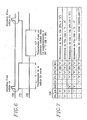
En référence à la Fig. 7, il est considéré une cellule entrante CAe et une cellule sortante CAs et il est montré différents CAs de figure de fonctionnement du circuit de pilote d'anneau 4 en fonction des états des bits FOL et LIB de la cellule entrante CAe et des états des signaux SUP, INF, CT1, CT2, HT et TCV. La notation CAs=CAe(FOL="0") signifie que la cellule sortante transmise CAs est identique à la cellule entrante correspondante CAe excepté le bit FOL qui dans le CAs de la cellule CAs est à l'état "0". La notation CAs=CAe(FOL.LIB="1") indique que pour la cellule sortante les bits FOL et LIB sont tous les deux à l'état "1". La notation CAs="0...0" signifie qu'il est transmis une suite d'état "0" en réponse à l'entrée de la cellule CAe et donc que la cellule CAe est éliminée. Le symbole "-" dans les cases de la table montrée à la Fig. 7 indique que l'état du signal ou bit correspondant est quelconque.With reference to FIG. 7, it is considered an incoming cell CAe and an outgoing cell CAs and it is shown different CAs of the operating figure of the
Claims (5)
Applications Claiming Priority (2)
| Application Number | Priority Date | Filing Date | Title |
|---|---|---|---|
| FR8908762A FR2649269B1 (en) | 1989-06-30 | 1989-06-30 | ADDITIONAL NON-CONNECTION MODE COMMUNICATION SYSTEMS FOR ASYNCHRONOUS TIME NETWORK |
| FR8908762 | 1989-06-30 |
Publications (2)
| Publication Number | Publication Date |
|---|---|
| EP0406077A1 true EP0406077A1 (en) | 1991-01-02 |
| EP0406077B1 EP0406077B1 (en) | 1994-03-30 |
Family
ID=9383309
Family Applications (1)
| Application Number | Title | Priority Date | Filing Date |
|---|---|---|---|
| EP90401783A Expired - Lifetime EP0406077B1 (en) | 1989-06-30 | 1990-06-22 | Complementary connectionless communication system for asynchronous time network |
Country Status (7)
| Country | Link |
|---|---|
| US (1) | US5214648A (en) |
| EP (1) | EP0406077B1 (en) |
| JP (1) | JPH03132123A (en) |
| AU (1) | AU629000B2 (en) |
| CA (1) | CA2020132C (en) |
| DE (1) | DE69007694T2 (en) |
| FR (1) | FR2649269B1 (en) |
Families Citing this family (12)
| Publication number | Priority date | Publication date | Assignee | Title |
|---|---|---|---|---|
| DE69131308T2 (en) * | 1990-08-18 | 2000-01-13 | Toshiba Kawasaki Kk | ATM broadband switching networks with subscriber access units connected by a ring |
| US20020101871A1 (en) | 1991-01-31 | 2002-08-01 | Fujitsu Limited | Connectionless communication system |
| US5392286A (en) * | 1992-08-17 | 1995-02-21 | Matsushita Electric Industrial Co., Ltd. | Data transmission system with packets having occupied, idle, released, and reset states |
| EP0596648A1 (en) | 1992-11-02 | 1994-05-11 | National Semiconductor Corporation | Network link endpoint capability detection |
| USRE39116E1 (en) | 1992-11-02 | 2006-06-06 | Negotiated Data Solutions Llc | Network link detection and generation |
| EP0596651A1 (en) | 1992-11-02 | 1994-05-11 | National Semiconductor Corporation | Network for data communication with isochronous capability |
| USRE39395E1 (en) * | 1992-11-02 | 2006-11-14 | Negotiated Data Solutions Llc | Data communication network with transfer port, cascade port and/or frame synchronizing signal |
| US5533018A (en) | 1994-12-21 | 1996-07-02 | National Semiconductor Corporation | Multi-protocol packet framing over an isochronous network |
| US5648969A (en) * | 1995-02-13 | 1997-07-15 | Netro Corporation | Reliable ATM microwave link and network |
| US5936949A (en) * | 1996-09-05 | 1999-08-10 | Netro Corporation | Wireless ATM metropolitan area network |
| JP3537318B2 (en) | 1998-07-24 | 2004-06-14 | 富士通株式会社 | Switching apparatus and processing method for processing communication data of a specific connection |
| US7058027B1 (en) | 1998-09-16 | 2006-06-06 | Scientific Research Corporation | Systems and methods for asynchronous transfer mode and internet protocol |
Citations (2)
| Publication number | Priority date | Publication date | Assignee | Title |
|---|---|---|---|---|
| US4486877A (en) * | 1982-06-25 | 1984-12-04 | At&T Bell Laboratories | Packet switching loop-around network and facilities testing |
| EP0300606A2 (en) * | 1987-07-22 | 1989-01-25 | Gec-Marconi Limited | Ring shaped local area network |
Family Cites Families (6)
| Publication number | Priority date | Publication date | Assignee | Title |
|---|---|---|---|---|
| JPS61290835A (en) * | 1985-06-19 | 1986-12-20 | Hitachi Ltd | Loop communication system |
| US4751697A (en) * | 1986-09-05 | 1988-06-14 | American Telephone And Telegraph Company, At&T Bell Laboratories | Distributed packet switching sytem |
| FR2625858A1 (en) * | 1988-01-08 | 1989-07-13 | Lmt Radio Professionelle | METHOD AND DEVICE FOR SWITCHING A DATA PACKET |
| CA1294347C (en) * | 1988-05-05 | 1992-01-14 | Man Him Hui | Remote interconnection of local area networks |
| GB8824972D0 (en) * | 1988-10-25 | 1988-11-30 | Plessey Telecomm | Time division switch |
| JP2964151B2 (en) * | 1989-07-03 | 1999-10-18 | 富士通株式会社 | Communication control method |
-
1989
- 1989-06-30 FR FR8908762A patent/FR2649269B1/en not_active Expired - Lifetime
-
1990
- 1990-06-22 DE DE69007694T patent/DE69007694T2/en not_active Expired - Fee Related
- 1990-06-22 EP EP90401783A patent/EP0406077B1/en not_active Expired - Lifetime
- 1990-06-25 US US07/542,826 patent/US5214648A/en not_active Expired - Fee Related
- 1990-06-29 AU AU58033/90A patent/AU629000B2/en not_active Ceased
- 1990-06-29 CA CA002020132A patent/CA2020132C/en not_active Expired - Fee Related
- 1990-06-30 JP JP2174351A patent/JPH03132123A/en active Pending
Patent Citations (2)
| Publication number | Priority date | Publication date | Assignee | Title |
|---|---|---|---|---|
| US4486877A (en) * | 1982-06-25 | 1984-12-04 | At&T Bell Laboratories | Packet switching loop-around network and facilities testing |
| EP0300606A2 (en) * | 1987-07-22 | 1989-01-25 | Gec-Marconi Limited | Ring shaped local area network |
Non-Patent Citations (3)
| Title |
|---|
| BRITISH TELECOMMUNICATIONS ENGINEERING, vol. 6, no. 2, juillet 1987, pages 95-104, Londres, GB; M. LITTLEWOOD et al.: "Network evolution using asynchronous time-division techniques" * |
| IEE PROCEEDINGS SECTION A a I, vol. 131, no. 2, partie E, mars 1984, pages 38-44, Old Woking, GB; R. HULL et al.: "Virtual resource ring: Technique for decentralised resource management in fault-tolerant distributed computer systems" * |
| INTERNATIONAL SWITCHING SYMPOSIUM 1987, Phoenix, 15-20 mars 1987, pages 462-469, IEEE, Phoenix, Arizona, US; M.Wm. BECKNER et al.: "A protocol and prototype for broadband subscriber access to ISDN's" * |
Also Published As
| Publication number | Publication date |
|---|---|
| US5214648A (en) | 1993-05-25 |
| FR2649269B1 (en) | 1991-12-20 |
| EP0406077B1 (en) | 1994-03-30 |
| DE69007694D1 (en) | 1994-05-05 |
| CA2020132C (en) | 1994-10-18 |
| DE69007694T2 (en) | 1994-09-15 |
| JPH03132123A (en) | 1991-06-05 |
| FR2649269A1 (en) | 1991-01-04 |
| AU629000B2 (en) | 1992-09-24 |
| CA2020132A1 (en) | 1990-12-31 |
| AU5803390A (en) | 1991-01-03 |
Similar Documents
| Publication | Publication Date | Title |
|---|---|---|
| EP0609137B1 (en) | Device for cross-mapping between synchronous and asynchronous transmission formats | |
| EP0300876B1 (en) | Hybrid time-division multiplex switching system with an optimized buffer memory | |
| EP0293315B1 (en) | Method and system for controlling the flow of data packets | |
| EP0406077B1 (en) | Complementary connectionless communication system for asynchronous time network | |
| FR2758036A1 (en) | ASYNCHRONOUS CELL TRANSFER MODE SWITCH OF MULTIPLE INPUT CHANNELS WITH MULTIPLE OUTPUT CHANNELS | |
| EP0451029A1 (en) | Connexion circuit switch for through-connecting frames in an asynchronous digital network | |
| FR2758035A1 (en) | ASYNCHRONOUS TRANSFER MODE SWITCH | |
| FR2820921A1 (en) | DEVICE AND METHOD FOR TRANSMISSION IN A SWITCH | |
| EP0383660B1 (en) | Rate reservation in an asynchronous packet network | |
| EP0377203B1 (en) | Reception and processing system for HDLC frames transmitted on PCM-TDM multipaths, especially for a data switcher | |
| FR2804812A1 (en) | METHOD AND DEVICE FOR COMMUNICATION BETWEEN A FIRST AND A SECOND NETWORK | |
| CA2006831C (en) | System with a single hdlc circuit and a conversion buffer memory for transmitting hdlc frames over a pcm channel | |
| EP0340841B1 (en) | Cross-point element between two data highways | |
| EP0715437A1 (en) | Routing method for ATM network | |
| FR2549673A1 (en) | Elementary switch for automatic switching unit using an asynchronous multiplexing technique. | |
| EP0300942B1 (en) | Switching system for data packets with priorities | |
| FR2939992A1 (en) | METHOD FOR BALANCING LATENCY IN A COMMUNICATION SHAFT, DEVICE, COMPUTER PROGRAM PRODUCT, AND CORRESPONDING STORAGE MEDIUM | |
| EP0587468A2 (en) | Photonic connection network with multicast capability | |
| EP0337876B1 (en) | Arrangement for reducing the energy drain of a cyclical working equipment such as a time-multiplexed switcher | |
| EP0689371A1 (en) | Communication system having a network and multiplexing unit | |
| FR2774242A1 (en) | Composite digital word cell asynchronous switching technique | |
| EP0178205B1 (en) | Digital multiple-access network | |
| EP0689319B1 (en) | Routing apparatus for ATM-cells | |
| EP0301934B1 (en) | Time-division switching system for packets of different lengths | |
| EP0752777B1 (en) | ATM connection network |
Legal Events
| Date | Code | Title | Description |
|---|---|---|---|
| PUAI | Public reference made under article 153(3) epc to a published international application that has entered the european phase |
Free format text: ORIGINAL CODE: 0009012 |
|
| AK | Designated contracting states |
Kind code of ref document: A1 Designated state(s): BE DE GB |
|
| 17P | Request for examination filed |
Effective date: 19901130 |
|
| 17Q | First examination report despatched |
Effective date: 19930422 |
|
| RAP1 | Party data changed (applicant data changed or rights of an application transferred) |
Owner name: FRANCE TELECOM |
|
| GRAA | (expected) grant |
Free format text: ORIGINAL CODE: 0009210 |
|
| AK | Designated contracting states |
Kind code of ref document: B1 Designated state(s): BE DE GB |
|
| GBT | Gb: translation of ep patent filed (gb section 77(6)(a)/1977) |
Effective date: 19940329 |
|
| REF | Corresponds to: |
Ref document number: 69007694 Country of ref document: DE Date of ref document: 19940505 |
|
| PG25 | Lapsed in a contracting state [announced via postgrant information from national office to epo] |
Ref country code: BE Effective date: 19940630 |
|
| BERE | Be: lapsed |
Owner name: FRANCE TELECOM Effective date: 19940630 |
|
| PLBE | No opposition filed within time limit |
Free format text: ORIGINAL CODE: 0009261 |
|
| STAA | Information on the status of an ep patent application or granted ep patent |
Free format text: STATUS: NO OPPOSITION FILED WITHIN TIME LIMIT |
|
| 26N | No opposition filed | ||
| REG | Reference to a national code |
Ref country code: GB Ref legal event code: IF02 |
|
| PGFP | Annual fee paid to national office [announced via postgrant information from national office to epo] |
Ref country code: DE Payment date: 20040526 Year of fee payment: 15 |
|
| PGFP | Annual fee paid to national office [announced via postgrant information from national office to epo] |
Ref country code: GB Payment date: 20040602 Year of fee payment: 15 |
|
| PG25 | Lapsed in a contracting state [announced via postgrant information from national office to epo] |
Ref country code: GB Free format text: LAPSE BECAUSE OF NON-PAYMENT OF DUE FEES Effective date: 20050622 |
|
| PG25 | Lapsed in a contracting state [announced via postgrant information from national office to epo] |
Ref country code: DE Free format text: LAPSE BECAUSE OF NON-PAYMENT OF DUE FEES Effective date: 20060103 |
|
| GBPC | Gb: european patent ceased through non-payment of renewal fee |
Effective date: 20050622 |