EP0599665A2 - Detektierschaltung und Detektierverfahren - Google Patents
Detektierschaltung und Detektierverfahren Download PDFInfo
- Publication number
- EP0599665A2 EP0599665A2 EP93309510A EP93309510A EP0599665A2 EP 0599665 A2 EP0599665 A2 EP 0599665A2 EP 93309510 A EP93309510 A EP 93309510A EP 93309510 A EP93309510 A EP 93309510A EP 0599665 A2 EP0599665 A2 EP 0599665A2
- Authority
- EP
- European Patent Office
- Prior art keywords
- signal
- filter
- output
- low
- detecting circuit
- Prior art date
- Legal status (The legal status is an assumption and is not a legal conclusion. Google has not performed a legal analysis and makes no representation as to the accuracy of the status listed.)
- Granted
Links
Images


Classifications
-
- H—ELECTRICITY
- H04—ELECTRIC COMMUNICATION TECHNIQUE
- H04B—TRANSMISSION
- H04B17/00—Monitoring; Testing
- H04B17/10—Monitoring; Testing of transmitters
- H04B17/15—Performance testing
- H04B17/18—Monitoring during normal operation
-
- H—ELECTRICITY
- H04—ELECTRIC COMMUNICATION TECHNIQUE
- H04B—TRANSMISSION
- H04B17/00—Monitoring; Testing
- H04B17/10—Monitoring; Testing of transmitters
- H04B17/101—Monitoring; Testing of transmitters for measurement of specific parameters of the transmitter or components thereof
- H04B17/102—Power radiated at antenna
Definitions
- the present invention relates to a detecting circuit, particularly for detecting a high frequency or radio frequency (RF) signal and, more particularly, to a detecting circuit of the type required to have a linear detection characteristic, as one used to control transmission power in a TDMA (Time Division Multiple Access) communication system.
- the invention also relates to an analogous detection method.
- a detecting circuit of the type described has to meet the following two requirments at the same time when used to detect a TDMA signal or similar RF signal whose power level may change from one time slot to another.
- One requirement is that the mean detection output level of the circuit be maintained smooth in data fields.
- the other requirement is that a transition time existing between nearby time slots be confined in a range which does not affect the mean detection output level.
- a detecting circuit meeting both of these requirements has not been reported yet.
- the present invention therefore seeks to provide a detecting circuit capable of smoothing mean power in each time slot and, at the same time, performing rapid response during each transition time.
- a detecting circuit of the present invention comprises a detector for detecting the envelope of a high frequency signal whose mean power level may change depending on the time slot, and a low-pass filter responsive to a control signal for broadening the pass band for the output of the detector only during the transition time of the mean power level of the high frequency signal.
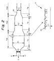
- the detecting circuit includes a detector 3 connected to an amplifier 1.
- the amplifier 1 is provided at the final stage of, for example, a transmitter included in a digital mobile telephone system.
- the amplifier 1 delivers a TDMA signal S1 to an output terminal 2.
- the TDMA signal S1 is an example of transmission signals particular to digital mobile telephones now under development in Japan, as taught in the Journal of the Institute of Electronic Data Communication Engineers of Japan, Vol. 73, No. 8, August 1990.
- the TDMA signal 1 has a data field Td in each time slot TS and has, between nearby time slots TS, a transition time or field Tr beginning at the end of the data field Td of the preceding time slot TS (standardized duration being about 90 ⁇ S).
- the transition time Tr includes a guard time.
- the power level of the TDMA signal 1 differs from one destination to another, i.e., from one time slot TS to another in respect of a mean value P; the data fields Td of the time slots TS1, TS2 and TS3 have mean values P1, P2 and P3, respectively. Further, even in the same data field Td, the instantaneous value changes with the content of data (see FIG 2, portion A).
- the detector 3 shown in FIG. 6 detects the envelope of the TDMA signal 1 and produces an output S2.
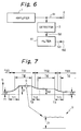
- FIG. 3 shows the levels of the detector output S2. Since the detector 3 lacks the function of limiting the frequency band of the input signal, the time response of the detector output S2 corresponds to the TDMA signal S1. In addition, the above-mentioned mean power P and the detector output level D are proportional to each other.
- the prerequisite with a digital mobile telephone system is that the mean value P of the power level of the TDMA signal S1 be controlled on a time slot TS basis.
- the power level of each data field Td has to be prevented from changing with the content of data.
- a filter 61 FIG. 6, is connected to the output of the detector 3. Specifically, the filter 61 limits the frequency band of the detector output S2 to thereby smooth the detector output level D in each data field Td.
- the resulting output S3 of the filter 61 is delivered to an output terminal 62 as a detection output.
- the filter 61 is implemented as an active filter.
- the detection output S3 eliminates the changes in the detector output level D ascribable to changes in data.
- the signal S3 increases the transition time Tr to the next time slot TS.
- the levels D1 and D2 of the detector output S2 in the time slots TS1 and TS2 are different from each other.
- the transition from the level D1 to the level D2 needs a transition time Tr2 longer than the transition time Tr.
- the transition times Tr1, Tr2 and Tr3 associated with the time slots TS1, TS2 and TS3 are different from each other.
- the mean level D of the detection output S3 is affected, in the data field Td where the detector output level D should remain constant, by the detector output level of the preceding time slot TS. This requires, for example, the data at the detector output level D to be discarded in part of the data field Td. In this manner, the conventional detecting circuit suffers from various limitations in producing an accurate output S3 in each time slot TS.
- the filter 61 smooths the data fields Td of the detector output S2 and, therefore, does not change the cut-off frequency.
- the time constant of the filter 61 will increase and cause the period of time necessary for the transition time Tr to be processed to increase. This causes the transition time Tr to extend into the data field Td of the detector output S2, thereby reducing the period of time available for sampling the data field Td. Consequently, the number of data to be sampled in the data field Td is reduced, forcing a part of the data field Td to be discarded.
- the conventional detecting circuit cannot confine the transition time between nearby time slots in a range which does not affect the mean output level, while maintaining the output level smooth in the data field.
- a detecting circuit embodying the present invention is shown.
- the detecting circuit has a control signal input terminal 4, a pulse generator 5, a filter control 6, a filter 7, and an output terminal 8, in addition to the conventional amplifier 1, detector 3, and output terminal 2.
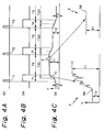
- a control signal S3 has a pulse width of 20 ⁇ S and a period of time slots TS.
- the control signal S3 comes in through the input terminal 4 at times T1, T2 and T3 in synchronism with the beginnings of consecutive transition times Tr.
- the pulse generator 5 generates a pulse signal S4, FIG. 4B, having the same duration (pulse width of 90 ⁇ S) as the transition time Tr every time the control signal S3 arrives.
- the pulse signal S4 is applied to the filter control 6.
- the filter 7 is implemented as a low-pass filter for limiting the frequency band of the output S2 of the detector 3. Specifically, the filter 7 changes the pass band of the detector output S2, i.e., the cut-off frequency fc under the control of the filter control 6. More specifically, when the pulse signal S4 is in a high level (transition time Tr), the filter 7 forms a broad pass band, i.e., raises the cut-off frequency. As a result, a detection output with rapid response, as shown in FIG. 4C, is fed to the output terminal 8. On the other hand, when the pulse signal S4 is in a low level (data field Td), the filter 7 forms a narrow pass band, i.e., lowers the cut-off frequency.
- the filter 7 changes the pass band of the detector output S2, i.e., the cut-off frequency fc under the control of the filter control 6. More specifically, when the pulse signal S4 is in a high level (transition time Tr), the filter 7 forms a broad pass band,
- a detection output S6, FIG. 4C, having a smoothed response is fed out via the output terminal 8.
- the detection output S6 has the level F thereof smoothed and maintained constant without regard to the content of data.
- the output level F follows a change in the power level of the TDMA signal S1 immediately since the filter 7 responds at high speed.
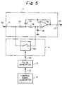
- the filter 7 is an active filter. As shown, the output S2 of the detector 3 is applied to an input terminal 71 included in the filter 7. The signal S2 is routed through resistors 72 and 74 having the same resistance R to the non-inverting input of an operational amplifier 76.
- the operational amplifier 76 has the non-inverting input thereof connected to ground via a capacitor 75 whose capacitance is C2.
- the output terminal of the amplifier 76 is connected to an output terminal 77 on which the detection output S6 appears.
- the detection output S6 is fed back to the inverting input of the amplifier 76 directly and via a capacitor 73 having a capacitance C1 and the resistor 74.
- the filter control 6 is implemented by a switch 60 which is turned on and turned off by the pulse signal S4 applied thereto from the pulse generator 5.
- the switch 60 may be implemented by an IC (Integrated Circuit), e.g., ⁇ PD4538 available from NEC Corporation.
- IC Integrated Circuit
- the switch 60 short-circuits the resistors 72 and 73 of the filter 7. Specifically, since the resistors 72 and 74 are not connected, the time constant of the filter 7 decreases.
- the capacitor 73 discharges when the data field Td changes from a high level to a low level or charges when the data field Td changes from a low level to a high level.
- the filter 7 restores the great time constant.
- the filter 7 produces a detection output S6 having the cut-off frequency represented by the above equation and frequency components of 0 to fc. Since one time slot is 6.7 mS long and the transition time Tr is 90 ⁇ S, the cut-off frequency fc should preferably be about 3 kHz.
- the cut-off frequency of the filter 7 is determined by the cut-off frequency fca of the operational amplifier 7 6 since the resistors 74 and 75 are short-circuited.
- the cut-off frequency fca will respond to the transition time Tr sufficiently if it is higher than 30 kHz.
- control signal S3 applied to the pulse generator 5 is generated by a control signal generator 9, FIG. 5, in synchronism with a host station.
- the preferred embodiment of detecting circuit is capable of smoothing mean power in each time slot and, at the same time, performing rapid response during each transition time.
- the circuit has a detector for detecting the envelope of an RF signal whose power level may change depending on the time slot, and a filter for narrowing the pass band in the data field of each time slot and broadening it in the transition field of the same.
- the output of the detector is applied to the filter.
- the detecting circuit therefore, produces an output which is smoothed in the data field without regard to the content of data and which responds to a change in the power level sharply in the transition field.
Applications Claiming Priority (3)
| Application Number | Priority Date | Filing Date | Title |
|---|---|---|---|
| JP4318716A JPH06164659A (ja) | 1992-11-27 | 1992-11-27 | 検波回路 |
| JP31871692 | 1992-11-27 | ||
| JP318716/92 | 1992-11-27 |
Publications (3)
| Publication Number | Publication Date |
|---|---|
| EP0599665A2 true EP0599665A2 (de) | 1994-06-01 |
| EP0599665A3 EP0599665A3 (de) | 1995-02-15 |
| EP0599665B1 EP0599665B1 (de) | 2000-05-10 |
Family
ID=18102178
Family Applications (1)
| Application Number | Title | Priority Date | Filing Date |
|---|---|---|---|
| EP93309510A Expired - Lifetime EP0599665B1 (de) | 1992-11-27 | 1993-11-29 | Detektierschaltung und Detektierverfahren |
Country Status (6)
| Country | Link |
|---|---|
| US (1) | US5533057A (de) |
| EP (1) | EP0599665B1 (de) |
| JP (1) | JPH06164659A (de) |
| AU (1) | AU668232B2 (de) |
| CA (1) | CA2110149C (de) |
| DE (1) | DE69328607T2 (de) |
Cited By (2)
| Publication number | Priority date | Publication date | Assignee | Title |
|---|---|---|---|---|
| EP0973273A1 (de) * | 1998-07-16 | 2000-01-19 | Alcatel | Verfahren zur Übertragung in aufeinderfolgenden Zeitschlitzen |
| EP1094618A1 (de) * | 1999-10-23 | 2001-04-25 | Siemens Aktiengesellschaft | Verfahren zum Betrieb eines Mobiltelephonsystems |
Families Citing this family (1)
| Publication number | Priority date | Publication date | Assignee | Title |
|---|---|---|---|---|
| CN106603097B (zh) * | 2016-12-31 | 2023-08-18 | 陕西烽火电子股份有限公司 | 一种电台用展宽频响的调制线性化电路 |
Citations (3)
| Publication number | Priority date | Publication date | Assignee | Title |
|---|---|---|---|---|
| US4356567A (en) * | 1977-06-28 | 1982-10-26 | Pioneer Electronic Corporation | Radio receiver with bandwidth switching |
| GB2140235A (en) * | 1983-05-19 | 1984-11-21 | Ates Componenti Elettron | Circuits for reducing noise in electromagnetic wave receivers |
| DE4211549A1 (de) * | 1991-04-09 | 1992-10-15 | Siemens Ag | Verfahren zur rauschunterdrueckung, verwendung und adaptives filter zur durchfuehrung des verfahrens |
Family Cites Families (2)
| Publication number | Priority date | Publication date | Assignee | Title |
|---|---|---|---|---|
| US4495619A (en) * | 1981-10-23 | 1985-01-22 | At&T Bell Laboratories | Transmitter and receivers using resource sharing and coding for increased capacity |
| JPH0779266B2 (ja) * | 1991-04-23 | 1995-08-23 | 国際電気株式会社 | 送信出力制御回路 |
-
1992
- 1992-11-27 JP JP4318716A patent/JPH06164659A/ja active Pending
-
1993
- 1993-11-26 CA CA002110149A patent/CA2110149C/en not_active Expired - Fee Related
- 1993-11-26 AU AU51991/93A patent/AU668232B2/en not_active Ceased
- 1993-11-29 DE DE69328607T patent/DE69328607T2/de not_active Expired - Fee Related
- 1993-11-29 US US08/158,701 patent/US5533057A/en not_active Expired - Fee Related
- 1993-11-29 EP EP93309510A patent/EP0599665B1/de not_active Expired - Lifetime
Patent Citations (3)
| Publication number | Priority date | Publication date | Assignee | Title |
|---|---|---|---|---|
| US4356567A (en) * | 1977-06-28 | 1982-10-26 | Pioneer Electronic Corporation | Radio receiver with bandwidth switching |
| GB2140235A (en) * | 1983-05-19 | 1984-11-21 | Ates Componenti Elettron | Circuits for reducing noise in electromagnetic wave receivers |
| DE4211549A1 (de) * | 1991-04-09 | 1992-10-15 | Siemens Ag | Verfahren zur rauschunterdrueckung, verwendung und adaptives filter zur durchfuehrung des verfahrens |
Cited By (4)
| Publication number | Priority date | Publication date | Assignee | Title |
|---|---|---|---|---|
| EP0973273A1 (de) * | 1998-07-16 | 2000-01-19 | Alcatel | Verfahren zur Übertragung in aufeinderfolgenden Zeitschlitzen |
| FR2781323A1 (fr) * | 1998-07-16 | 2000-01-21 | Alsthom Cge Alcatel | Procede de transmission dans des fenetres successives |
| US6606308B1 (en) | 1998-07-16 | 2003-08-12 | Alcatel | Method of transmitting in successive time slots |
| EP1094618A1 (de) * | 1999-10-23 | 2001-04-25 | Siemens Aktiengesellschaft | Verfahren zum Betrieb eines Mobiltelephonsystems |
Also Published As
| Publication number | Publication date |
|---|---|
| AU668232B2 (en) | 1996-04-26 |
| DE69328607D1 (de) | 2000-06-15 |
| EP0599665B1 (de) | 2000-05-10 |
| CA2110149C (en) | 1997-06-10 |
| CA2110149A1 (en) | 1994-05-28 |
| EP0599665A3 (de) | 1995-02-15 |
| AU5199193A (en) | 1994-06-09 |
| US5533057A (en) | 1996-07-02 |
| JPH06164659A (ja) | 1994-06-10 |
| DE69328607T2 (de) | 2001-02-01 |
Similar Documents
| Publication | Publication Date | Title |
|---|---|---|
| US5408197A (en) | Automatic power control circuit for controlling transmitting power of modulated radio frequency signal | |
| EP0414352B1 (de) | Funksender mit Ausgangsleistungssteuerung | |
| EP0654898B1 (de) | Übertragungsschaltung | |
| EP0135081B1 (de) | Störpegelreduzierung durch lineare Interpolation unter Verwendung einer Verstärkerschaltung mit doppelter Funktion | |
| EP0594153A2 (de) | Schaltung zur Leistungssteurerung eines digitalen Funktelefons | |
| US4847523A (en) | Lock-in test amplifier | |
| EP0599665B1 (de) | Detektierschaltung und Detektierverfahren | |
| EP0051472A1 (de) | Einseiten-Bandempfänger | |
| JPH06167517A (ja) | コンパレータ回路 | |
| JP3463727B2 (ja) | クロックパルス伝送回路 | |
| EP0534484B1 (de) | Schaltung für Impulsleistungsverstärker, dessen Ausgangssignal die erwünschte Kurvenform hat | |
| US4458209A (en) | Adaptive power control circuit | |
| US4219745A (en) | Backlash filter apparatus | |
| EP0383271B1 (de) | Schaltung zur Wellenformung und Empfänger, der diese Schaltung benutzt | |
| US5212829A (en) | Circuit arrangement for suppression of interference signals | |
| WO2003065668A1 (en) | Fast settling data slicer comprising a low-pass filter with switchable cut-off frequency and a notch-filter | |
| EP0515102A2 (de) | Automatische Verlustkontrolleschaltung in einem schleifenförmigen digitalen Übertragungssystem | |
| US5909143A (en) | Circuit for determining and storing an average signal value | |
| US5630219A (en) | Reception electric field level detection circuit | |
| US5712475A (en) | Light receiving circuit with variable threshold circuit | |
| CN1360751A (zh) | 校正有用信号失真的方法和装置 | |
| JPH0326121A (ja) | 周波数変調パネルの非実装時の変調度制御回路 | |
| JP3479369B2 (ja) | ノイズ除去機能を持つ受信装置 | |
| KR200210073Y1 (ko) | 전력 검출부의 바이어스 전압 안정화 회로 | |
| US7154954B1 (en) | Communication system |
Legal Events
| Date | Code | Title | Description |
|---|---|---|---|
| PUAI | Public reference made under article 153(3) epc to a published international application that has entered the european phase |
Free format text: ORIGINAL CODE: 0009012 |
|
| AK | Designated contracting states |
Kind code of ref document: A2 Designated state(s): DE FR GB NL SE |
|
| PUAL | Search report despatched |
Free format text: ORIGINAL CODE: 0009013 |
|
| AK | Designated contracting states |
Kind code of ref document: A3 Designated state(s): DE FR GB NL SE |
|
| 17P | Request for examination filed |
Effective date: 19950118 |
|
| 17Q | First examination report despatched |
Effective date: 19990326 |
|
| GRAG | Despatch of communication of intention to grant |
Free format text: ORIGINAL CODE: EPIDOS AGRA |
|
| GRAG | Despatch of communication of intention to grant |
Free format text: ORIGINAL CODE: EPIDOS AGRA |
|
| GRAH | Despatch of communication of intention to grant a patent |
Free format text: ORIGINAL CODE: EPIDOS IGRA |
|
| GRAH | Despatch of communication of intention to grant a patent |
Free format text: ORIGINAL CODE: EPIDOS IGRA |
|
| GRAA | (expected) grant |
Free format text: ORIGINAL CODE: 0009210 |
|
| AK | Designated contracting states |
Kind code of ref document: B1 Designated state(s): DE FR GB NL SE |
|
| PG25 | Lapsed in a contracting state [announced via postgrant information from national office to epo] |
Ref country code: NL Free format text: LAPSE BECAUSE OF FAILURE TO SUBMIT A TRANSLATION OF THE DESCRIPTION OR TO PAY THE FEE WITHIN THE PRESCRIBED TIME-LIMIT Effective date: 20000510 |
|
| REF | Corresponds to: |
Ref document number: 69328607 Country of ref document: DE Date of ref document: 20000615 |
|
| PG25 | Lapsed in a contracting state [announced via postgrant information from national office to epo] |
Ref country code: SE Free format text: LAPSE BECAUSE OF FAILURE TO SUBMIT A TRANSLATION OF THE DESCRIPTION OR TO PAY THE FEE WITHIN THE PRESCRIBED TIME-LIMIT Effective date: 20000810 |
|
| ET | Fr: translation filed | ||
| NLV1 | Nl: lapsed or annulled due to failure to fulfill the requirements of art. 29p and 29m of the patents act | ||
| PLBE | No opposition filed within time limit |
Free format text: ORIGINAL CODE: 0009261 |
|
| STAA | Information on the status of an ep patent application or granted ep patent |
Free format text: STATUS: NO OPPOSITION FILED WITHIN TIME LIMIT |
|
| 26N | No opposition filed | ||
| REG | Reference to a national code |
Ref country code: GB Ref legal event code: IF02 |
|
| PGFP | Annual fee paid to national office [announced via postgrant information from national office to epo] |
Ref country code: FR Payment date: 20021108 Year of fee payment: 10 |
|
| PGFP | Annual fee paid to national office [announced via postgrant information from national office to epo] |
Ref country code: GB Payment date: 20021127 Year of fee payment: 10 |
|
| PGFP | Annual fee paid to national office [announced via postgrant information from national office to epo] |
Ref country code: DE Payment date: 20021205 Year of fee payment: 10 |
|
| PG25 | Lapsed in a contracting state [announced via postgrant information from national office to epo] |
Ref country code: GB Free format text: LAPSE BECAUSE OF NON-PAYMENT OF DUE FEES Effective date: 20031129 |
|
| PG25 | Lapsed in a contracting state [announced via postgrant information from national office to epo] |
Ref country code: DE Free format text: LAPSE BECAUSE OF NON-PAYMENT OF DUE FEES Effective date: 20040602 |
|
| GBPC | Gb: european patent ceased through non-payment of renewal fee |
Effective date: 20031129 |
|
| PG25 | Lapsed in a contracting state [announced via postgrant information from national office to epo] |
Ref country code: FR Free format text: LAPSE BECAUSE OF NON-PAYMENT OF DUE FEES Effective date: 20040730 |
|
| REG | Reference to a national code |
Ref country code: FR Ref legal event code: ST |