EP0596714B1 - Festkörperlaser - Google Patents
Festkörperlaser Download PDFInfo
- Publication number
- EP0596714B1 EP0596714B1 EP93308775A EP93308775A EP0596714B1 EP 0596714 B1 EP0596714 B1 EP 0596714B1 EP 93308775 A EP93308775 A EP 93308775A EP 93308775 A EP93308775 A EP 93308775A EP 0596714 B1 EP0596714 B1 EP 0596714B1
- Authority
- EP
- European Patent Office
- Prior art keywords
- optical element
- optical
- birefringent
- solid state
- state laser
- Prior art date
- Legal status (The legal status is an assumption and is not a legal conclusion. Google has not performed a legal analysis and makes no representation as to the accuracy of the status listed.)
- Expired - Lifetime
Links
Images


Classifications
-
- H—ELECTRICITY
- H01—ELECTRIC ELEMENTS
- H01S—DEVICES USING THE PROCESS OF LIGHT AMPLIFICATION BY STIMULATED EMISSION OF RADIATION [LASER] TO AMPLIFY OR GENERATE LIGHT; DEVICES USING STIMULATED EMISSION OF ELECTROMAGNETIC RADIATION IN WAVE RANGES OTHER THAN OPTICAL
- H01S3/00—Lasers, i.e. devices using stimulated emission of electromagnetic radiation in the infrared, visible or ultraviolet wave range
- H01S3/10—Controlling the intensity, frequency, phase, polarisation or direction of the emitted radiation, e.g. switching, gating, modulating or demodulating
- H01S3/106—Controlling the intensity, frequency, phase, polarisation or direction of the emitted radiation, e.g. switching, gating, modulating or demodulating by controlling devices placed within the cavity
- H01S3/108—Controlling the intensity, frequency, phase, polarisation or direction of the emitted radiation, e.g. switching, gating, modulating or demodulating by controlling devices placed within the cavity using non-linear optical devices, e.g. exhibiting Brillouin or Raman scattering
- H01S3/109—Frequency multiplication, e.g. harmonic generation
-
- H—ELECTRICITY
- H01—ELECTRIC ELEMENTS
- H01S—DEVICES USING THE PROCESS OF LIGHT AMPLIFICATION BY STIMULATED EMISSION OF RADIATION [LASER] TO AMPLIFY OR GENERATE LIGHT; DEVICES USING STIMULATED EMISSION OF ELECTROMAGNETIC RADIATION IN WAVE RANGES OTHER THAN OPTICAL
- H01S3/00—Lasers, i.e. devices using stimulated emission of electromagnetic radiation in the infrared, visible or ultraviolet wave range
- H01S3/05—Construction or shape of optical resonators; Accommodation of active medium therein; Shape of active medium
- H01S3/06—Construction or shape of active medium
- H01S3/0602—Crystal lasers or glass lasers
- H01S3/0604—Crystal lasers or glass lasers in the form of a plate or disc
-
- H—ELECTRICITY
- H01—ELECTRIC ELEMENTS
- H01S—DEVICES USING THE PROCESS OF LIGHT AMPLIFICATION BY STIMULATED EMISSION OF RADIATION [LASER] TO AMPLIFY OR GENERATE LIGHT; DEVICES USING STIMULATED EMISSION OF ELECTROMAGNETIC RADIATION IN WAVE RANGES OTHER THAN OPTICAL
- H01S3/00—Lasers, i.e. devices using stimulated emission of electromagnetic radiation in the infrared, visible or ultraviolet wave range
- H01S3/05—Construction or shape of optical resonators; Accommodation of active medium therein; Shape of active medium
- H01S3/06—Construction or shape of active medium
- H01S3/0627—Construction or shape of active medium the resonator being monolithic, e.g. microlaser
-
- H—ELECTRICITY
- H01—ELECTRIC ELEMENTS
- H01S—DEVICES USING THE PROCESS OF LIGHT AMPLIFICATION BY STIMULATED EMISSION OF RADIATION [LASER] TO AMPLIFY OR GENERATE LIGHT; DEVICES USING STIMULATED EMISSION OF ELECTROMAGNETIC RADIATION IN WAVE RANGES OTHER THAN OPTICAL
- H01S3/00—Lasers, i.e. devices using stimulated emission of electromagnetic radiation in the infrared, visible or ultraviolet wave range
- H01S3/05—Construction or shape of optical resonators; Accommodation of active medium therein; Shape of active medium
- H01S3/08—Construction or shape of optical resonators or components thereof
- H01S3/08018—Mode suppression
- H01S3/0804—Transverse or lateral modes
- H01S3/0805—Transverse or lateral modes by apertures, e.g. pin-holes or knife-edges
-
- H—ELECTRICITY
- H01—ELECTRIC ELEMENTS
- H01S—DEVICES USING THE PROCESS OF LIGHT AMPLIFICATION BY STIMULATED EMISSION OF RADIATION [LASER] TO AMPLIFY OR GENERATE LIGHT; DEVICES USING STIMULATED EMISSION OF ELECTROMAGNETIC RADIATION IN WAVE RANGES OTHER THAN OPTICAL
- H01S3/00—Lasers, i.e. devices using stimulated emission of electromagnetic radiation in the infrared, visible or ultraviolet wave range
- H01S3/05—Construction or shape of optical resonators; Accommodation of active medium therein; Shape of active medium
- H01S3/08—Construction or shape of optical resonators or components thereof
- H01S3/08054—Passive cavity elements acting on the polarization, e.g. a polarizer for branching or walk-off compensation
-
- H—ELECTRICITY
- H01—ELECTRIC ELEMENTS
- H01S—DEVICES USING THE PROCESS OF LIGHT AMPLIFICATION BY STIMULATED EMISSION OF RADIATION [LASER] TO AMPLIFY OR GENERATE LIGHT; DEVICES USING STIMULATED EMISSION OF ELECTROMAGNETIC RADIATION IN WAVE RANGES OTHER THAN OPTICAL
- H01S3/00—Lasers, i.e. devices using stimulated emission of electromagnetic radiation in the infrared, visible or ultraviolet wave range
- H01S3/05—Construction or shape of optical resonators; Accommodation of active medium therein; Shape of active medium
- H01S3/08—Construction or shape of optical resonators or components thereof
- H01S3/08059—Constructional details of the reflector, e.g. shape
- H01S3/08063—Graded reflectivity, e.g. variable reflectivity mirror
-
- H—ELECTRICITY
- H01—ELECTRIC ELEMENTS
- H01S—DEVICES USING THE PROCESS OF LIGHT AMPLIFICATION BY STIMULATED EMISSION OF RADIATION [LASER] TO AMPLIFY OR GENERATE LIGHT; DEVICES USING STIMULATED EMISSION OF ELECTROMAGNETIC RADIATION IN WAVE RANGES OTHER THAN OPTICAL
- H01S3/00—Lasers, i.e. devices using stimulated emission of electromagnetic radiation in the infrared, visible or ultraviolet wave range
- H01S3/14—Lasers, i.e. devices using stimulated emission of electromagnetic radiation in the infrared, visible or ultraviolet wave range characterised by the material used as the active medium
- H01S3/16—Solid materials
- H01S3/163—Solid materials characterised by a crystal matrix
- H01S3/1671—Solid materials characterised by a crystal matrix vanadate, niobate, tantalate
- H01S3/1673—YVO4 [YVO]
Definitions
- the present invention relates to a solid state laser apparatus for use as a light source in such fields as optical recording, communication and measurement.
- Fig. 23(a) is a front view showing a structure of conventional solid state laser apparatus.
- the solid state laser apparatus comprises a light source emitting a pumping radiation 66 for exciting a lasant material 62, a lens system 61 for focusing of the pumping radiation 66 and an optical resonator 65 comprising the lasant material 62, a non-linear optical element 63 and a concave mirror 64, which are disposed on an optical axis 68.
- the lasant material 62 is formed of Nd:YVO 4 doped with about 1% of Nd, which is a positive uniaxial crystal
- the non-linear optical element 63 is formed of KTiOPO 4 which is a positive biaxial crystal
- a semiconductor laser of 809 nm in oscillatory wavelength is employed as the light source 60.
- the pumping radiation 66 from the light source 60 is focused by the lens system 61, and enters the lasant material 62, an inverted distribution is formed in the lasant material 62, thus, in the case of Nd:YVO 4 crystal, a light amplification of 1064 nm in wavelength is allowed.
- a surface 62a of lasant material 62 is coated with a coating which has a high transmissivity at a wavelength of 809 nm that corresponds to the pumping radiation 66 and a high reflectance at a wavelength of 1064 nm, while a surface 64a of the concave mirror 64 is coated with a coating which has a high transmissivity at a wavelength of 532 nm and a high reflectance at a wavelength of 1064 nm, so that an optical resonator at a wavelength of 1064 nm is formed of the two surfaces 62a and 64a.
- a laser beam of 1064 nm in wavelength oscillated by a light amplifying effect of the laser material 62 passes through the non-linear optical element 63, it is converted to 532 nm in wavelength, which corresponds to a second harmonic, and an output beam 67 is obtained.
- surfaces 63a and 63b of the non-linear optical element 63 are coated with coatings which have a high transmissivity at wavelengths of 1064 and 532 nm, while a surface 62b of the lasant material 62 is coated with a coating which has a high transmissivity at a wavelength of 1064 nm.
- Fig. 23 (b) is a partial perspective view showing an arrangement of polarization axes of the lasant material 62 and the non-linear optical element 63 shown in Fig. 23(a).
- Nd:YVO 4 forming the lasant material 62 is a positive uniaxial crystal
- a principal index of refraction nc is higher than two other principal indices of refraction na
- a c-axis that is an oscillation facilitating axis is directed vertically upwardly to the optical axis 68
- an a-axis of the principal indices of refraction na is positioned so as to coincide with the optical axis 68.
- the non-linear optical element 63 is controlled by temperature adjustment or the like, so that a phase difference by one-way retardation at a specified wavelength of longitudinal mode comes to be m ⁇ (where m is an integer), polarization in the lasant material 62 is maintained in a linear polarization parallel with the c-axis, the oscillation facilitating axis.
- the output beam 67 is emitted to the outside as a coherent light of 532 nm in wavelength through the concave mirror 64, because a laser beam of 1064 nm in wavelength enclosed within the optical resonator is harmonically converted in the non-linear optical element 63 in so-called type II phase matching condition, where a second harmonic is produced by existence of fundamental waves linearly polarized in the z-and y-axes.
- a laser with Nd x Y 1-x Al 3 (BO 3 ) 4 employed as a lasant material is disclosed in Japanese Laid-Open Patents (KOKAI) No. 91-174786 and 91-88380, wherein a beam walk-off is caused in the lasant material, and a laser oscillation is initiated along the oscillation facilitating axis.
- Optics Letters, vol. 16, no. 21, 01/11/91, pages 1665-1667 (D1), US-A-5 130 997 (D2), Patent Abstracts of Japan, vol. 14, no. 396 (E-970) (4339), 27/08/90 (D3) and EP-A-0 508 406 (D4) give examples of apparatuses in which an intracavity non-linear crystal generates the second harmonic of the fundamental frequency of a laser resonant cavity.
- D1, D2 and D4 disclose use of KTiOPO 4 (KTP) as the non-linear material.
- D2 and D3 illustrate arrangements by which power loss caused by beam walk-off in the non-linear crystal may be reduced by recombining the separated beams.
- the present invention provides a solid state laser apparatus comprising an optical resonator including a plurality of elements, one of the optical elements being a lasant material to be excited by generated pumping radiation and at least two of the optical elements being birefringent optical elements, said optical resonator having a single optical axis formed by one of two polarizing optical axes separated by a beam walk-off caused in a first one of the birefringent optical elements.
- the optical resonator is of a linear type
- at least one of reflecting mirror means composing the optical resonator is curved mirror means
- the first birefringent optical element is placed between the curved mirror means and a second birefringent optical element.
- the reflecting mirror means may be a coating layer with a high reflectance at a specified wavelength coated on a surface of the optical element or a mirror independently positioned.
- the optical resonator is of a linear type
- at least one of reflecting mirror means composing the optical resonator is flat mirror means
- a second birefringent optical element other than the first birefringent optical element is placed between the flat mirror means and the first birefringent optical element.
- the lasant material is the first birefringent optical element.
- curved reflecting mirror means composing the optical resonator the lasant material providing the first birefringent optical element, at least one of the second birefringent optical elements and reflecting mirror means composing the optical resonator are placed in the order from an incident side of the pumping radiation, and a beam walk-off is caused in the lasant material.
- the lasant material is formed of Nd:YVO 4 .
- At least one of the second birefringent optical elements is formed of a non-linear optical material and a laser beam oscillated by the lasant material is converted to a second harmonic by the non-linear optical material.
- the nonlinear optical material is formed of KTiOPO 4 .
- curved mirror means composing the optical resonator, the lasant material, the first birefringent optical element, the second birefringent optical element and flat mirror means composing the optical resonator are placed in the order from an incident side of the pumping radiation, and a beam walk-off is caused also in the second birefringent optical element.
- the lasant material is the second birefringent optical element.
- reflecting mirror means composing the optical resonator the lasant material providing the second birefringent optical element, the first birefringent optical element and curved mirror means composing the optical resonator are placed in the order from an incident side of the pumping radiation.
- the first birefringent optical element is formed of a non-linear optical material, and a laser beam oscillated by the lasant material is converted to a second harmonic by the non-linear optical material.
- reflecting mirror means composing the optical resonator, the lasant material, the second birefringent optical element, the first birefringent optical element and curved mirror means composing the optical resonator are placed in the order from an incident side of the pumping radiation.
- the lasant material is formed of Nd:YAG.
- the first birefringent optical element is formed of a non-linear optical material, and a laser beam oscillated by the lasant material is converted to a second harmonic by the non-linear optical material.
- the non-linear optical material is formed of KNbO 3 .
- a beam walk-off with wave number vector and Poynting's vector of light mutually different in direction from each other is caused in a birefringent optical element, as an optical resonator is formed for one of two polarizing optical axes separated by the beam walk-off, a resonance loss with respect to the other polarizing optical axis is increased, discrimination by polarizing mode is enabled, and an output variation due to a longitudinal mode hopping is suppressed.
- the invention can provide a solid state laser apparatus capable of suppressing the mode-hop phenomenon, allowing oscillation in a single longitudinal mode, and providing a very stable output beam by increasing a resonance loss in longitudinal modes except a fundamental mode.
- an optical resonator 6 comprises a first birefringent optical element 1, second birefringent optical element 2, lasant material 3 without birefringent property and reflecting mirrors 4 and 5, by making use of an optical anisotropy of the first birefringent optical element 1, a beam walk-off is generated in a beam passing therethrough, and an optical axis of the optical resonator 6 is formed by only one optical axis 7 of two polarizing optical axes 7 and 8 separated by the beam walk-off.
- a surface 1a on the side of lasant material 3 of the first birefringent optical element 1 when X-axis perpendicular to the optical axis 7 (in the forward direction of the sheet of of Fig. 1 (a)) and Y-axis (in the upward direction of the sheet of Fig. 1 (a)) are established, as shown in Fig. 1 (b), the direction of polarizing axis of the first birefringent optical element 1 for a beam on the optical axis 7 is designed to be parallel with the Y-axis.
- polarizing axes of the first and second birefringent optical elements 1 and 2 are within a plane perpendicular to the optical axis 7, and form an angle 45° between them.
- the direction of polarization of a beam related to laser oscillation, originated in the surface la on the side of lasant material 3 of the first birefringent optical element 1, passing through the first birefringent optical element 1, and transmitted to a surface 1b is parallel with the Y-axis.
- the longitudinal mode corresponding to the polarizing mode of the direction p3 parallel with the Y-axis of the first birefringent optical element is dominantly provided for oscillation, mode hopping to the other longitudinal modes is suppressed, and an output variation is reduced.
- ⁇ ( ⁇ 1/2 ) ⁇ 0 ⁇ ⁇ (1/2) ⁇ 2 ⁇ ⁇ FSR cav /FSR pol ⁇
- the second birefringent optical element 2 serves for separating polarizations corresponding to the longitudinal modes in the optical resonator, and the first birefringent optical element 1 serves for discriminating only one mode of the seperated polarizations by means of a beam walk-off.
- the second birefringent optical element 2 is not required to comprise a single element, and may be a combination of plural birefringent optical elements capable of serving for separating polarizing modes according to the longitudinal modes. In other words, although such case with two birefringent optical elements has been described, generally, even when three or more birefringent optical elements are increased, only one longitudinal mode can be discriminated by optical anisotropy and beam walk-off in the birefringent optical elements.
- the optical resonator is of a linear type
- at least one of reflecting mirror means composing the optical resonator is the curved mirror means
- the first birefringent optical element is placed between the curved mirror means and a second birefringent optical element other than the first birefringent optical element, a light deviating from an optical axis of the optical resonator is reflected outside the optical axis, and a resonance loss is surely caused for the other polarizing optical axis.
- a mirror 4 of the optical resonator is a flat mirror, as a light along two polarizing optical axes 7 and 8 separated by a beam walk-off that in the first birefringent optical element 1 is reflected as it is to the opposite direction, and the optical axes are matched, the optical resonator is formed for the two polarizing optical axes 7 and 8. Therefore, in order to increase a resonance loss with respect to the other polarizing optical axis 8, as shown in Fig. 1, a curved mirror is preferably provided as the mirror 4 with more spacing between the two polarizing optical axes 7 and 8 because of a beam walk-off for mode discrimination.
- the optical resonator is of a linear type, at least one of reflecting mirror means composing the optical resonator is flat mirror means, and a second birefringent optical element other than the first birefringent optical element is placed between the flat mirror means and the first birefringent optical element, even when a beam walk-off without a purpose of mode discrimination is caused, the optical resonator is formed for two polarizing optical axes separated by the beam walk-off.
- the radius ⁇ of transverse mode in an electric field is a distance where an amplitude of electric field of a Gaussian beam comes to be 1/e (where e is a base of natural logarithm) of a value at a central axis of the beam (A. Yariv: Quantum Electronics, 2nd ed., p.112, Wiley).
- a pumping radiation 10 for exciting the lasant material 3 enters along the optical axis 7, and a excited area having a spot with a radius equal to or less than a beam radius of the light beam 7a is formed in the lasant material 3.
- coaxial excitation method such arrangement of directing a pumping radiation so as to be coincident with the optical axis 7 of optical resonator 6 is generally referred to as coaxial excitation method.
- d1 L ⁇ tan ⁇ ⁇ ⁇
- d1 is a spacing between the optical axes 7 and 8 at a position of exit from the first birefringent optical element
- ⁇ is a beam radius of the light beam 7a along the optical axis 7 inside the lasant material 3
- ⁇ is a beam walk-off angle in the first birefringent optical element 1
- L is a length of material of the first birefringent optical element 1, thus the laser oscillation of the light beam 8a along the optical axis 8 is suppressed, and the mode discrimination can be easily achieved.
- the concept is applicable also to so-called side excitation method, in which a pumping radiation 10 is allowed to enter from the direction perpendicular to an optical axis 7 of optical resonator 6 as shown in Fig. 5 (b).
- a first birefringent optical element 1 also serves as a lasant material 3, and laser oscillation of a light beam 8a is not effected, if the light beam 8a is not reflected by a mirror 4, even when the light beam 8a is separated by a beam walk-off.
- d2 L ⁇ tan ⁇ ⁇ r/N
- d2 is a spacing between optical axes 7 and 8 on the mirror 4
- r is an effective aperture radius of the mirror 4
- ⁇ is a beam walk-off angle in the first birefringent optical element 1
- L is a length of material of the first birefringent optical element 1, thus laser oscillation of the light beam 8a along the optical axis 8 is suppressed, and the mode discrimination is achieved.
- N is desired to be set at 10, more preferably 5.
- Such concept of limiting an aperture of resonator can be also achieved by such methods as (1) forming a mask 11 in an area outside an effective aperture of the mirror 4, as shown in Fig. 7; (2) inserting a diaphragm 12 between the first birefringent optical element 1 and mirror 4, as shown in Fig. 8; or (3) forming a small curved portion 1c in a surface of the first birefringent optical element 1 by utilizing such fine processing technology as photolithography to integrally provide a mirror composing an optical resonator (Japanese Patent Application No. 92-161407),as shown in Fig. 9. Furthermore, as shown in Fig.
- diaphragms 12a and 12b may be inserted between the lasant material 3 in which a beam walk-off is generated and mirror 4, and the lasant material 3 and first birefringent optical element 1, respectively, for preventing laser oscillation along the optical axis 8.
- the effective aperture radius means a radius of a circular surface area in the reflecting mirror that is capable of smoothly reflecting a laser beam without causing any distortion in a wave front.
- a laser material serves as a first birefringent optical element
- a laser oscillation is dominantly effected on one optical axis of two polarizing optical axes generated in the first birefringent optical element.
- a polarizing optical axis cannot be selected only by such physical arrangement, an ordinary and extraordinary rays generated in the first birefringent optical element out of lights directed toward the mirror 5 are separated on a surface 1a, and one of them is advanced along a polarizing optical axis 7, and the other along a polarizing optical axis 13.
- Oscillation at such wavelength that a phase difference ⁇ due to retardation in a second birefringent optical element 2 is, for example, m ⁇ and n ⁇ (where m and n are integers close to each other) is possibly present in the two polarizing axes simultaneously.
- an optical axis of optical resonator is matched with an optical axis of ordinary ray in a first birefringent optical element
- discrimination of longitudinal modes can be also achieved in a similar manner by matching the optical axis of optical resonator with an optical axis of extraordinary ray in the first birefringent optical element.
- a light source emitting a pumping radiation is a semiconductor laser
- an entire solid state laser apparatus can be reduced in size and weight.
- the mode hopping phenomenon to other longitudinal mode is suppressed, since longitudinal modes are discriminated by means of not only an oscillation facilitating axis of lasant material but also separation of two polarizing optical axes by beam walk-off, so that a very stable output with less variation can be obtained.
- Fig. 1 (a) shows a principle of the invention
- Fig. 1 (b) a polarizing mode of longitudinal mode in an optical resonator.
- Fig. 2 is a block diagram showing a part of a solid state laser apparatus with a flat mirror employed for mirror 4, and a curved mirror for mirror 5.
- Fig. 3 is a block diagram showing a part of a solid state laser apparatus with curved mirrors employed for mirrors 4 and 5.
- Fig. 4 is a block diagram showing a part of a solid state laser apparatus with a curved mirror employed for mirror 4, and a flat mirror for mirror 5.
- Fig. 5 (a) is a partial block diagram showing a beam in Fig. 1 (a), and Fig. 5 (b) a partial perspective view illustrating an example of lasant material 3 in side excitation.
- Fig. 6 is a block diagram of a part of a solid state laser apparatus, illustrating an example of separation of a light beam.
- Fig. 7 is a block diagram of a part of a solid state laser apparatus, illustrating another example of separation of a light beam.
- Fig. 8 is a block diagram of a part of a solid state laser apparatus, illustrating other example of separation of a light beam.
- Fig. 9 is a block diagram of a part of a solid state laser apparatus, illustrating still other example of separation of a light beam.
- Fig. 10 is a block diagram of a part of a solid state laser apparatus, illustrating further example of separation of a light beam.
- Fig. 11 is a partial block diagram showing discrimination of polarization modes by utilizing a birefringent property of a lasant material.
- Fig. 12 (a) is a front view showing a structure of a solid state laser apparatus of a first embodiment according to the invention, and Fig. 12 (b) a graph showing a polarizing mode in a surface 24a of a non-linear optical element 24.
- Figs. 13(a) and (b) are graphs showing changes of a beam walk-off angle ⁇ and laser gain G of a lasant material 23 in relation to an inclination ⁇ of c-axis.
- Fig. 14 (a) is a front view showing a structure of a solid state laser apparatus of a second embodiment according to the invention
- Fig. 14 (b) a partial perspective view showing a position of polarizing axis of a non-linear optical element 24 thereof
- Fig. 14 (c) a graph showing a polarizing mode on a surface 24a of the non-linear optical element 24.
- Fig. 15 (a) is a front view showing a structure of a solid state laser apparatus of a third embodiment according to the invention, and Fig. 15 (b) a view showing an arrangement of polarizing axis of a non-linear optical element 24.
- Fig. 16 is a graph showing a KTP temperature dependency of wavelength in laser oscillation in a solid state laser apparatus of the third embodiment according to the invention.
- Fig. 17 is a graph showing a KTP temperature dependency of RIN in a solid state laser apparatus of the third embodiment according to the invention.
- Fig. 18 is a front view showing a structure of a solid state laser apparatus of a fourth embodiment according to the invention.
- Fig. 19 is a graph showing a KTP temperature dependency of wavelength in laser oscillation in a solid state laser apparatus of the fourth embodiment according to the invention.
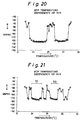
- Fig. 20 is a graph showing a KTP temperature dependency of RIN in a solid state laser apparatus of the fourth embodiment according to the invention.
- Fig. 21 is a graph showing a KTP temperature dependency of RIN in a solid state laser apparatus of a fifth embodiment according to the invention.
- Fig. 22 (a) is a front view showing a structure of a solid state laser apparatus of a sixth embodiment according to the invention, Fig. 22 (b) a coordinate system showing the cutting direction of a non-linear optical element 24, Fig. 22 (c) a partial perspective view showing the polarizing direction of pumping radiation 26 in Fig. 22 (a) and an arrangement of a polarizing axis of a birefringent optical element 41 and the non-linear optical element 24, and Fig. 22 (d) a graph showing a polarizing mode on a surface 24a of the non-linear optical element 24.
- Fig. 23 (a) is a front view showing an example of structure of a conventional solid state laser apparatus
- Fig. 23 (b) a partial perspective view showing an arrangement of a polarizing axis of a lasant material 62 and non-linear optical element 63
- Fig. 23 (c) a coordinate system explaining the cutting direction of the non-linear optical element 63.
- Fig. 12 (a) is a front view showing a structure of a solid state laser apparatus of a first embodiment according to the invention.
- the solid state laser apparatus comprises such components as a semiconductor laser (SLD 303 WT-25 supplied by SONY) 20 emitting a pumping radiation 26 for excitating of a lasant material 23, lens systems 21a and 21b (F-L20 supplied by New Port) for focusing the pumping radiation 26 and an optical resonator 25 comprising the lasant material 23 formed of Nd:YVO 4 doped with approximately 1 % of Nd and a non-linear optical element 24 formed of KTiOPO 4 , wherein a surface 23b of the lasant material 23 is in contact with a surface 24a of the non-linear optical element 24.
- a semiconductor laser SLD 303 WT-25 supplied by SONY
- lens systems 21a and 21b F-L20 supplied by New Port
- a small spherical portion 23c is formed by means of a fine processing technology utilizing the photolithography, and an aperture thereof is 75 ⁇ m in radius and 12 mm in radius of curvature.
- the small curved portion 23c of the lasant material 23 is coated with a coating having a reflectance of 99.9% or more at a wavelength of 1064 nm that is an oscillating wavelength of the lasant material 23 and a transmissivity of 95% or more at a wavelength 809 nm of the pumping radiation 26.
- a surface 23b on the side of non-linear optical element 24 of the lasant material 23 is coated with a coating having a transmissivity of 99.9% or more at a wavelength of 1064 nm.
- a surface 24a on the side of lasant material 23 of the non-linear optical element 24 is coated with a coating having a transmissivity of 99.9% or more at a wavelength of 1064 nm, and a surface 24b opposite is coated with a coating having a reflectance of 99.9% or more at a wavelength of 1064 nm and a transmissivity of 95% or more at a wavelength of 532 nm.
- the polarizing direction of pumping radiation 26 emitted from the semiconductor laser 20 is consistent with the upper vertical direction 30 of an optical axis 29.
- the pumping radiation 26 is focused by the lens systems 21a and 21b, passes through the small spherical portion 23c, and enters the lasant material 23 with a beam walk-off angle, a population inversion is formed in the lasant material 23, and a laser oscillation of 1064 nm in wavelength is initiated in the case of a crystal of Nd:YVO 4 .
- an output beam 27 converted to a second harmonic of 523 nm in wavelength is obtained.
- a beam walk-off is caused at an angle of 4.7° for an extraordinary ray having a polarizing component present in a plane including the optical axis 28 and the c-axis, and perpendicular to the optical axis 28, and a spacing between the optical axes 28 and 29 comes to be 83 ⁇ m for a length of 1.0 mm of the lasant material 23.
- an optical axis of the optical resonator 25 is formed along the optical axis 29a in the lasant material 23 and the optical axis 28 in the nonlinear optical element 24.
- a resonance loss of light advancing along an optical axis 29b in the lasant material 23 is increased.
- Figs. 13 (a) and (b) are graphs showing changes of a beam walk-off angle ⁇ and a laser gain G of the lasant material 23 to an inclination ⁇ of the c-axis.
- the laser gain G is at the maximum
- the beam walk-off angle ⁇ is at 0° .
- the beam walk-off angle ⁇ comes to be the highest at 5.8°
- the laser gain G at that time is reduced approximately to a half of the maximum. Therefore, the inclination ⁇ of c-axis is preferably set within such range that longitudinal modes are properly discriminated, and reduction of the laser loss is less, that is, in a range of 5° ⁇ ⁇ ⁇ 43°.
- Nd:YVO 4 providing the lasant material 23 has a few times higher gain to a polarization in the upper vertical direction 30 that is a component of extraordinary ray than to a polarization in the direction of a-axis a that is a component of ordinary ray, the laser oscillation is effected only on an optical axis of extraordinary ray.
- the surface 24b forming the optical resonator is in a flat plane.
- a longitudinal mode interval of the optical resonator 25 comes to be 0.51A.
- a phase difference ⁇ due to retardation in the non-linear optical element 24 is an angle of 2 ⁇ with a difference of wavelength of 26 ⁇ at a wavelength of 1064 nm, that is, one cycle.
- Fig. 12 (b) shows a polarizing mode on the surface 24a of non-linear optical element 24.
- Polarizing modes of p2 to p4 are caused on the surface 24a of non-linear optical element 24 in correspondence with plural longitudinal modes generated in the optical resonator 25.
- a polarizing mode p3 is a linear polarization parallel with the upper vertical direction 30 of optical axis 29, because temperature of the non-linear optical element 24 is controlled by using a Peltier element in such manner that the phase difference ⁇ due to one-way retardation in the non-linear optical element 24 comes to be m ⁇ (where m is an integer).
- Fig. 14 (a) is a front view showing a structure of a solid state laser apparatus of a second embodiment according to the invention, and the solid state laser apparatus comprises such components as a semiconductor laser (SDL-8031-101, single stripe type, supplied by Tottori Sanyo Electric Co., Ltd.) 20 emitting a pumping radiation 26 for exciting of a lasant material 23, lens systems 21a (F-L40B supplied by New Port) and 21b (F-L 20 supplied by New Port) for focusing the pumping radiation 26 and an optical resonator 25 comprising a convex mirror 31, the lasant material 23 formed of Nd:YVO 4 doped with approxiimately 1% of Nd and a non-linear optical element 24 formed of KNbO 3 , wherein a flat surface 31b of the convex mirror 31 is in contact with a surface 23a of the lasant material 23, and a spacing of 0.5 mm is provided between a surface 23b of the lasant material 23 and a surface 24
- the convex mirror 31 is formed of an artificial quartz with a plano-convex shape, a radius of curvature of a spherical surface 31a at 9.2 mm and a thickness at 1.7 mm. Further, approximately in a center of surface 24b of the non-linear optical element 24, a small spherical portion 24c is formed by means of a fine processing technology utilizing the photolithography, and an aperture thereof is 72 ⁇ m in radius and 17 mm in radius of curvature.
- the spherical surface 31a on the incident side of the pumping radiation 26 of the convex mirror 31 is coated with a coating having a transmissivity of 95% or more at wavelength of 809 nm of the pumping radiation 26 and a reflectance of 99.9% or more at a oscillating wavelength of the lasant material 23.
- the flat surface 31b of convex mirror 31 and the surface 23a of lasant material 23 is coated with a coating having a transmissivity of 99.9% or more at a wavelength of 1064 nm and a transmissivity of 95% or more at a wavelength of 809 nm.
- the surface 23b of the lasant material 23 is caated with a coating having a transmissivity of 99.9% or more at a wavelength of 1064 nm.
- the surface 24a of the non-linear optical element 24 is coated with a coating having a transmissivity of 99.9% or more at a wavelength of 1064 nm, and the surface 24b opposite is coated with a coating having a reflectance of 99.9% or more at a wavelength of 1064 nm and a transmissivity of 95% or more at a wavelength of 532 nm.
- the pumping radiation 26 emitted from the semiconductor laser 20 is focused by the lens systems 21a and 21b, passes through the convex mirror 31, and enters the lasant material 23, an populatin inversion is formed in the lasant material 23, and a laser oscillation of 1064 nm in wavelength is initiated, in the case of Nd:YVO 4 crystal.
- the polarizing direction of pumping radiation 26 is consistent with the direction of c-axis of the lasant material 23.
- an output beam 27 converted to a second harmonic of a wavelength of 532 nm is obtained on the basis of phase matching of type I.
- Fig. 14 (b) is a partial perspective view showing a position of polarizing axis of the non-linear optical element 24 shown in Fig. 14 (a).
- a beam walk-off of 2.2° is caused in the non-linear optical element 24, and a spacing between the optical axes 28 and 29 comes to be 79 ⁇ m for 2.0 mm of material length of the non-linear optical element 24.
- an interval of longitudinal modes of the optical resonator 25 comes to be 0.37 ⁇ .
- a phase difference ⁇ due to retardation in the lasant material 23 is at an angle of 2 ⁇ , when a difference of wavelength is 16A at a wavelength of 1064 nm, that is, one cycle.
- a polarizing mode on the surface 24a of non-linear optical element 24 is shown.
- polarizing modes p2 to p4 are caused on the surface 24a of non-linear optical element 24.
- Fig. 15 (a) is a front view showing a structure of a solid state laser apparatus of a third embodiment according to the invention.
- the solid state laser apparatus comprises a semiconductor laser (SLD 303WT-25 supplied by SONY) emitting a pumping radiation 26 for exciting of a lasant material 23, lens systems 21a (F-L20 supplied by New Port) and 21b (F-L10B supplied by New Port) for focusing the pumping radiation 26, a concave reflecting mirror 33, an optical resonator 25 comprising the lasant material 23 formed of Nd:YVO 4 of 0.5 mm in thickness doped with 2 at% of Nd at and a non-linear optical element 24 formed of KTiOPO 4 of 3.4 mm in thickness.
- SLD 303WT-25 supplied by SONY
- a spacing of 0.7 mm is provided between a surface 33b of the concave reflecting mirror 33 and a surface 23a of the lasant material 23, and another spacing of 1.9 mm between a surface 23b of the lasant material 23 and a surface 24a of the non-linear optical element 24.
- a radius of curvature of a surface 33b of the concave reflecting mirror 33 is 5.2 mm.
- a radius ⁇ of transverse mode in electric field of laser mode within the lasant material 23 is approximately 66 ⁇ m (calculated value).
- a surface 33a of the concave reflecting mirror 33 is coated with a coating having a transmissivity of 99.8% or more in at a wavelength of 809 nm of the pumping radiation 26.
- the surface 33b of the concave reflecting mirror 33 is coated with a coating having a transmissivity of 95% or more at a wavelength of 809 nm and a reflectance of 99.8% or more at an oscillating wavelength of 1064 nm of the lasant material 23.
- the surface 23a of the lasant material 23 is coated with a coating having a transmissivity of 95% or more at a wavelength of 809 nm and a transmissivity of 99.8% or more at the oscillating wavelength of 1064 nm of the lasant material 23.
- the surface 23b of lasant material 23 and a surface 24a of the non-linear optical element 24 are coated with a coating having a transmissivity of 99.8% or more at a wavelength of 1064 nm.
- a surface 24b of the non-linear optical element 24 is coated with a coating having a reflectance of 99.8% or more at a wavelength of 1064 nm and a transmissivity of 95% or more at a wavelength of 532 nm of a second harmonic.
- the polarizing direction of pumping radiation 26 emitted from the semiconductor laser 20 is consistent with the upper vertical direction 30 of an optical axis 34.
- Nd:YVO 4 forming the lasant material 23 provides a few times higher gain to a polarization in the upper vertical direction 30 that is a component of extraordinary ray than to a polarization in the direction of a-axis , a laser oscillation is caused on an optical axis of extraordinary ray.
- a phase difference due to one-way retardation of the KTiOPO 4 unit is 2 m ⁇ (where m is an integer) with respect to a wave length of 1064.08 nm at a temperature of 26.9°C.
- an optical axis for laser oscillation is formed in the optical resonator 25 along the optical axis 34, the optical axis 35 of lasant material 23 and the optical axis 36 of non-linear optical element 24.
- a temperature of KTiOPO 4 forming the non-linear optical element 24 within a range of 21°C to 24°C by means of a Peltier element, and thus controlling a phase difference due to retardation (during laser oscillation, the temperature is considered to be locally increased by a few degrees due to a high power density in a frequency band of 1064 nm of the KTiOPO 4 ), changes of laser oscillating wavelength, that is, changes of longitudinal modes about a wavelength of 1064 nm and a relative intensity noise (RIN) at 1 MHz of an output beam of 532 nm in wavelength were measured.
- Fig. 16 is a graph showing a KTP temperature dependency of laser oscillating wavelength
- FIG. 17 a graph showing a KTP temperature dependency of RIN.
- Fig. 16 as a result of measuring polarization of exit beam on both sides of concave reflecting mirror 33 and nonlinear optical element 24 in temperature ranges TA(21.2°C -21.6°C), TB(21.9°C-22.7°C) and TC(22.8°C-23.4°C) where laser oscillation is of a single longitudinal mode, it was found that polarization of laser oscillation either inside the lasant material 23 and on the surface 24b of non-linear optical element 24 is substantially a linear polarization parallel with the upper vertical direction 30.
- an output variation due to mode hopping can be reduced by discriminating two polarizing modes by means of a resonator loss, and realizing a single longitudinal mode by suppressing the other longitudinal modes.
- Fig. 18 is a front view showing a structure of a solid state laser apparatus of a fourth embodiment according to the invention.
- the solid state laser apparatus comprises such components as a semiconductor laser (SLD 303WT-25 supplied by SONY) emitting a pumping radiation 26 for exciting a lasant material 23, lens systems 21a (F-L20 supplied by New Port) and 21b (F-L10B supplied by New Port) and an optical resonator 25 comprising the lasant material 23 formed of Nd:YVO 4 of 0.5 mm in thickness doped with 2 at% of Nd and, and a non-linear optical element 24 formed of KTiOPO 4 of 5 mm in thickness.
- a semiconductor laser SLD 303WT-25 supplied by SONY
- lens systems 21a F-L20 supplied by New Port
- 21b F-L10B supplied by New Port
- an optical resonator 25 comprising the lasant material 23 formed of Nd:YVO 4 of 0.5 mm in thickness doped with 2 at%
- a radius of an aperture of the spherical portion is 100 ⁇ m, and a radius of curvature thereof 20 mm.
- a spacing of 2 mm is provided between a surface 23b of the lasant material 23 and a surface 24a of the non-linear optical element 24.
- a radius ⁇ of transverse mode in an electric field of laser mode within the lasant material 23 is approximately 43 ⁇ m (calculated value).
- a surface 23a including the small curved surface 23c of the lasant material 23 is coating with a coating having a transmissivity of 95% or more at a wavelength of 809 nm of the pumping radiation 26, a reflectance of 99.8% or more at an oscillating wavelength of 1064 nm of the lasant material 23 and a transmissivity of 95% or more at a wavelength of 532 nm of a second harmonic.
- the surface 23b of lasant material 23 and surface 24a of non-linear optical element 24 are coated with a coating having a transmissivity of 99.8% or more at a wavelength of 1064 nm and a transmissivity of 95% or more at a wavelength of 532 nm.
- a surface 24b of the non-linear optical element 24 is coated with a coating of having a reflectance of 99.8% or more at a wavelength of 1064 nm and a transmissivity of 95% or more at a wavelength of 532 nm.
- the polarizing direction of pumping radiation 26 emitted from the semiconductor laser 20 is consistent with the upper vertical direction 30 of an optical axis 29.
- Nd:YVO 4 forming the lasant material 23 provides a few times higher gain to a polarization in the upper vertical direction 30 that is a component of extraordinary ray than to a polarization in the direction of a-axis that is a component of ordinary ray, a laser oscillation is caused along an optical axis of extraordinary ray.
- an optical axis for laser oscillation is formed in the optical resonator 25 along the optical axis 29a of lasant material 23 and the optical axis 28 of non-linear optical element 24.
- a temperature of KTiOPO 4 forming the non-linear optical element 24 within a range of 22°C to 28°C by means of a Peltier element, and thus controlling a phase difference due to retardation (during laser oscillation, the temperature is considered to be locally increased by a few degrees because of a high power density in a frequency range of 1064 nm of KTiOPO 4 ), changes of laser oscillating wavelength, that is, changes of longitudinal modes about a wavelength of 1064 nm and a relative intensity noise (RIN) at 1 MHz of an output beam of 532 nm in wavelength were measured.
- Fig. 19 is a graph showing a KTP temperature dependency of laser oscillating wavelength, and Fig.
- FIG. 20 a graph showing a KTP temperature dependency of RIN.
- a laser oscillation of a wavelength of 1064 nm provided a substantially linear polarization parallel with the upper vertical direction 30 within the lasant material 23 by measuring a polarization of exit beam of the small curved reflecting mirror 23c, and a polarization on the surface 24b of non-linear optical element 24 was substantially a linear polarization perpendicular to the upper vertical direction 30 by measuring a polarization of exit beam on the side of non-linear optical element 24.
- an output variation due to mode hopping can be reduced by distinguishing two polarizing modes by means of a resonator loss, and realizing a single longitudinal mode by suppressing the other longitudinal modes.
- a beam walk-off of an angle of 2.9° is caused along an optical axis 29a of extraordinary ray, a spacing between the optical axes 29 and 29b and that between optical axes 28 and 29b are 25 ⁇ m, respectively, which corresponds to 1/4 of an aperture radius of a small curved surface 23c in a reflecting mirror.
- a spacing of 1.5 mm is provided between a surface 23b of lasant material 23 and a surface 24a of non-linear optical element 24.
- the small curved surface is 100 ⁇ m in opening radius, and 20 mm in radius of curvature.
- a temperature of KTiOPO 4 forming the non-linear optical element 24 within a range of 22°C to 28°C by means of a Peltier element, and thus controlling a phase difference due to retardation (during laser oscillation, the temperature is considered to be locally increased by a few degrees due to a high power density in a frequency band of 1064 nm of KTP), a relative intensity noise (RIN) at 1 MHz of an output beam of 532 nm in wavelength were measured.
- Fig. 21 is a graph showing a KTP temperature dependency of RIN. In Fig.
- the laser oscillation of 1064 nm provided a substantially linear polarization in parallel with the upper vertical direction 30 within the lasant material 23 by measuring a polarization of exit beam in the side of small curved surface 23c of the reflecting mirror, and a polarization on the surface 24b of non-linear optical element 24 was a substantially linear polarization perpendicular to the upper vertical direction 30 by measuring a polarization of exit beam on the side of non-linear optical element 24.
- an output variation due to mode hopping can be reduced by discriminating two polarizing modes by means of a resonator loss, and realizing a single longitudinal mode by suppressing the other longitudinal modes.
- Fig. 22 (a) is a front view showing a structure of a solid state laser apparatus of a sixth embodiment according to the invention.
- the solid state laser apparatus comprises such components as a semiconductor laser (SLD 332V supplied by SONY) emitting a pumping radiation 26 for exciting a lasant material 23, lens systems 21a and 21b (F-LA40 supplied by New Port) and an optical resonator 25 comprising the lasant material 23 formed of Nd:Y 3 Al 5 O 12 doped with approximately 1.4 at% of Nd, a birefringent optical element 41 of KNbO 3 , a non-linear optical element 24 of KNbO 3 and a concave mirror 22.
- SLD 332V semiconductor laser
- F-LA40 supplied by New Port
- Temperature of the lasant material 23 is precisely controlled together with the birefringent optical element 41 by means of a Peltier element 42, while temperature of the non-linear optical element 24 is precisely controlled by a Peltier element 43.
- a crystal length of the lasant material 23 is 1.5 mm, that of the birefringent optical element 41 is 2.5 mm, and that of the non-linear optical element 24 is 2.5 mm.
- a radius of curvature of a surface 22a of the concave mirror 22 is 7.8 mm.
- a surface 23b of the lasant material 23 is in contact with a surface 41a of the birefringent optical element 41, a spacing of 0.5 mm is provided between a surface 41b of the birefringent optical element 41 and a surface 24a of the non-linear optical element 24, and a spacing of 0.5 mm between a surface 24b of the non-linear optical element 24 and the surface 22a of concave mirror 22.
- the optical resonator 25 is formed for a laser oscillating wavelength of 946 nm by the surface 23a of lasant material 23 and the surface 22a of concave mirror 22.
- a surface 23a of the lasant material 23 is coated with a coating having a transmissivity of 80% or more at a wavelength of 809 nm of the pumping radiation 26 and a reflectance of 99.9% or more at wavelength of 946 nm that is an oscillating wavelength of the lasant material 23.
- the surface 23b of the lasant material 23 is coated with a coating having a transmissivity of 99.9% or more at a wavelength of 946 nm.
- the surfaces 41a and 41b of the birefringent optical element 41 are coated with a coating having a transmissivity of 99.9% or more at a wavelength of 946 nm.
- the surfaces 24a and 24b of the nonlinear optical element 24 are coated with a coating having a transmissivity of 95% or more at a wavelength of 946 nm and a transmissivity of 95% or more at a wavelength of 473 nm of a second harmonic.
- the surface 22a of the concave mirror 22 is coated with a coating having for a reflectance of 99.9% or more at a wavelength of 946 nm and a transmissivity of 95% or more at a wavelength of 473 nm of a second harmonic.
- a surface 22b of the concave mirror 22 is coated with coating having a transmissivity of 95% or more at a wavelength of 473 nm of a second harmonic.
- a KNbO 3 crystal providing the birefringent optical element 41 is cut perpendicularly to a-axis a thereof, and polarizing axes of the birefringent optical element 41 are, then, provided by b- and c-axes.
- Fig. 22 (b) is a coordinate system showing the cutting direction of KNbO 3 crystal providing the non-linear optical element 24.
- polarizing axes of the non-linear optical element 24 are provided by the b- and c' axes, and an index of refraction to a polarization of a wavelength of 946 nm in the b-axis and an index of refraction to a polarization of a wavelength of 473 nm in the c'-axis are consistent with each other. Therefore, in the case that the direction of light propagation is perpendicular to the cut surface, a polarizing component in the b-axis of a laser beam of 946 nm in wavelength together with a second harmonic thereof (polarization in the c'-axis) can meet a condition of type I phase matching at a room temperature.
- Fig. 22 (c) is a partial perspective view showing the polarizing direction of pumping radiation 26 shown in Fig. 22 (a) and an arrangement of polarizing axes of the birefringent optical element 41 and the non-linear optical element 24.
- An a-axis of the birefringent optical element 41 is consistent with an optical axis 47, and an angle ⁇ formed by a b-axis providing the polarizing axis and the polarizing direction of pumping radiation 26 is at 45°.
- an a'-axis of the non-linear optical element 24 is consistent with the optical axis 47, and a b-axis providing the polarizing axis is parallel with the polarizing direction of pumping radiation 26.
- a beam walk-off of 2.36° is caused inside the non-linear optical element 24 at a wavelength of 946 nm of fundamental wave. Because a crystal length of the nonlinear optical element 24 is 2.5 mm, both spacings between the optical axis 47 and an optical axis 48 separated on the surface 24a of the non-linear optical element 24 and between the optical axis 47 and an optical axis 49 separated on the surface 24b of the non-linear optical element 24 are 103 ⁇ m, respectively.
- the pumping radiation 26 emitted from the semiconductor laser 20 is focused by the lens systems 21a and 21b, and enters the lasant material 23 along the optical axis 47.
- a population inversion is formed in the lasant material 23, and an oscillation of fundamental wave of 946 nm in wavelength is caused along the optical axis 47, and stored in the optical resonator 25.
- a radius ⁇ of transverse mode in an electric field of the fundamental wave is calculated as being 34 ⁇ m on the surface 23a of lasant material 23, and 49 ⁇ m on the surface 22a of concave mirror 22.
- an optical length of the optical resonator 25 is 15.2 mm, an interval of longitudinal modes thereof is 0.30 ⁇ .
- a phase difference ⁇ due to oneway retardation in the birefringent optical element 41 comes to be at an angle of 2 ⁇ when a difference in wavelength is 20.9 ⁇ at a wavelength of 946 nm, that is, one cycle.
- Fig. 22 (d) is a graph showing a polarizing mode on the surface 24a of non-linear optical element 24.
- polarizing modes p2 to p4 for example, are caused on the surface 24a of non-linear optical element 24.
- temperature of the birefringent optical element 41 is controlled by a Peltier element 42 such that the phase difference 6 due to one-way retardation at a wavelength of a longitudinal mode corresponding to the polarizing mode p3 is substantially m ⁇ (where m is an integer). Therefore, the polarizing mode p3 provides a linear polarization parallel with the b-axis of non-linear optical element 24.
- birefringent optical element such materials classified in (1) to (3) below, for example, can be employed in the invention.
- Materials classified below should be chosen according to particular specifications and purpose of a solid state laser apparatus for use as a birefringent optical element causing a beam walk-off for mode discrimination, and be preferably chosen in an appropriate combination.
- Such general birefringent materials as SiO 2 (rock crystal), CaCO 3 (calcite), Al 2 O 3 (sapphire), MgF 2 , TiO 2 (rutile), BaTiO 3 , and such birefringent materials as so-called EO elements like LiNbO 3 , for example, that are changed in index of refraction by application of an electric field.
- Such materials as M:YVO 4 , M:LiYF 4 , M:LaF 3 , M:CaGdAlO 4 , M:La 2 O 2 S, M:LaMgAl 11 O 19 , M:La 2 Be 2 O 5 , M:YAlO 3 , M x La 1-x P 5 O 14 , LiM x Gd 1-x P 4 O 12 , KM x Gd 1-x P 4 O 12 , M x Gd 1-x Al 3 (BO 3 ) 4 , M x Y 1-x Al 3 (BO 3 ) 4 , K 5 Bi 1-x M x (MoO 4 ) 4 can be listed as representative materials.
- M is such rare earth elements as Nd, Er, Ho, Tm and Yb, and two or more such elements may be employed in combination. Those including Cr and the like may be employed as well. Any other birefringent lasant material may be used such as those including Cr:BeAl 2 O 4 ,Ti:Al 2 O 3 .
- Any birefringent non-linear optical material having an effect of second harmonic, third harmonic or higher harmonic conversion such as KTiOPO 4 , KNbO 3 , LiNbO 3 , ⁇ -BaB 2 O 4 , LiB 3 O 5 , Ba 2 NaNb 5 O 15 , LiIO 3 , KDP, ADP.
- a spacing between two polarizing optical axes separated by a beam walk-off in a birefringent optical element depends on a degree of index anisotropy of a particular material, a beam walk-off angle ⁇ determined by an angle of optical axis of an optical resonator to a principal axis of index ellipsoid and a length L of the material.
- CaCO 3 , (2) M:YVO 4 and (3) KNbO 3 in the classifications, for example, are those providing a higher beam walk-off angle. It is practically preferable that a birefringent optical material suitable for particular purpose and specifications (wavelength and other laser characteristics) of a solid state laser apparatus is chosen.
- a material should be desirably used such that an optical axis of optical resonator comes to be perpendicular to two principal axes of polarization.
- a beam walk-off is necessarily unavoidable.
- the invention is basically intended to provide means for suppressing the mode hopping, and reducing an output variation, and is not limited to such solid state laser apparatus for harmonic conversion in a resonator as described in prior art. It means that the invention provides for specifying a single longitudinal mode as well as stabilizing a frequency and narrowing a band in a conventional solid state laser apparatus.
Claims (17)
- Festkörperlaservorrichtung, welche umfaßt:
einen optischen Resonator (6; 25), der mehrere optische Elemente umfaßt, wobei eines der optischen Elemente ein durch eine erzeugte Pumpstrahlung (10; 26) zu erregendes laseraktives Material (3; 23) ist, zumindest zwei der optischen Elemente doppelbrechende optische Elemente sind und der optische Resonator (6; 25) eine einzige optische Achse aufweist, die durch eine von zwei optischen Polarisationsachsen gebildet wird, die durch eine Strahlverschiebung getrennt sind, die in einem ersten doppelbrechenden optischen Element (1; 23; 24) verursacht wird. - Festkörperlaservorrichtung nach Anspruch 1, bei welcher der optische Resonator (6; 25) von einem linearen Typ ist und mindestens eine reflektierende Spiegeleinrichtung enthält, die gekrümmt ist (4; 1c; 23c; 24c; 33b; 22a), und das erste doppelbrechende optische Element (1; 23; 24) zwischen der gekrümmten reflektierenden Spiegeleinrichtung (4; 1; 23c; 24c; 33b; 22a) und einem zweiten doppelbrechenden optischen Element (2; 24; 23; 41) angeordnet ist.
- Festkörperlaservorrichtung nach Anspruch 1 oder 2, bei welcher der optische Resonator (6; 25) von einem linearen Typ ist und mindestens eine reflektierende Spiegeleinrichtung (5; 24b; 23a) enthält, die flach ist, und ein zweites doppelbrechendes optisches Element (2; 24; 23; 41) zwischen der flachen reflektierenden Spiegeleinrichtung (5; 24b; 23a) und dem ersten doppelbrechenden optischen Element (1; 23; 24) angeordnet ist.
- Festkörperlaservorrichtung nach Anspruch 1, 2 oder 3, bei der ein kleiner sphärischer Abschnitt (1c, 23c, 24c) in der Oberfläche (23a, 24b) des ersten doppelbrechenden optischen Elements (1, 23, 24) ausgebildet ist.
- Festkörperlaservorrichtung nach Anspruch 1, 2, 3 oder 4, bei der das laseraktive Material (23) das erste doppelbrechende optische Element ist.
- Festkörperlaservorrichtung nach Anspruch 5, rückbezogen auf Anspruch 3, dieser wiederum auf Anspruch 2 rückbezogen, bei der die gekrümmte reflektierende Spiegeleinrichtung (4; 23c; 33b) des optischen Resonators (25), das laseraktive Material (1; 23), welches das erste doppelbrechende optische Element bildet, zumindest ein (2; 24) zweites doppelbrechendes optisches Element und die flache reflektierende Spiegeleinrichtung (5; 24b) des optischen Resonators in dieser Reihenfolge von einer Einfallsseite der Pumpstrahlung aus angeordnet sind und eine Strahlverschiebung in dem laseraktiven Material erzeugt wird.
- Festkörperlaservorrichtung nach einem der vorangehenden Ansprüche, bei der das laseraktive Material (23) aus Nd:YVO4 gebildet ist.
- Festkörperlaservorrichtung nach einem der vorangehenden Ansprüche, bei der zumindest ein zweites doppelbrechendes optisches Element (2; 24) aus einem nichtlinearen optischen Material gebildet ist und ein Laserstrahl, der von dem laseraktiven Material (3; 23) erzeugt wird, in eine zweite Harmonische durch das nichtlineare optische Material umgewandelt wird.
- Festkörperlaservorrichtung nach Anspruch 8, bei der das nichtlineare optische Material aus KTiOPO4 gebildet ist.
- Festkörperlaservorrichtung nach Anspruch 3, rückbezogen auf Anspruch 2, bei der die gekrümmte reflektierende Spiegeleinrichtung (4) des optischen Resonators, das laseraktive Material (3), das erste doppelbrechende optische Element (1), das zweite doppelbrechende optische Element (2) und die flache Spiegeleinrichtung (5) des optischen Resonators in dieser Reihenfolge von einer Einfallsseite der Pumpstrahlung aus angeordnet sind und eine Strahlverschiebung auch in dem zweiten doppelbrechenden optischen Element (2) erzeugt wird.
- Festkörperlaservorrichtung nach Anspruch 1 oder 2, bei der das laseraktive Material das zweite doppelbrechende optische Element (2; 24; 23; 41) ist.
- Festkörperlaservorrichtung nach Anspruch 11, bei der eine reflektierende Spiegeleinrichtung (31a; 23a) des optischen Resonators (25), das laseraktive Material (23), welches das zweite doppelbrechende optische Element bildet, das erste doppelbrechende optische Element (24) und die gekrümmte Spiegeleinrichtung (24c; 22a) des optischen Resonators (25) in dieser Reihenfolge von einer Einfallsseite der Pumpstrahlung aus angeordnet sind.
- Festkörperlaservorrichtung nach Anspruch 3, rückbezogen auf Anspruch 2, bei der die flache reflektierende Spiegeleinrichtung (23a) des optischen Resonators (25), das laseraktive Material (23), das zweite doppelbrechende optische Element (41), das erste doppelbrechende optische Element (24) und die gekrümmte Spiegeleinrichtung (22a) des optischen Resonators (25) in dieser Reihenfolge von einer Einfallsseite der Pumpstrahlung aus angeordnet sind.
- Festkörperlaservorrichtung nach Anspruch 13, bei der das laseraktive Material (23) aus Nd:YAG gebildet ist.
- Festkörperlaservorrichtung nach Anspruch 12, 13 oder 14, bei der das erste doppelbrechende optische Element (24) aus einem nichtlinearen optischen Material gebildet ist und ein Laserstrahl, der von dem laseraktiven Material (23) erzeugt wird, in eine zweite Harmonische durch das nichtlineare optische Material umgewandelt wird.
- Festkörperlaservorrichtung nach Anspruch 15, bei der das nichtlineare optische Material aus KNbO3 gebildet ist.
- Festkörperlaservorrichtung nach einem der Ansprüche 13 bis 16, welche weiterhin ein erstes Peltierelement (42) zum Regeln der Temperatur des laseraktiven Materials (23) und des zweiten doppelbrechenden optischen Elements (41) und ein zweites Peltierelement (43) zum Regeln der Temperatur des ersten doppelbrechenden optischen Elements (24) umfaßt.
Applications Claiming Priority (4)
| Application Number | Priority Date | Filing Date | Title |
|---|---|---|---|
| JP297451/92 | 1992-11-06 | ||
| JP29745192 | 1992-11-06 | ||
| JP238397/93 | 1993-09-24 | ||
| JP5238397A JPH06209135A (ja) | 1992-11-06 | 1993-09-24 | 固体レーザ装置 |
Publications (2)
| Publication Number | Publication Date |
|---|---|
| EP0596714A1 EP0596714A1 (de) | 1994-05-11 |
| EP0596714B1 true EP0596714B1 (de) | 1996-09-18 |
Family
ID=26533671
Family Applications (1)
| Application Number | Title | Priority Date | Filing Date |
|---|---|---|---|
| EP93308775A Expired - Lifetime EP0596714B1 (de) | 1992-11-06 | 1993-11-03 | Festkörperlaser |
Country Status (6)
| Country | Link |
|---|---|
| US (1) | US5430754A (de) |
| EP (1) | EP0596714B1 (de) |
| JP (1) | JPH06209135A (de) |
| KR (1) | KR0133835B1 (de) |
| CA (1) | CA2102440C (de) |
| DE (1) | DE69304865T2 (de) |
Families Citing this family (31)
| Publication number | Priority date | Publication date | Assignee | Title |
|---|---|---|---|---|
| CA2071598C (en) * | 1991-06-21 | 1999-01-19 | Akira Eda | Optical device and method of manufacturing the same |
| US5638397A (en) * | 1994-02-04 | 1997-06-10 | Spectra-Physics Lasers, Inc. | Confocal-to-concentric diode pumped laser |
| US5583882A (en) * | 1994-05-16 | 1996-12-10 | Hitachi Metals, Ltd. | Laser apparatus and apparatus employing laser |
| DE69527830T2 (de) * | 1994-11-14 | 2003-01-02 | Mitsui Chemicals Inc | Wellenlängenstabilisierter Lichtquelle |
| FR2734096B1 (fr) * | 1995-05-12 | 1997-06-06 | Commissariat Energie Atomique | Cavite microlaser et microlaser solide impulsionnel a declenchement passif et a commande externe |
| FR2734092B1 (fr) * | 1995-05-12 | 1997-06-06 | Commissariat Energie Atomique | Microlaser monolithique declenche et materiau non lineaire intracavite |
| WO1997009758A1 (en) * | 1995-09-04 | 1997-03-13 | Uniphase Lasers Limited | Temperature mis-matched laser |
| US5627849A (en) * | 1996-03-01 | 1997-05-06 | Baer; Thomas M. | Low amplitude noise, intracavity doubled laser |
| FR2747192B1 (fr) * | 1996-04-04 | 1998-04-30 | Commissariat Energie Atomique | Dispositif de detection de gaz a distance comportant un microlaser |
| US5742626A (en) * | 1996-08-14 | 1998-04-21 | Aculight Corporation | Ultraviolet solid state laser, method of using same and laser surgery apparatus |
| DE19639769B4 (de) * | 1996-09-27 | 2007-03-01 | Lasos Laser-Fertigung Gmbh | Frequenzverdoppelter diodengepumpter Festkörperlaser |
| US5790303A (en) * | 1997-01-23 | 1998-08-04 | Positive Light, Inc. | System for amplifying an optical pulse using a diode-pumped, Q-switched, intracavity-doubled laser to pump an optical amplifier |
| JPH10256638A (ja) * | 1997-03-13 | 1998-09-25 | Ricoh Co Ltd | 固体レーザ装置 |
| US5838713A (en) * | 1997-04-21 | 1998-11-17 | Shimoji; Yutaka | Continuously tunable blue microchip laser |
| US5905748A (en) * | 1997-05-27 | 1999-05-18 | Uniphase Corporation | Single mode laser and method suitable for use in frequency multiplied |
| US6122097A (en) * | 1998-04-16 | 2000-09-19 | Positive Light, Inc. | System and method for amplifying an optical pulse using a diode-pumped, Q-switched, extracavity frequency-doubled laser to pump an optical amplifier |
| DE19834202A1 (de) * | 1998-07-29 | 2000-02-10 | Coherent Luebeck Gmbh | Rauscharmer frequenzvervielfachter Laser mit Strahlseparator |
| DE60043761D1 (de) * | 1999-03-31 | 2010-03-18 | Fujifilm Corp | Einkristallines optisches Element mit einer bezüglich einer Spaltungsebene geneigten lichtdurchlässigen Oberfläche |
| JP2000311352A (ja) * | 1999-04-26 | 2000-11-07 | Sharp Corp | 光ディスク及び光記録再生装置 |
| JP4099573B2 (ja) * | 2002-06-26 | 2008-06-11 | ソニー株式会社 | 光学素子、光出射装置及び光学素子の製造方法 |
| ITTO20020845A1 (it) * | 2002-09-27 | 2004-03-28 | Bright Solutions Soluzioni Laser Innovative Srl | Metodo per la selezione della polarizzazione del fascio laser oscillante all'interno di una cavita' laser |
| US7471705B2 (en) | 2005-11-09 | 2008-12-30 | Lockheed Martin Corporation | Ultraviolet laser system and method having wavelength in the 200-nm range |
| FR2896629B1 (fr) * | 2006-01-20 | 2009-12-04 | Oxxius Sa | "laser continu, triple en frequence en intra-cavite et monofrequence" |
| US8953647B1 (en) | 2007-03-21 | 2015-02-10 | Lockheed Martin Corporation | High-power laser using thulium-doped fiber amplifier and frequency quadrupling for blue output |
| CN101765950B (zh) | 2007-07-30 | 2012-11-28 | 三菱电机株式会社 | 波长变换激光装置 |
| CN101345392B (zh) * | 2008-03-18 | 2015-06-17 | 福州高意通讯有限公司 | 一种低损耗的半导体泵浦激光器 |
| US9074137B2 (en) * | 2011-11-15 | 2015-07-07 | Honeywell International Inc. | Luminescent borates, materials and articles incorporating such borates, and methods and apparatus for their production and use in article authentication |
| WO2014006879A1 (ja) * | 2012-07-02 | 2014-01-09 | 国立大学法人北海道大学 | レーザー媒質、レーザー発振装置およびレーザー発振方法 |
| WO2014097370A1 (ja) * | 2012-12-17 | 2014-06-26 | 三菱電機株式会社 | 導波路型レーザ装置 |
| US11881676B2 (en) * | 2019-01-31 | 2024-01-23 | L3Harris Technologies, Inc. | End-pumped Q-switched laser |
| CN109648210B (zh) * | 2019-02-14 | 2024-03-15 | 北京志恒达科技有限公司 | 激光灼刻装置及系统 |
Citations (1)
| Publication number | Priority date | Publication date | Assignee | Title |
|---|---|---|---|---|
| EP0508406A2 (de) * | 1991-04-09 | 1992-10-14 | Sony Corporation | Laserstrahlerzeugende Vorrichtung |
Family Cites Families (12)
| Publication number | Priority date | Publication date | Assignee | Title |
|---|---|---|---|---|
| DE2645075C2 (de) * | 1976-10-06 | 1985-06-20 | Philips Patentverwaltung Gmbh, 2000 Hamburg | Optische Anordnung zur Erzeugung von spektral zerlegten Abbildungen |
| DE3213839A1 (de) * | 1982-04-15 | 1983-10-27 | Philips Patentverwaltung Gmbh, 2000 Hamburg | Optische wellenlaengen-multiplex- bzw. -demultiplexanordnung |
| US4895790A (en) * | 1987-09-21 | 1990-01-23 | Massachusetts Institute Of Technology | High-efficiency, multilevel, diffractive optical elements |
| US4798448A (en) * | 1988-02-16 | 1989-01-17 | General Electric Company | High efficiency illumination system for display devices |
| JPH02150084A (ja) * | 1988-11-30 | 1990-06-08 | Hoya Corp | レーザ装置 |
| JPH0666502B2 (ja) * | 1989-04-15 | 1994-08-24 | ヅォン ゴォ カォ シュエ ユェン フゥ ヂェン ウ ヂ ヂィェ ゴォ イェン ジュ スゥォ | レーザ材料としてnyab結晶を有する自倍周波数小型レーザ装置 |
| JPH0388380A (ja) * | 1989-08-31 | 1991-04-12 | Hoya Corp | 固体レーザ装置 |
| FR2658367B1 (fr) * | 1990-02-13 | 1992-06-05 | Sagem | Laser fournissant deux ondes a des frequences differentes. |
| US5182759A (en) * | 1990-05-16 | 1993-01-26 | Amoco Corporation | Apparatus and method for pumping of a weakly absorbing lasant material |
| JP2622185B2 (ja) * | 1990-06-28 | 1997-06-18 | シャープ株式会社 | カラー液晶表示装置 |
| US5130997A (en) * | 1990-12-18 | 1992-07-14 | Laserscope | Medical laser apparatus, high powered red laser used in same, and laser resonator with non-linear output |
| JPH05173003A (ja) * | 1991-06-21 | 1993-07-13 | Mitsui Petrochem Ind Ltd | 光学デバイス及びその製造方法 |
-
1993
- 1993-09-24 JP JP5238397A patent/JPH06209135A/ja active Pending
- 1993-11-02 US US08/144,512 patent/US5430754A/en not_active Expired - Fee Related
- 1993-11-03 DE DE69304865T patent/DE69304865T2/de not_active Expired - Fee Related
- 1993-11-03 EP EP93308775A patent/EP0596714B1/de not_active Expired - Lifetime
- 1993-11-04 CA CA002102440A patent/CA2102440C/en not_active Expired - Fee Related
- 1993-11-06 KR KR93023477A patent/KR0133835B1/ko not_active IP Right Cessation
Patent Citations (1)
| Publication number | Priority date | Publication date | Assignee | Title |
|---|---|---|---|---|
| EP0508406A2 (de) * | 1991-04-09 | 1992-10-14 | Sony Corporation | Laserstrahlerzeugende Vorrichtung |
Also Published As
| Publication number | Publication date |
|---|---|
| DE69304865T2 (de) | 1997-02-06 |
| CA2102440C (en) | 1999-01-26 |
| US5430754A (en) | 1995-07-04 |
| DE69304865D1 (de) | 1996-10-24 |
| CA2102440A1 (en) | 1994-05-07 |
| JPH06209135A (ja) | 1994-07-26 |
| KR0133835B1 (en) | 1998-04-23 |
| EP0596714A1 (de) | 1994-05-11 |
Similar Documents
| Publication | Publication Date | Title |
|---|---|---|
| EP0596714B1 (de) | Festkörperlaser | |
| US5333142A (en) | Technique for intracavity sum frequency generation | |
| EP0712183B1 (de) | Wellenlängenstabilisierter Lichtquelle | |
| US5408481A (en) | Intracavity sum frequency generation using a tunable laser containing an active mirror | |
| EP0331303B1 (de) | Erzeugung der zweiten Harmonischen | |
| US5164947A (en) | Single-frequency, frequency doubled laser | |
| US5528612A (en) | Laser with multiple gain elements | |
| US5142542A (en) | Signal-resonant intracavity optical frequency mixing | |
| US4791631A (en) | Wide tolerance, modulated blue laser source | |
| EP0452069B1 (de) | Ringlaser | |
| US5095491A (en) | Laser system and method | |
| Anthon et al. | Intracavity doubling of CW diode-pumped Nd: YAG lasers with KTP | |
| US5263038A (en) | Frequency filtered solid-state laser | |
| US5943350A (en) | Laser light generating apparatus | |
| US5541946A (en) | Laser with multiple gain elements pumped by a single excitation source | |
| US5585962A (en) | External resonant frequency mixers based on degenerate and half-degenerate resonators | |
| EP0378061A2 (de) | Verfahren und Vorrichtung zur Erzeugung von blaugrüner Lichtstrahlung | |
| JP2824884B2 (ja) | 偏光制御素子および固体レーザー装置 | |
| JP3683360B2 (ja) | 偏光制御素子および固体レーザー | |
| US6047014A (en) | Solid state laser and method of manufacturing the same | |
| EP1180717B1 (de) | Vorrichtung zur Erzeugung optischer Oberwellen | |
| EP0683551B1 (de) | Laservorrichtung | |
| JPH1055005A (ja) | レーザ光発生装置 | |
| US7460570B2 (en) | Green coherent light generating device using even nonlinear crystals | |
| JPH07131101A (ja) | レーザ光発生装置 |
Legal Events
| Date | Code | Title | Description |
|---|---|---|---|
| PUAI | Public reference made under article 153(3) epc to a published international application that has entered the european phase |
Free format text: ORIGINAL CODE: 0009012 |
|
| AK | Designated contracting states |
Kind code of ref document: A1 Designated state(s): DE FR GB IT NL |
|
| 17P | Request for examination filed |
Effective date: 19940520 |
|
| 17Q | First examination report despatched |
Effective date: 19941216 |
|
| GRAH | Despatch of communication of intention to grant a patent |
Free format text: ORIGINAL CODE: EPIDOS IGRA |
|
| GRAA | (expected) grant |
Free format text: ORIGINAL CODE: 0009210 |
|
| GRAH | Despatch of communication of intention to grant a patent |
Free format text: ORIGINAL CODE: EPIDOS IGRA |
|
| AK | Designated contracting states |
Kind code of ref document: B1 Designated state(s): DE FR GB IT NL |
|
| ET | Fr: translation filed | ||
| REF | Corresponds to: |
Ref document number: 69304865 Country of ref document: DE Date of ref document: 19961024 |
|
| ET | Fr: translation filed | ||
| ITF | It: translation for a ep patent filed |
Owner name: ST. DR. CAVATTONI ING. A. RAIMONDI |
|
| PLBE | No opposition filed within time limit |
Free format text: ORIGINAL CODE: 0009261 |
|
| STAA | Information on the status of an ep patent application or granted ep patent |
Free format text: STATUS: NO OPPOSITION FILED WITHIN TIME LIMIT |
|
| 26N | No opposition filed | ||
| REG | Reference to a national code |
Ref country code: FR Ref legal event code: CD |
|
| NLT1 | Nl: modifications of names registered in virtue of documents presented to the patent office pursuant to art. 16 a, paragraph 1 |
Owner name: MITSUI CHEMICALS, INC. |
|
| PGFP | Annual fee paid to national office [announced via postgrant information from national office to epo] |
Ref country code: NL Payment date: 20001130 Year of fee payment: 8 |
|
| REG | Reference to a national code |
Ref country code: GB Ref legal event code: IF02 |
|
| PG25 | Lapsed in a contracting state [announced via postgrant information from national office to epo] |
Ref country code: NL Free format text: LAPSE BECAUSE OF NON-PAYMENT OF DUE FEES Effective date: 20020601 |
|
| NLV4 | Nl: lapsed or anulled due to non-payment of the annual fee |
Effective date: 20020601 |
|
| PGFP | Annual fee paid to national office [announced via postgrant information from national office to epo] |
Ref country code: GB Payment date: 20021030 Year of fee payment: 10 |
|
| PGFP | Annual fee paid to national office [announced via postgrant information from national office to epo] |
Ref country code: DE Payment date: 20021107 Year of fee payment: 10 |
|
| PGFP | Annual fee paid to national office [announced via postgrant information from national office to epo] |
Ref country code: FR Payment date: 20021108 Year of fee payment: 10 |
|
| PG25 | Lapsed in a contracting state [announced via postgrant information from national office to epo] |
Ref country code: GB Free format text: LAPSE BECAUSE OF NON-PAYMENT OF DUE FEES Effective date: 20031103 |
|
| PG25 | Lapsed in a contracting state [announced via postgrant information from national office to epo] |
Ref country code: DE Free format text: LAPSE BECAUSE OF NON-PAYMENT OF DUE FEES Effective date: 20040602 |
|
| GBPC | Gb: european patent ceased through non-payment of renewal fee |
Effective date: 20031103 |
|
| PG25 | Lapsed in a contracting state [announced via postgrant information from national office to epo] |
Ref country code: FR Free format text: LAPSE BECAUSE OF NON-PAYMENT OF DUE FEES Effective date: 20040730 |
|
| REG | Reference to a national code |
Ref country code: FR Ref legal event code: ST |
|
| PG25 | Lapsed in a contracting state [announced via postgrant information from national office to epo] |
Ref country code: IT Free format text: LAPSE BECAUSE OF NON-PAYMENT OF DUE FEES Effective date: 20051103 |