EP0596561A1 - Dispositif de doublement de la fréquence de trame d'un signal d'image - Google Patents
Dispositif de doublement de la fréquence de trame d'un signal d'image Download PDFInfo
- Publication number
- EP0596561A1 EP0596561A1 EP93203010A EP93203010A EP0596561A1 EP 0596561 A1 EP0596561 A1 EP 0596561A1 EP 93203010 A EP93203010 A EP 93203010A EP 93203010 A EP93203010 A EP 93203010A EP 0596561 A1 EP0596561 A1 EP 0596561A1
- Authority
- EP
- European Patent Office
- Prior art keywords
- arrangement
- field
- line
- value
- image signal
- Prior art date
- Legal status (The legal status is an assumption and is not a legal conclusion. Google has not performed a legal analysis and makes no representation as to the accuracy of the status listed.)
- Granted
Links
Images


Classifications
-
- H—ELECTRICITY
- H04—ELECTRIC COMMUNICATION TECHNIQUE
- H04N—PICTORIAL COMMUNICATION, e.g. TELEVISION
- H04N7/00—Television systems
- H04N7/01—Conversion of standards, e.g. involving analogue television standards or digital television standards processed at pixel level
- H04N7/0127—Conversion of standards, e.g. involving analogue television standards or digital television standards processed at pixel level by changing the field or frame frequency of the incoming video signal, e.g. frame rate converter
- H04N7/0132—Conversion of standards, e.g. involving analogue television standards or digital television standards processed at pixel level by changing the field or frame frequency of the incoming video signal, e.g. frame rate converter the field or frame frequency of the incoming video signal being multiplied by a positive integer, e.g. for flicker reduction
-
- Y—GENERAL TAGGING OF NEW TECHNOLOGICAL DEVELOPMENTS; GENERAL TAGGING OF CROSS-SECTIONAL TECHNOLOGIES SPANNING OVER SEVERAL SECTIONS OF THE IPC; TECHNICAL SUBJECTS COVERED BY FORMER USPC CROSS-REFERENCE ART COLLECTIONS [XRACs] AND DIGESTS
- Y10—TECHNICAL SUBJECTS COVERED BY FORMER USPC
- Y10S—TECHNICAL SUBJECTS COVERED BY FORMER USPC CROSS-REFERENCE ART COLLECTIONS [XRACs] AND DIGESTS
- Y10S348/00—Television
- Y10S348/91—Flicker reduction
Definitions
- the invention relates to an arrangement for converting an original image signal, which as a sequence of frames, each of which is composed of two interlaced fields, into a converted image signal which has a double field frequency compared to the original image signal.
- every second field is therefore doubled.
- a moving object is imaged twice in the sub-images of the converted image signal in the same position before it jumps to the next position in the two subsequent sub-images. Since the human eye cannot follow these jumps, it falls on the average speed of movement and perceives a moving object from field to field at different positions. This creates a double structure and motion blur.
- motion compensation is provided, by means of which the movement between two partial images of the original image signal is determined, so that the motion can be taken into account in partial images of the converted image signal to be generated in between and a corresponding interpolation can be carried out .
- any noise that may be present should also be reduced and that, despite the doubling of the field frequency in the case of image signals that are generated using the interlacing method, the line flicker that is still to occur should be reduced.
- the prior art only arrangements are known in which motion compensation is combined with either noise reduction or line flicker reduction.
- a memory arrangement for doubling the field frequency, followed by an arrangement for motion compensation, the output signal of which is connected to an arrangement for noise reduction, that an arrangement for line flicker reduction is provided, the output signals the arrangement for noise reduction and the arrangement for motion compensation are supplied, and that the converted image signal is obtained as a function of the temporal position of a field of the converted image signal to be generated from the output signal of the arrangement for noise reduction, the arrangement for line flicker reduction or the arrangement for motion compensation.
- the field frequency is doubled by means of a memory arrangement.
- the fields of the original image signal are repeated at twice the frequency, so that a double field frequency arises.
- this signal still has the errors explained above.
- An arrangement for motion compensation is therefore provided, which determines movements in the original signal and, based on the known movements, allows this movement to be compensated for in the newly generated partial images of the compensated signal.
- the arrangement for motion compensation is connected to an arrangement for noise reduction which, in a manner known per se, links the data of two successive fields to one another for noise reduction.
- an arrangement for line flicker reduction is provided, to which the output signals of the arrangement for motion compensation and the output signals of the arrangement for noise reduction are supplied.
- the output signal of the arrangement is obtained as a function of the temporal position of a field of the converted image signal to be generated from the output signal of one of the three arrangements mentioned.
- This change between the output signals of the arrangements is advantageous since, depending on the temporal position of the partial images of the converted image signal, various errors occur.
- Some fields require motion compensation because they fall in time between two fields of the original image signal. This is not necessary for such sub-images that coincide with images of the original image signal.
- the line flicker reduction is only required for those sub-images which, owing to the interlaced method, do not have the correct vertical position compared to the sub-images of the original image signal, from which they are generated.
- the arrangement according to the invention thus offers a combination of the movement convection with the line flicker reduction and the noise reduction.
- An embodiment of the arrangement provides that the original image signal is read into a first field memory, from which it is read at twice the frequency, each field being read twice in succession, and that a second field memory is provided, into which each of the first field memory is read for the second time after reading through the arrangement for noise reduction.
- the first field memory is used to double the field frequency. Each partial image read into this memory is read out twice in succession. A second field memory is already operating on the input side with this double field frequency, since each field that was read out from the first field memory for the second time and that has passed through the arrangement for noise reduction is read into it. After reading in, this noise-reduced partial image is available on the output side at the second partial image memory.
- This arrangement for motion compensation at the outputs of the two field memories has two fields of the original image signal available, but with a doubled field frequency.
- One of these partial images is already reduced in noise, which simplifies the determination of the movement for the arrangement for motion compensation.
- a line memory can be connected downstream of the two field memories, which line buffer stores one image line of one of the output signals of the two field images. Information for two successive image lines is thus available in parallel for one of the partial images, which is advantageous for the subsequent line flicker reduction.
- the arrangement for line flicker reduction can advantageously be designed as a median filter, which on the output side provides the input signal that has the mean amplitude value of the input signals.
- the arrangement for motion compensation is supplied with the output signals of the two field memories and the line memory, and that the arrangement for motion compensation determines a motion vector from the two successive fields of the original image signal read from the field memories for a group of pixels of these partial images indicates the movement between the two partial images.
- This motion vector can be used to perform motion compensation in those fields of the converted field signal that fall in time between two fields of the original image signal.
- a further embodiment of the invention provides for the arrangement that this generates a corresponding sequence of four fields (Alioo, B - 100 , Blpoo, B1 + 100 ) of the converted image signal for two fields of a frame of the original image signal, the first Field (Al l oo) of the sequence from the output signal of the arrangement for noise reduction, the second and third field (B1 - 100 , B1 * 100 ) of the sequence from the output signal for line flicker reduction and the fourth field (B1 + , oo) of the sequence the arrangement for motion compensation is obtained.
- the first field of the sequence is obtained from the output signal of the arrangement for noise reduction. This is possible because this first field of the sequence has the correct position in terms of time and location compared to the first corresponding field of the original image signal and only a noise reduction has to be carried out.
- the second and third fields of the sequence are obtained from the output signal for line flicker reduction, since both fields of the original image signal must be used for these two fields, at least one of which does not have the correct temporal position and, due to the interlacing method used, also does not have the correct one has vertical position.
- the signal for the fourth field of the sequence is obtained from the arrangement for motion compensation, since this signal can only be obtained from the second corresponding field of the original image signal by using motion compensation.
- Fig. 1 shows a block diagram of the arrangement according to the invention, which allows the field frequency of an original image signal to be doubled and thus generates a converted image signal, this generated image signal being noise-reduced, and which, if necessary, performs line flicker reduction and motion compensation for the field images.
- the chroma signal is only doubled in terms of its frequency.
- the special procedure with noise reduction and line flicker reduction is carried out in the example according to FIG. 1 only for the luminance signal. However, it is also possible to take these measures both for the luminance signal and for the chroma signal.
- the luminance signal component Yso of the original image signal reaches a first field memory 1, by means of which the field frequency of this signal is doubled.
- Each field of the original image signal read into the field memory 1 is then read out twice. This reading is done at double frequency. A simple doubling of the field frequency is thus already carried out.
- the output signal of this field memory is, however, only suitable for display on a screen when movement disorders and line flicker are accepted.
- a second field memory 2 is also provided, to which field signal signals to be explained on the input side are supplied, which already have twice the field frequency.
- the signals of two successive fields of the original image signal are available in parallel at the outputs of the two field memories 1 and 2, and are already doubled in terms of their field frequency.
- the two field memories 1 and 2 are followed by a multiplexer 3, which alternatively allows one of the output signals of the field memories 1 and 2 to be switched to a line memory 4. Via the multiplexer 3, the output signals of both field memories 1 and 2 reach an arrangement 5 for motion compensation.
- the arrangement 5 is thus supplied with the signals from the two field memories 1 and 2 and thus two successive fields of the original image signal, which are already doubled in their field frequency.
- the line memory 4 the values of two pixels of the same line position of successive image lines are simultaneously available for one of the two field signals.
- the arrangement 5 for motion compensation determines from the two sub-images supplied to it a movement that is present in the image contents between these two sub-images.
- a motion vector is obtained for a group of pixels from this determined movement, which motion vector indicates the movement between the two partial images for a group of pixels.
- the arrangement 5 for motion compensation can this movement in both the horizontal and vertical directions, i.e. thus determine in the line direction as well as in the direction perpendicular to the lines.
- the movement in the row direction can also be determined exclusively, which is much easier to implement in the circuit structure and also delivers good results.
- the arrangement according to FIG. 1 also has an arrangement 6 for noise reduction.
- This arrangement 6 operates in a manner known per se by combining the signals from pixels with the same position of successive partial images. These signals are supplied to the arrangement 6 by the arrangement 5. Since the arrangement 5 has already determined the corresponding motion vector, the noise reduction in the arrangement 6 can already be carried out with motion-compensated signals.
- the output signal of the arrangement 6 for noise reduction arrives at the input of the second field memory 2, at an input of an arrangement 7 for line flicker reduction and at a first input of a multiplexer 8.
- An already noise-reduced signal on the input side which corresponds to that field is thus read into the field memory 2 that from the first part image memory 1 is read out for the second time.
- the arrangement for line flicker reduction 7, which can be designed, for example, as a median filter, which in each case selects the one with the mean instantaneous amplitude value from the signal supplied to it, in addition to the output signal of arrangement 6, the output signal of arrangement 5 for motion compensation is also fed, since this output signal also contains that motion-compensated output signal of the line memory 4. This is necessary because a vertical interpolation must be carried out for the line flicker reduction and thus the signals of corresponding pixels, i.e. So pixels of the same position in their line, must be from two lines.
- the arrangement 7 for line flicker reduction receives the signal of another field from the arrangement 6.
- a median filtering is carried out from these signals, which leads to a line flicker reduction.
- the output signal of the arrangement 7 for line flicker reduction is fed to a second input of the multiplexer 8.
- a third input of the multiplexer 8 is supplied with the output signal of the arrangement 5 for noise reduction.
- the multiplexer 8 provides the output side, the luminance signal Y l oo representing the converted image signal and that with respect to the input signal Yso having a doubled field frequency. Depending on the field to be generated, the multiplexer 8 is switched between its three inputs in a manner still to be explained.
- the 1 also shows a circuit block 9 in which the field frequency of the color signal component Cso of the original image signal is doubled. This can be done in the same way as for the luminance signal, but it is also possible to double the field frequency exclusively.
- the unit 9 supplies the color signal portion of the converted image signal on the output side.
- FIG. 2 shows a table in which it is indicated schematically which partial images are read into the partial image memories 1 and 2 of the illustration according to FIG. 1 or are read out from these.
- Two consecutive fields of the original image signal are unchanged e.g. marked as A1, B1 and A2, B2 etc.
- Two drawing files with the same numbering belong to one full picture.
- the two drawing files are interlaced.
- FIG. 2 shows, for example, two fields A1 and B1 of a frame of the original image signal are read into the field memory 1, as shown in FIG. 1, which is designated FM1 in FIG. 2.
- Each of these two fields is subsequently read out twice from the field memory 1, this reading being carried out at twice the frequency, so that the field frequency of these images is already doubled.
- this signal After having passed through the arrangement 5 and the arrangement 6 according to FIG. 1, arrives at the input of the field memory 2, which is included in the table according to FIG. 2 FM2 is designated.
- the next reading process of the field memories 1 and 2 two fields are available at their outputs, which are already doubled in their field frequency. Since one of the partial images, namely that which was read into the partial image memory 2, has already undergone the noise reduction, this is already reduced in noise, which is indicated by the indices NR in the representation of the table according to FIG. 2.
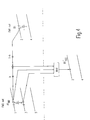
- FIG. 3 shows a schematic illustration above a broken line of two sub-images BO NR and A1 of the original image signal, as are read from the two sub-image memories 1 and 2 of the illustration according to FIG. 1.
- a field A1, oo is shown, which represents the first field of a sequence of the converted image signal. This signal of field A1, oo can be generated by the arrangement according to FIG. 1.
- the output signal of the first field memory 1 is used, from which the field A1 of the original image signal (with a doubled field frequency) is read out.
- the field BO of the original image signal has already been read into the field memory 2, but in a noise-reduced form. This signal is now on the output side at the same time as the Si Signal A1 is available as signal BO NR at the output of the second field memory.
- the first field A1, oo of the sequence is obtained from these two output signals of the field memories 1 and 2 in accordance with the schematic representation in FIG. 3.
- This partial image A1 100 to be generated has the correct position vertically and temporally in relation to the partial image A1 of the original image signal. It is therefore only necessary to apply a noise reduction, in particular a line flicker reduction is not necessary.
- the output signals of the field memories 1 and 2 are used for the noise reduction, it being advantageous for the field content of a motion compensation to be used for the field that was read out of the field memory 2 and that does not have the correct temporal position in relation to the field A1 100 to be generated to undergo.
- the motion vector determined by the arrangement 5 for motion compensation according to FIG. 1 is used. This motion vector is designated Vx in FIG. 3.
- the pixel from the sub-picture A1 is multiplied by a factor 1-k and the pixel from the sub-picture BO NR by a factor k. These two multiplied values are added together and form the value of the marked pixel of field A1 100 .
- k is chosen to be small, then little or no noise reduction should be undertaken and this pixel is essentially obtained from the corresponding pixel of sub-picture A1. With a larger factor k, the value of the pixel from the sub-picture BO NR is also increasingly used.
- the generated field A1 100 corresponds to the field A1 of the original image signal except for the noise reduction that has been carried out.
- ES is read into the second partial image memory 2 according to FIG. 1 and is available as Al NR for partial images to be subsequently generated therein.
- the multiplexer 8 is connected to its first input as shown in FIG. 1, since here the output signals of the noise reduction according to the schematic representation in FIG. 3 are used as the output signal and thus as a signal for the field A1 100 be used.
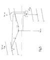
- Fig. 4 shows an illustration corresponding to Figure 3 but for the recovery of the second field B1 -. 100 of the sequence.
- This second field of the sequence has neither the vertical nor the correct position in relation to the two fields of the original image signal. Motion compensation and line flicker reduction are therefore carried out.
- field B1 of the original image signal is read from the first field memory and field A1 of the original image signal is read from the second field memory, but in a noise-reduced form.
- an image point of the image line 2 characterized - in the representation of Figure 4 is for the partial image B1.
- the value of this pixel is generated by median filtering from three values, as is obtained from the sub-images A1NR and B1.
- the first of these values is obtained from the image line 3 for the pixel which, after application of half the motion vector (v x ⁇ ) has the same position as the pixel to be generated in drawing B1-100.
- the second input signal of the median filter is obtained from the pixel of the same line position of line 1 of the field A1NR. The value of this pixel is also multiplied by a factor k.
- the one pixel of the image line 2 of the field B1 the same after application of the half negative motion vector (v x ⁇ t) image line position has, as to be generated pixel of the partial image B1 - 100, multiplied by a factor 1-k.
- These two values are added and the sum forms the third input signal for median filtering.
- the median filtering is used to select from these three input signals the one that has the mean instantaneous amplitude value. This signal is the value of the designated pixel of the second field B1 - 100 of the sequence.
- the multiplexer 8 is according to the representation of Figure 1 to generate the values of the partial image B1 -. 100 connected to its second input to which the output signal of the arrangement 7 to the line flicker reduction is supplied.
- FIG. 5 also shows a representation corresponding to FIGS. 3 and 4, but in the representation according to FIG. 5 the third field B1 * 100 of the sequence is to be generated.
- the two corresponding partial images A1 and B1 of the original image signal are in turn used to generate this partial image.
- the field B1 is read out from the field memory 1 of the illustration according to FIG. 1.
- the field A1 which has already been reduced in noise, is read from the field memory 2 in the illustration according to FIG. 1.
- a median filtering from three input signals is carried out for the generation of a pixel of the image line 3 of the partial image Bl * ioo marked in FIG. 5.
- the first of these input signals represents the value of the image point of image line 2 of field B1, which has the same image line position in its image line as the image point to be generated in its image line. Furthermore, from the field A1, as it is read from the second field memory , that pixel is used which, after correction by the motion vector Vx, has the same line position as the pixel to be generated. This motion-compensated pixel represents the second input signal of the median filter.
- the third input signal is formed from a sum in which on the one hand the value of the same line position of the pixel of the image line 4 of the field B1, which is multiplied by a factor 1-k, and the value of second input signal of the median filter, which is multiplied by a factor k. This sum represents the third input signal of the median filter and is simultaneously read in as an input signal in the second field memory, from which it can be read out again for field images to be generated subsequently.
- the multiplexer 8 of the block diagram according to FIG. 1 is switched to its second input for the generation of the third field BL * 100 of the sequence, since a line flicker reduction and also a movement compensation must be carried out.
- FIG. 6 shows a representation corresponding to FIGS. 3 to 5, the values of the fourth field B1 + , oo of the sequence having to be obtained in the representation according to FIG. 6.
- the sub-picture B1 used (in a reduced-noise form) of the original picture signal has the correct position vertically, ie has the same position as the picture B1 + , oo , a line flicker reduction is not necessary here.
- the sub-picture B1 NR does not have the correct position in time, so that motion compensation is required.
- the multiplexer 8 is switched to its third input as shown in FIG. 1.
- the type of generation of a sequence of the four partial images corresponding to FIGS. 3 to 6 is repeated continuously, four corresponding partial images of the converted image signal being obtained for every two output partial images of the original image signal.
Landscapes
- Engineering & Computer Science (AREA)
- Multimedia (AREA)
- Signal Processing (AREA)
- Picture Signal Circuits (AREA)
- Television Systems (AREA)
Applications Claiming Priority (2)
| Application Number | Priority Date | Filing Date | Title |
|---|---|---|---|
| DE4237225A DE4237225A1 (de) | 1992-11-04 | 1992-11-04 | Anordnung zur Verdopplung der Teilbildfrequenz eines Bildsignals |
| DE4237225 | 1992-11-04 |
Publications (2)
| Publication Number | Publication Date |
|---|---|
| EP0596561A1 true EP0596561A1 (fr) | 1994-05-11 |
| EP0596561B1 EP0596561B1 (fr) | 1998-01-07 |
Family
ID=6472082
Family Applications (1)
| Application Number | Title | Priority Date | Filing Date |
|---|---|---|---|
| EP93203010A Expired - Lifetime EP0596561B1 (fr) | 1992-11-04 | 1993-10-28 | Dispositif de doublement de la fréquence de trame d'un signal d'image |
Country Status (4)
| Country | Link |
|---|---|
| US (1) | US5469217A (fr) |
| EP (1) | EP0596561B1 (fr) |
| JP (1) | JPH06217264A (fr) |
| DE (2) | DE4237225A1 (fr) |
Families Citing this family (7)
| Publication number | Priority date | Publication date | Assignee | Title |
|---|---|---|---|---|
| EP1307056B1 (fr) * | 1995-06-30 | 2004-10-06 | Mitsubishi Denki Kabushiki Kaisha | Dispositif de conversion de balayage avec une résolution verticale améliorée et un dispositif de réduction du scintillement |
| US5844619A (en) * | 1996-06-21 | 1998-12-01 | Magma, Inc. | Flicker elimination system |
| US6014182A (en) | 1997-10-10 | 2000-01-11 | Faroudja Laboratories, Inc. | Film source video detection |
| US6108041A (en) * | 1997-10-10 | 2000-08-22 | Faroudja Laboratories, Inc. | High-definition television signal processing for transmitting and receiving a television signal in a manner compatible with the present system |
| KR100730499B1 (ko) * | 1999-04-23 | 2007-06-22 | 소니 가부시끼 가이샤 | 화상 변환 장치 및 방법 |
| US6330032B1 (en) * | 1999-09-30 | 2001-12-11 | Focus Enhancements, Inc. | Motion adaptive de-interlace filter |
| JP2006165974A (ja) * | 2004-12-07 | 2006-06-22 | Samsung Sdi Co Ltd | 映像信号処理回路、画像表示システム、及び、映像信号処理方法 |
Citations (1)
| Publication number | Priority date | Publication date | Assignee | Title |
|---|---|---|---|---|
| EP0502693A2 (fr) * | 1991-03-04 | 1992-09-09 | Sony Corporation | Récepteur de télévision pour système de télévision à définition améliorée |
Family Cites Families (3)
| Publication number | Priority date | Publication date | Assignee | Title |
|---|---|---|---|---|
| NL8402707A (nl) * | 1984-09-05 | 1986-04-01 | Philips Nv | Rasterfrequentieverdubbelingsschakeling. |
| GB8608876D0 (en) * | 1986-04-11 | 1986-05-14 | Rca Corp | Television display system |
| AU618411B2 (en) * | 1988-10-13 | 1991-12-19 | Sony Corporation | Flicker reduction apparatus |
-
1992
- 1992-11-04 DE DE4237225A patent/DE4237225A1/de not_active Withdrawn
-
1993
- 1993-10-28 DE DE59307932T patent/DE59307932D1/de not_active Expired - Fee Related
- 1993-10-28 US US08/146,287 patent/US5469217A/en not_active Expired - Fee Related
- 1993-10-28 EP EP93203010A patent/EP0596561B1/fr not_active Expired - Lifetime
- 1993-11-01 JP JP5273742A patent/JPH06217264A/ja active Pending
Patent Citations (1)
| Publication number | Priority date | Publication date | Assignee | Title |
|---|---|---|---|---|
| EP0502693A2 (fr) * | 1991-03-04 | 1992-09-09 | Sony Corporation | Récepteur de télévision pour système de télévision à définition améliorée |
Non-Patent Citations (2)
| Title |
|---|
| FILLIMAN ET AL.: "INTERLACE TO PROGRESSIVE SCAN CONVERTER FOR IDTV", IEEE TRANSACTIONS ON CONSUMER ELECTRONICS, vol. 38, no. 3, August 1992 (1992-08-01), NEW YORK US, pages 135 - 143 * |
| MIYAGUCHI ET AL.: "Digital TV with Serial Video Processor", IEEE 1990 INTERNATIONAL CONFERENCE ON CONSUMER ELECTRONICS, 6 June 1990 (1990-06-06), ROSEMONT, ILLINOIS, pages 324 - 325 * |
Also Published As
| Publication number | Publication date |
|---|---|
| DE59307932D1 (de) | 1998-02-12 |
| JPH06217264A (ja) | 1994-08-05 |
| US5469217A (en) | 1995-11-21 |
| DE4237225A1 (de) | 1994-05-05 |
| EP0596561B1 (fr) | 1998-01-07 |
Similar Documents
| Publication | Publication Date | Title |
|---|---|---|
| DE69123359T3 (de) | Videobildverarbeitung | |
| DE3609887C2 (de) | Schaltungsanordnung zur Erzeugung von Bemessungsfaktoren für ein rekursives Filter für Videosignale | |
| DE69422255T2 (de) | Verfahren und Vorrichtung zum bewegungsausgeglichenen Interpolieren von zwischenliegenden Halbbildern oder Bildern | |
| DE69405740T2 (de) | Verfahren und anordnung für bewegungskompensierende interpolation | |
| DE69126930T2 (de) | Video-Bewegungsvektorabschätzung mit asymmetrischem Aktualisierungsgebiet | |
| EP0472239A2 (fr) | Méthode d'évaluation des mouvements horizontaux dans le contenu d'images d'un signal de télévision | |
| EP0318757A2 (fr) | Récepteur de télévision avec un dispositif de suppression des perturbations de scintillement | |
| EP0445336A1 (fr) | Méthode et dispositif de réduction du scintillement du bord d'une image de télévision | |
| DE69830471T2 (de) | Interpolator mit einem gewichteten Medianfilter | |
| DE3330570A1 (de) | Doppelabtastender zeilensprungfreier fernsehempfaenger | |
| DE69009612T2 (de) | Verfahren zur Behandlung und zur Übertragung einer Folge von stereoskopischen Fernsehbilpaaren durch einen Kanal, der einen analogen und einen digitalen Weg enthält. | |
| EP0471878A1 (fr) | Procédé de superposition image-dans-image et appareil pour suivre ce procédé | |
| EP1125428B1 (fr) | Circuit permettant de transformer un debit binaire | |
| EP0596561B1 (fr) | Dispositif de doublement de la fréquence de trame d'un signal d'image | |
| EP0257129B1 (fr) | Procédé de reproduction de signaux de télévision avec une qualité d'image améliorée | |
| EP0554495B1 (fr) | Méthode et configuration de circuit pour la réduction du scintillement basée sur le vecteur de mouvement dans un récepteur de télévision | |
| EP0705031B1 (fr) | Procédé et circuit pour réduire le scintillement pour un dispositif de traitement signal vidéo | |
| EP0727904B1 (fr) | Méthode et arrangement de circuit pour la réduction de scintillation dans un dispositif de traitement de signal vidéo | |
| EP0739130B1 (fr) | Procédé et circuit d'insertion d'image dans l'image | |
| DE69215118T2 (de) | Nichtlinearer Signalprozessor | |
| EP0753972A2 (fr) | Procédé d'interpolation intertrame de signaux de différence de couleur et circuit pour la réalisation du procédé | |
| DE4414173C1 (de) | Verfahren zur Umsetzung einer Bildfolge von Halbbildern mit Zeilensprung auf eine Bildfolge von zeilensprungfreien Bildern und Schaltungsanordnung zur Durchführung des Verfahrens | |
| DE3909921A1 (de) | Verfahren und schaltungsanordnung zur wiedergabe von empfangenen videosignalen | |
| EP0941603B1 (fr) | Procede et configuration de circuit pour generer une serie d'images progressives | |
| DE69129871T2 (de) | Verfahren und Vorrichtung zur Signalverarbeitung |
Legal Events
| Date | Code | Title | Description |
|---|---|---|---|
| PUAI | Public reference made under article 153(3) epc to a published international application that has entered the european phase |
Free format text: ORIGINAL CODE: 0009012 |
|
| AK | Designated contracting states |
Kind code of ref document: A1 Designated state(s): DE FR GB |
|
| RAP1 | Party data changed (applicant data changed or rights of an application transferred) |
Owner name: N.V. PHILIPS' GLOEILAMPENFABRIEKEN Owner name: PHILIPS PATENTVERWALTUNG GMBH |
|
| 17P | Request for examination filed |
Effective date: 19941019 |
|
| GRAG | Despatch of communication of intention to grant |
Free format text: ORIGINAL CODE: EPIDOS AGRA |
|
| 17Q | First examination report despatched |
Effective date: 19970204 |
|
| GRAH | Despatch of communication of intention to grant a patent |
Free format text: ORIGINAL CODE: EPIDOS IGRA |
|
| GRAH | Despatch of communication of intention to grant a patent |
Free format text: ORIGINAL CODE: EPIDOS IGRA |
|
| GRAA | (expected) grant |
Free format text: ORIGINAL CODE: 0009210 |
|
| AK | Designated contracting states |
Kind code of ref document: B1 Designated state(s): DE FR GB |
|
| REF | Corresponds to: |
Ref document number: 59307932 Country of ref document: DE Date of ref document: 19980212 |
|
| GBT | Gb: translation of ep patent filed (gb section 77(6)(a)/1977) |
Effective date: 19980205 |
|
| ET | Fr: translation filed | ||
| RAP4 | Party data changed (patent owner data changed or rights of a patent transferred) |
Owner name: KONINKLIJKE PHILIPS ELECTRONICS N.V. Owner name: PHILIPS PATENTVERWALTUNG GMBH |
|
| REG | Reference to a national code |
Ref country code: FR Ref legal event code: CD |
|
| PLBE | No opposition filed within time limit |
Free format text: ORIGINAL CODE: 0009261 |
|
| STAA | Information on the status of an ep patent application or granted ep patent |
Free format text: STATUS: NO OPPOSITION FILED WITHIN TIME LIMIT |
|
| 26N | No opposition filed | ||
| PGFP | Annual fee paid to national office [announced via postgrant information from national office to epo] |
Ref country code: GB Payment date: 19991021 Year of fee payment: 7 |
|
| PGFP | Annual fee paid to national office [announced via postgrant information from national office to epo] |
Ref country code: FR Payment date: 19991026 Year of fee payment: 7 |
|
| PGFP | Annual fee paid to national office [announced via postgrant information from national office to epo] |
Ref country code: DE Payment date: 19991215 Year of fee payment: 7 |
|
| PG25 | Lapsed in a contracting state [announced via postgrant information from national office to epo] |
Ref country code: GB Free format text: LAPSE BECAUSE OF NON-PAYMENT OF DUE FEES Effective date: 20001028 |
|
| GBPC | Gb: european patent ceased through non-payment of renewal fee |
Effective date: 20001028 |
|
| PG25 | Lapsed in a contracting state [announced via postgrant information from national office to epo] |
Ref country code: FR Free format text: LAPSE BECAUSE OF NON-PAYMENT OF DUE FEES Effective date: 20010629 |
|
| PG25 | Lapsed in a contracting state [announced via postgrant information from national office to epo] |
Ref country code: DE Free format text: LAPSE BECAUSE OF NON-PAYMENT OF DUE FEES Effective date: 20010703 |
|
| REG | Reference to a national code |
Ref country code: FR Ref legal event code: ST |