EP0592064A2 - Field effect transistor and method of production - Google Patents
Field effect transistor and method of production Download PDFInfo
- Publication number
- EP0592064A2 EP0592064A2 EP93302706A EP93302706A EP0592064A2 EP 0592064 A2 EP0592064 A2 EP 0592064A2 EP 93302706 A EP93302706 A EP 93302706A EP 93302706 A EP93302706 A EP 93302706A EP 0592064 A2 EP0592064 A2 EP 0592064A2
- Authority
- EP
- European Patent Office
- Prior art keywords
- insulating film
- aperture
- resist pattern
- semiconductor epitaxial
- metal
- Prior art date
- Legal status (The legal status is an assumption and is not a legal conclusion. Google has not performed a legal analysis and makes no representation as to the accuracy of the status listed.)
- Granted
Links
Images



Classifications
-
- H—ELECTRICITY
- H10—SEMICONDUCTOR DEVICES; ELECTRIC SOLID-STATE DEVICES NOT OTHERWISE PROVIDED FOR
- H10D—INORGANIC ELECTRIC SEMICONDUCTOR DEVICES
- H10D30/00—Field-effect transistors [FET]
- H10D30/01—Manufacture or treatment
- H10D30/015—Manufacture or treatment of FETs having heterojunction interface channels or heterojunction gate electrodes, e.g. HEMT
-
- H—ELECTRICITY
- H10—SEMICONDUCTOR DEVICES; ELECTRIC SOLID-STATE DEVICES NOT OTHERWISE PROVIDED FOR
- H10D—INORGANIC ELECTRIC SEMICONDUCTOR DEVICES
- H10D64/00—Electrodes of devices having potential barriers
- H10D64/01—Manufacture or treatment
- H10D64/012—Manufacture or treatment of electrodes comprising a Schottky barrier to a semiconductor
- H10D64/0124—Manufacture or treatment of electrodes comprising a Schottky barrier to a semiconductor to Group III-V semiconductors
- H10D64/0125—Manufacture or treatment of electrodes comprising a Schottky barrier to a semiconductor to Group III-V semiconductors characterised by the sectional shape, e.g. T or inverted T
-
- H—ELECTRICITY
- H10—SEMICONDUCTOR DEVICES; ELECTRIC SOLID-STATE DEVICES NOT OTHERWISE PROVIDED FOR
- H10D—INORGANIC ELECTRIC SEMICONDUCTOR DEVICES
- H10D64/00—Electrodes of devices having potential barriers
- H10D64/20—Electrodes characterised by their shapes, relative sizes or dispositions
- H10D64/27—Electrodes not carrying the current to be rectified, amplified, oscillated or switched, e.g. gates
- H10D64/311—Gate electrodes for field-effect devices
- H10D64/411—Gate electrodes for field-effect devices for FETs
-
- Y—GENERAL TAGGING OF NEW TECHNOLOGICAL DEVELOPMENTS; GENERAL TAGGING OF CROSS-SECTIONAL TECHNOLOGIES SPANNING OVER SEVERAL SECTIONS OF THE IPC; TECHNICAL SUBJECTS COVERED BY FORMER USPC CROSS-REFERENCE ART COLLECTIONS [XRACs] AND DIGESTS
- Y10—TECHNICAL SUBJECTS COVERED BY FORMER USPC
- Y10S—TECHNICAL SUBJECTS COVERED BY FORMER USPC CROSS-REFERENCE ART COLLECTIONS [XRACs] AND DIGESTS
- Y10S148/00—Metal treatment
- Y10S148/10—Lift-off masking
-
- Y—GENERAL TAGGING OF NEW TECHNOLOGICAL DEVELOPMENTS; GENERAL TAGGING OF CROSS-SECTIONAL TECHNOLOGIES SPANNING OVER SEVERAL SECTIONS OF THE IPC; TECHNICAL SUBJECTS COVERED BY FORMER USPC CROSS-REFERENCE ART COLLECTIONS [XRACs] AND DIGESTS
- Y10—TECHNICAL SUBJECTS COVERED BY FORMER USPC
- Y10S—TECHNICAL SUBJECTS COVERED BY FORMER USPC CROSS-REFERENCE ART COLLECTIONS [XRACs] AND DIGESTS
- Y10S148/00—Metal treatment
- Y10S148/139—Schottky barrier
-
- Y—GENERAL TAGGING OF NEW TECHNOLOGICAL DEVELOPMENTS; GENERAL TAGGING OF CROSS-SECTIONAL TECHNOLOGIES SPANNING OVER SEVERAL SECTIONS OF THE IPC; TECHNICAL SUBJECTS COVERED BY FORMER USPC CROSS-REFERENCE ART COLLECTIONS [XRACs] AND DIGESTS
- Y10—TECHNICAL SUBJECTS COVERED BY FORMER USPC
- Y10S—TECHNICAL SUBJECTS COVERED BY FORMER USPC CROSS-REFERENCE ART COLLECTIONS [XRACs] AND DIGESTS
- Y10S438/00—Semiconductor device manufacturing: process
- Y10S438/942—Masking
- Y10S438/948—Radiation resist
- Y10S438/951—Lift-off
Definitions
- the present invention relates to a field effect transistor having a T-shaped gate electrode and a method for producing the field effect transistor.
- Figures 4(a) to 4(k) are cross-sectional views illustrating process steps in a method for fabricating a prior art HEMT (High Electron Mobility Transistor) disclosed in, for example, Japanese Published Patent Application No. 63-174374 and Electronics Letters 24, 1988, p.1327.
- HEMT High Electron Mobility Transistor
- a GaAs buffer layer 21, an intrinsic type (hereinafter referred to as i type) GaAs layer 22, an n type AIGaAs layer 23, and an n + type GaAs layer 24 are successively grown on a semi-insulating GaAs substrate (not shown) by epitaxial growth.
- an Si0 2 film is deposited on the substrate to a thickness of about 3000 angstroms, forming a first insulating film 25.
- a resist pattern 27 having an aperture of 0.5 micron width is formed on the first insulating film 25 (figure 4(a)).
- the first insulating film 25 is etched using the first resist pattern 27 as a mask to form a first aperture 25a.
- the first insulating film 25 is etched by dry etching using a mixture gas of CHF 3 and 0 2 or CF 4 and 0 2 .
- the n + type GaAs layer 24 is etched to form a recess 24a having a depth of about 1000 angstroms.
- the GaAs layer 24 is etched by reactive ion etching using CCI 2 F 2 or by wet etching using a mixture of tartaric acid and hydrogen peroxide solution as an etchant (figure 4(c)).
- the n + type GaAs layer 24 is etched to expose the surface of the n type AIGaAs layer 23, the etching may be stopped in the n + type GaAs layer 24.
- an Si0 2 film is deposited on the n type AIGaAs layer 23 and the first insulating film 25 to a thickness of about 3000 angstroms, forming a second insulating film 28 (figure 4(e)).
- the Si0 2 film is deposited by plasma CVD.
- the second insulating film 28 is etched in the perpendicular direction to the surface of the substrate by sputter etching or reactive ion etching, leaving portions at opposite sides of the first aperture 25a to form a second aperture 28a.
- a width W1 of the n type AIGaAs layer 23 exposed at the bottom of the second aperture 28a is about 0.25 micron.
- a refractory metal 29, such as WSi is deposited on the substrate to a thickness of 1500 angstroms by sputtering, followed by annealing.
- a low resistance metal layer 30 comprising Ti 500 angstroms thick, Pt 1000 angstroms thick, and Au 3000 angstroms thick is formed on the refractory metal layer 29 by sputtering.
- a resist pattern 31 is formed on the low resistance metal layer 30.
- the low resistance metal layer 30 comprising Ti/Pt/Au is patterned by ion milling, and the refractory metal layer 29 comprising WSi and the insulating film 25 comprising Si0 2 are patterned by reactive ion etching (figure 4(h)).
- the refractory metal layer 29 and the insulating film 25 are excessively etched, so that the width of the refractory metal layer 29 is narrower than the width of the low resistance metal layer 30.
- Figure 4(i) illustrates a case where the etching rate of the reactive ion etching is further increased. In this case, the width of the refractory metal layer 29 is further decreased and the insulating film 25 is completely removed.
- a resist pattern for forming ohmic electrodes (not shown) is formed on the substrate, followed by a deposition of an ohmic electrode metal 32 comprising AuGe/Ni/Au and lift-off, resulting in a T-shaped gate electrode 33 and ohmic electrodes, i.e., source and drain electrodes 32a and 32b. Thereafter, the substrate is annealed at 400 C for two minutes to complete the HEMT of figure 4(k).
- the gate-to-source capacitance (Cgs) is reduced.
- the insulating film 28 remaining on opposite sides of the lower part of the T-shaped gate electrode 33 protects the surface of the n type AIGaAs layer 23.
- a crystal region in which electrons travel i.e., a region of the i type GaAs layer 22 where a two-dimensional electron gas is formed, is spaced apart from a crystal region that supplies electrons, i.e., the n type Al-GaAs layer 23, by the heterojunction to prevent the electrons from being scattered by donor impurities, whereby the electron mobility of the transistor is increased.
- the second insulating film 28 is deposited on the substrate to fill the first aperture 25a and then etched away leaving portions on opposite side walls of the aperture 25a, which portions form a second aperture 28a having a width W1 of 0.25 micron that would be a gate length. Thereafter, the refractory metal 29 is deposited in the aperture 28a to form the lower part of the gate electrode.
- the first insulating film 25 is also etched and the thickness thereof is reduced, whereby, in the structure of figure 4(k), the interval between the overhanging part 33a of the T-shaped gate electrode 33 and the surface of the n + type GaAs layer 24 whereon the source and drain electrodes 32a and 33b are present is reduced, resulting in an increase in the gate-to-source capacitance.
- the above-described problem can be solved by increasing the thickness of the first insulating film 25, if the thickness of the first insulating film 25 increases, the etching precision when the aperture 25a is formed in the first insulating film 25 is reduced, and the aperture 25a is not completely filled with the second insulating film 28 when the insulating film 28 is deposited on the substrate. In this case, it is difficult to form the fine aperture 28a having a width W1 of about 0.25 micron with high controllability.
- the width W1 of the aperture 28a at the n type AIGaAs layer 23 varies according to the thickness of the second insulating film 28 deposited in the step of figure 4(e). More specifically, the width W1 decreases with an increase in the thickness of the second insulating film 28. When the second insulating film 28 is deposited to 3000 angstroms as described above, the width W1 is about 0.25 micron. If the thickness of the second insulating film 28 is further increased to further reduce the gate length, the width of the V-shaped aperture 28a decreases.
- the angle of the V-shaped groove 29a formed opposite the V-shaped aperture 28a gradually decreases and the refractory metal 29 is not evenly deposited on the surface of the groove 29a.
- a cavity 30a is formed in the low resistance metal layer 30 deposited on the refractory metal layer 29, which cavity increases the gate resistance.
- Japanese Published Patent Application No. 63-204772 proposes an improved method of forming a T-shaped gate structure, in which an upper metal layer of the T-shaped gate electrode is formed by a plating method using a lower metal layer of the gate electrode as a feeding electrode.
- this plating method it is difficult to apply ions onto the uneven surface, such as the surface with the V-shaped groove 29a, with keeping the ion concentration constant, so that it is impossible to grow the upper metal layer with no cavity.
- a method of producing a field effect transistor includes depositing a first insulating film and a refractory metal film on a semiconductor epitaxial substrate, forming a first aperture penetrating the first insulating film and the metal thin film, which aperture provides a gate electrode production region, forming a second insulating film on the refractory metal film, etching the second insulating film in a direction perpendicular to the surface of the substrate leaving portions on opposite side walls of the first aperture to form a second aperture, which second aperture provides a gate length, depositing a gate metal on the whole surface of the substrate, and patterning the gate metal layer, the first insulating film, and the refractory metal film in a prescribed width to form a T-shaped gate structure.
- the first insulating film is not etched and its thickness remains as it is deposited, whereby the space between the over-hanging portion of the T-shaped gate electrode and the source (drain) electrode is increased.
- the first and second insulating films are completely removed and a third insulating film thinner than 500 angstroms is deposited on the whole surface of the T-shaped gate electrode and the substrate. Therefore, the insulating film under the overhanging portion of the T-shaped gate electrode is reduced. In addition, the third insulating film protects the active region of the device.
- a first metal is deposited on the substrate to fill the second aperture, and a second metal is applied onto the first metal layer by pulse plating or electroless plating using the first metal layer as a feeding electrode. Therefore, even if the surface of the first metal layer is uneven, the second metal layer is favorably grown on the first metal layer with no cavity in the second metal layer.
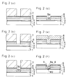
- Figure 1 is a cross-sectional view illustrating a HEMT in accordance with a first embodiment of the present invention.
- Figures 2(a) to 2(1) are cross-sectional views illustrating process steps in a method of producing the HEMT of figure 1.
- reference numeral 1 designates a GaAs buffer layer.
- An i type GaAs layer 2 is disposed on the buffer layer 1.
- An n type AIGaAs layer 3 is disposed on the GaAs layer 2.
- An n + type GaAs layer 4 is disposed on the AIGaAs layer 3.
- a recess 4a penetrates through a portion of the GaAs layer 4.
- a T-shaped gate electrode 15a is disposed on the n type AIGaAs layer 3 exposed at the bottom of the recess 4a.
- the T-shaped gate electrode 15a comprises a refractory metal layer 9, a low resistance metal layer 10, and a metal layer 13 for ohmic electrodes.
- the ohmic electrodes i.e., source and drain electrodes 13a and 13b, are disposed on the GaAs layer 4 spaced apart from each other.
- the whole surface of this HEMT is covered with an insulating film 12 except for the metal layer 13.
- Reference numeral 14 designates a feeding metal layer.
- FIG. 2(a) there are successively grown on a semi-insulating GaAs substrate (not shown) by epitaxial growth, the GaAs buffer layer 1, the i type GaAs layer 2, the n type AIGaAs layer 3, and the n + type GaAs layer 4.
- Si0 2 is deposited on the substrate to a thickness of about 3000 angstroms by plasma CVD to form a first insulating film 5.
- WSi is deposited on the first insulating film 5 to a thickness of about 500 angstroms by sputtering to form a refractory metal thin film 6, and a resist pattern 7 having an aperture of 0.5 micron is formed on the refractory metal thin film 6.
- the refractory metal thin film 6 is etched by dry etching using SF 6 and the insulating film 5 is etched by dry etching using CHF 3 , CF 4 , or the like, forming a first aperture 5a.
- the n + GaAs layer 4 is etched by reactive ion etching using CC1 2 F 2 , C1 2 , or SiCl 4 , or wet etching using a mixture of tartaric acid and hydrogen peroxide solution as an etchant, forming a recess 4a having a depth of about 1000 angstroms (figure 2(c)).
- the n + type GaAs layer 4 is etched to expose the surface of the n type AIGaAs layer 3, the etching may be stopped in the n + type GaAs layer 4.
- Si0 2 is deposited over the surface of the substrate to a thickness of 3000 to 5000 angstroms by plasma CVD, forming a second insulating film 8.
- the second insulating film 8 is etched in the vertical direction to the surface of the substrate by sputter etching or reactive ion etching, leaving portions on the opposite side walls of the first aperture 5a.
- the refractory WSi thin film 6 serves as an etching stopper layer, the thickness of the first insulating film 5 lying under the WSi thin film 6 is not reduced.
- the etching rate of a mixture gas of CHF 3 and 0 2 to Si0 2 is about 500 angstroms/min, the etching rate of the gas to WSi is only 100 angstroms/min.
- a time interval required for etching the second insulating film 8 comprising Si0 2 5000 angstroms thick is 10 min
- a time interval required for etching the WSi thin film 6 500 angstroms thick is 5 min and, therefore, the first insulating film 5 is not etched even if the second insulating film 8 is excessively etched by 50 percent.
- the width w 2 of the second aperture 8a which is equivalent to a gate length, varies according to the thickness of the second insulating film 8 deposited in the step of figure 2(e). For example, when the thickness of the second insulating film 8 increases from 3000 angstroms to 5000 angstroms, the width w 2 decreases from 0.25 micron to 0.15 micron.
- a refractory metal such as WSi
- a refractory metal layer 9 is deposited on the whole surface of the substrate to a thickness of about 1500 angstroms by sputtering, resulting in a refractory metal layer 9.
- the substrate is annealed at 400 to 500 °C to remove damages on the surface of the aperture 8a due to the sputtering.
- Au or the like is deposited on the refractory metal layer 9 to a thickness of about 500 angstroms, forming a feeding metal layer 14 which serves as a feeding electrode when a metal layer is plated thereon.
- Au or the like is applied onto the feeding metal layer 14 to a thickness of about 4000 angstroms by pulse plating or electroless plating, forming a low resistance metal layer 10.
- the pulse plating and the electroless plating employed for growing the low resistance metal layer 10 have the following advantages.
- the width w 2 of the aperture 8a is narrower than 0.2 micron
- the width of the V-shaped groove 9a formed on the surface of the refractory metal layer 9 during depositing the metal layer 9 by sputtering is very narrow.
- the feeding metal layer 14 is present on the surface of the V-shaped groove 9a, when the low resistance metal layer 10 comprising Au is grown on the feeding metal layer 14, Au ions are evenly applied to the surface of the feeding metal layer 14 in the V-shaped groove 9, resulting in no cavity in the low resistance metal layer 10.
- a resist pattern 11 having a prescribed width is formed on the low resistance metal layer 10. Then, using the resist pattern 11 as a mask, the low resistance metal layer 10 and the feeding metal layer 14 are etched by ion milling, and the WSi refractory metal layer 9, the WSi refractory metal thin film 6, and the first insulating film 5 are etched by reactive ion etching. During the etching, the refractory metal layers 9 and 6 and the insulating film 5 are excessively etched.
- Si0 2 is deposited on the whole surface of the structure to a thickness of 500 angstroms or less by plasma CVD, forming a third insulating film 12.
- a resist pattern (not shown) as a mask, portions of the third insulating film 12 on the top of the T-shaped gate structure 15 and on regions of the n + type GaAs layer 4 where source and drain electrodes are to be disposed are removed by reactive ion etching, followed by a deposition of an ohmic electrode metal 13 and lift-off, resulting in a T-shaped gate electrode 15a and ohmic electrodes, i.e., source and drain electrodes 13a and 13b (figure 2(1)).
- the substrate is annealed at 400 ° C for a few minutes to complete the HEMT of figure 1.
- the third insulating film 12 is formed in the step of figure 2(k), since the material, i.e., Si0 2 , is not sufficiently applied to the over-hanging portions 15b of the T-shaped gate structure 15, the thickness of the insulating film 12 on the over- hanging portions is very thin.
- the Au layer 14 is formed on the refractory metal layer 9
- a Ti film may be formed in place of the refractory metal layer 9 and then the Au layer 14 is deposited to a thickness of 2000 angstroms.
- the thickness of the first insulating film 5 deposited in the step of figure 2-(a) is 2000 angstroms
- the thickness of the first insulating film 25 etched in the step of figure 4(f) is 1000 angstroms.
- the interval between the over-hanging portion 15b of the T-shaped gate structure 15a and the n + type GaAs layer 4 of the HEMT of figure 1 is 1000 angstroms longer than that of the prior art HEMT because of the increase in the thickness of the insulating film 5, whereby the capacitance beneath the over-hanging portion 15b is reduced to half of that of the prior art HEMT, resulting in a reduction in the gate-to-source capacitance.
- portions of the second insulating film 28 remain on opposite sides of the lower part of the T-shaped gate structure 33.
- the insulating film 12 as thin as or thinner than 500 angstroms is present under the T-shaped gate structure 15a, so that the dielectric constant between the over-hanging portion 15b and the n + type GaAs layer 4 is reduced as compared with that of the prior art HEMT, resulting in a further reduction in the gate-to-source capacitance Cgs.
- a high-performance HEMT with short gate length, reduced gate-to-source capacitance, and reduced gate resistance is achieved.
- Figures 3(a) and 3(b) are cross-sectional views illustrating process steps in a method of producing a HEMT according to a second embodiment of the present invention.
- the same reference numerals as in figures 2(a)-2(1) designate the same parts.
- a resist pattern 16 having an aperture of prescribed width is formed on the feeding metal layer 14 and then the low resistance metal layer 10 is grown on the feeding metal layer 14 by pulse plating or electroless plating (figure 3(a)).
- the feeding metal layer 14, the refractory metal layers 6 and 9, and the first insulating film 5 are patterned to form the T-shaped gate structure 15.
- the first and second insulating films 5 and 8 are removed in the same manner as described in the first embodiment, followed by the deposition of the third insulating film 12 and the formation of the source and drain electrodes 13a and 13b. Also in this second embodiment, a high-performance HEMT with short gate length, reduced gate-to-source capacitance, and reduced gate resistance is achieved.
- the GaAs heterojunction epitaxial substrate comprising the GaAs buffer, the i type GaAs, the n type AIGaAs, and the n + GaAs
- a GaAs heterojunction epitaxial substrate for a pseudomorphic HEMT including an i type InGaAs between the i type GaAs and the n type AIGaAs may be employed.
- the epitaxial substrate may comprises other semiconductor materials, such as InP.
- HEMTs While in the above-described embodiments HEMTs are employed, the present invention may be applied to other field effect transistors.
Landscapes
- Junction Field-Effect Transistors (AREA)
Abstract
Description
- The present invention relates to a field effect transistor having a T-shaped gate electrode and a method for producing the field effect transistor.
- Figures 4(a) to 4(k) are cross-sectional views illustrating process steps in a method for fabricating a prior art HEMT (High Electron Mobility Transistor) disclosed in, for example, Japanese Published Patent Application No. 63-174374 and Electronics
Letters 24, 1988, p.1327. - Initially, a
GaAs buffer layer 21, an intrinsic type (hereinafter referred to as i type)GaAs layer 22, an ntype AIGaAs layer 23, and an n+type GaAs layer 24 are successively grown on a semi-insulating GaAs substrate (not shown) by epitaxial growth. Then, an Si02 film is deposited on the substrate to a thickness of about 3000 angstroms, forming a firstinsulating film 25. Then, aresist pattern 27 having an aperture of 0.5 micron width is formed on the first insulating film 25 (figure 4(a)). - Then, as illustrated in figure 4(b), the first
insulating film 25 is etched using thefirst resist pattern 27 as a mask to form afirst aperture 25a. Preferably, the firstinsulating film 25 is etched by dry etching using a mixture gas of CHF3 and 02 or CF4 and 02. Then, using theresist pattern 27 and the firstinsulating film 25 as a mask, the n+type GaAs layer 24 is etched to form a recess 24a having a depth of about 1000 angstroms. Preferably, the GaAslayer 24 is etched by reactive ion etching using CCI2 F2 or by wet etching using a mixture of tartaric acid and hydrogen peroxide solution as an etchant (figure 4(c)). In figure 4(c), although the n+type GaAs layer 24 is etched to expose the surface of the ntype AIGaAs layer 23, the etching may be stopped in the n+type GaAs layer 24. - After removing the
resist pattern 27 using 02 ash or organic solvent as shown in figure 4(d), an Si02 film is deposited on the ntype AIGaAs layer 23 and the firstinsulating film 25 to a thickness of about 3000 angstroms, forming a second insulating film 28 (figure 4(e)). Preferably, the Si02 film is deposited by plasma CVD. - Then, as illustrated in figure 4(f), the second
insulating film 28 is etched in the perpendicular direction to the surface of the substrate by sputter etching or reactive ion etching, leaving portions at opposite sides of thefirst aperture 25a to form asecond aperture 28a. A width W1 of the ntype AIGaAs layer 23 exposed at the bottom of thesecond aperture 28a is about 0.25 micron. - Then, as illustrated in figure 4(g), a
refractory metal 29, such as WSi, is deposited on the substrate to a thickness of 1500 angstroms by sputtering, followed by annealing. Then, a lowresistance metal layer 30 comprising Ti 500 angstroms thick, Pt 1000 angstroms thick, and Au 3000 angstroms thick is formed on therefractory metal layer 29 by sputtering. - Then, a
resist pattern 31 is formed on the lowresistance metal layer 30. Using theresist pattern 31 as a mask, the lowresistance metal layer 30 comprising Ti/Pt/Au is patterned by ion milling, and therefractory metal layer 29 comprising WSi and theinsulating film 25 comprising Si02 are patterned by reactive ion etching (figure 4(h)). During the etching process, therefractory metal layer 29 and theinsulating film 25 are excessively etched, so that the width of therefractory metal layer 29 is narrower than the width of the lowresistance metal layer 30. Figure 4(i) illustrates a case where the etching rate of the reactive ion etching is further increased. In this case, the width of therefractory metal layer 29 is further decreased and theinsulating film 25 is completely removed. - After removing the
resist pattern 31 as shown in figure 4(j), a resist pattern for forming ohmic electrodes (not shown) is formed on the substrate, followed by a deposition of anohmic electrode metal 32 comprising AuGe/Ni/Au and lift-off, resulting in a T-shaped gate electrode 33 and ohmic electrodes, i.e., source anddrain electrodes - Since the
insulating film 25 comprising Si02 lying under therefractory metal layer 29 is completely removed in the step of figure 4(i), the gate-to-source capacitance (Cgs) is reduced. Theinsulating film 28 remaining on opposite sides of the lower part of the T-shaped gate electrode 33 protects the surface of the ntype AIGaAs layer 23. - In the conventional HEMT, a crystal region in which electrons travel, i.e., a region of the i
type GaAs layer 22 where a two-dimensional electron gas is formed, is spaced apart from a crystal region that supplies electrons, i.e., the n type Al-GaAs layer 23, by the heterojunction to prevent the electrons from being scattered by donor impurities, whereby the electron mobility of the transistor is increased. In the HEMT, in order to increase the cut-off frequency (ft), the maximum oscillation frequency (fmax), and the uni lateral gain (U) and reduce the noise factor (Fo), it is necessary to reduce the gate length (Lg), the source resistance (Rs), the gate-to-source capacitance (Cgs), and the gate resistance (Rg). - In the conventional method for producing the HEMT illustrated in figures 4(a)-4(k), since the gate electrode and the source and drain electrodes are formed self-alignedly, it is possible to reduce the gate length and the source resistance. In addition, since the gate electrode is formed in a T shape, the gate resistance is reduced to some extent.
- In the steps of figures 4(e) and 4(f), the second
insulating film 28 is deposited on the substrate to fill thefirst aperture 25a and then etched away leaving portions on opposite side walls of theaperture 25a, which portions form asecond aperture 28a having a width W1 of 0.25 micron that would be a gate length. Thereafter, therefractory metal 29 is deposited in theaperture 28a to form the lower part of the gate electrode. However, during etching the secondinsulating film 28, the firstinsulating film 25 is also etched and the thickness thereof is reduced, whereby, in the structure of figure 4(k), the interval between the overhangingpart 33a of the T-shaped gate electrode 33 and the surface of the n+type GaAs layer 24 whereon the source anddrain electrodes 32a and 33b are present is reduced, resulting in an increase in the gate-to-source capacitance. - Although it is thought that the above-described problem can be solved by increasing the thickness of the first
insulating film 25, if the thickness of the firstinsulating film 25 increases, the etching precision when theaperture 25a is formed in the firstinsulating film 25 is reduced, and theaperture 25a is not completely filled with the secondinsulating film 28 when theinsulating film 28 is deposited on the substrate. In this case, it is difficult to form thefine aperture 28a having a width W1 of about 0.25 micron with high controllability. - In the step of figure 4(f), the width W1 of the
aperture 28a at the ntype AIGaAs layer 23 varies according to the thickness of the secondinsulating film 28 deposited in the step of figure 4(e). More specifically, the width W1 decreases with an increase in the thickness of the secondinsulating film 28. When the secondinsulating film 28 is deposited to 3000 angstroms as described above, the width W1 is about 0.25 micron. If the thickness of the secondinsulating film 28 is further increased to further reduce the gate length, the width of the V-shaped aperture 28a decreases. When therefractory metal 29 is deposited in the narrow V-shaped aperture 28a, the angle of the V-shaped groove 29a formed opposite the V-shaped aperture 28a gradually decreases and therefractory metal 29 is not evenly deposited on the surface of thegroove 29a. As a result, acavity 30a is formed in the lowresistance metal layer 30 deposited on therefractory metal layer 29, which cavity increases the gate resistance. - Meanwhile, Japanese Published Patent Application No. 63-204772 proposes an improved method of forming a T-shaped gate structure, in which an upper metal layer of the T-shaped gate electrode is formed by a plating method using a lower metal layer of the gate electrode as a feeding electrode. In this plating method, however, it is difficult to apply ions onto the uneven surface, such as the surface with the V-
shaped groove 29a, with keeping the ion concentration constant, so that it is impossible to grow the upper metal layer with no cavity. - It is an object of the present invention to provide a method of producing a field effect transistor having a T-shaped gate structure with reduced gate-to-source capacitance.
- It is another object of the present invention to provide a method of producing a field effect transistor that reduces a gate length to reduce the gate resistance.
- It is still another object of the present invention to provide a method of producing a field effect transistor having a T-shaped gate structure with a gate length of 0.25 micron or less and no cavity in an upper metal layer thereof.
- Other objects and advantages of the present invention will become apparent from the detailed description given hereinafter; it should be understood, however, that the detailed description and specific embodiment are given by way of illustration only, since various changes and modifications within the spirit and scope of the invention will become apparent to those skilled in the art from this detailed description.
- According to a first aspect of the present invention, a method of producing a field effect transistor includes depositing a first insulating film and a refractory metal film on a semiconductor epitaxial substrate, forming a first aperture penetrating the first insulating film and the metal thin film, which aperture provides a gate electrode production region, forming a second insulating film on the refractory metal film, etching the second insulating film in a direction perpendicular to the surface of the substrate leaving portions on opposite side walls of the first aperture to form a second aperture, which second aperture provides a gate length, depositing a gate metal on the whole surface of the substrate, and patterning the gate metal layer, the first insulating film, and the refractory metal film in a prescribed width to form a T-shaped gate structure. During etching the second insulating film, since the refractory metal film serves as an etching stopper layer, the first insulating film is not etched and its thickness remains as it is deposited, whereby the space between the over-hanging portion of the T-shaped gate electrode and the source (drain) electrode is increased.
- According to a second aspect of the present invention, after producing the T-shaped gate electrode, the first and second insulating films are completely removed and a third insulating film thinner than 500 angstroms is deposited on the whole surface of the T-shaped gate electrode and the substrate. Therefore, the insulating film under the overhanging portion of the T-shaped gate electrode is reduced. In addition, the third insulating film protects the active region of the device.
- According to a third aspect of the present invention, after forming the second insulating film pattern with the second aperture that provides a gate length, a first metal is deposited on the substrate to fill the second aperture, and a second metal is applied onto the first metal layer by pulse plating or electroless plating using the first metal layer as a feeding electrode. Therefore, even if the surface of the first metal layer is uneven, the second metal layer is favorably grown on the first metal layer with no cavity in the second metal layer.
-
- Figure 1 is a cross-sectional view illustrating a HEMT in accordance with a first embodiment of the present invention;
- Figures 2(a) to 2(1) are cross-sectional views illustrating process steps in a method of producing the HEMT of figure 1;
- Figures 3(a) and 3(b) are cross-sectional views illustrating process steps in a method of producing a HEMT in accordance with a second embodiment of the present invention;
- Figures 4(a) to 4(k) are cross-sectional views illustrating process steps in a method of producing a HEMT according to the prior art; and
- Figure 5 s a cross-sectional view for explaining a problem in the method according to the prior art.
- Figure 1 is a cross-sectional view illustrating a HEMT in accordance with a first embodiment of the present invention. Figures 2(a) to 2(1) are cross-sectional views illustrating process steps in a method of producing the HEMT of figure 1.
- In figure 1,
reference numeral 1 designates a GaAs buffer layer. An i typeGaAs layer 2 is disposed on thebuffer layer 1. An ntype AIGaAs layer 3 is disposed on theGaAs layer 2. An n+type GaAs layer 4 is disposed on theAIGaAs layer 3. Arecess 4a penetrates through a portion of theGaAs layer 4. A T-shaped gate electrode 15a is disposed on the ntype AIGaAs layer 3 exposed at the bottom of therecess 4a. The T-shaped gate electrode 15a comprises arefractory metal layer 9, a lowresistance metal layer 10, and ametal layer 13 for ohmic electrodes. The ohmic electrodes, i.e., source anddrain electrodes GaAs layer 4 spaced apart from each other. The whole surface of this HEMT is covered with an insulatingfilm 12 except for themetal layer 13.Reference numeral 14 designates a feeding metal layer. - A description is give of the production method.
- Initially, as illustrated in figure 2(a), there are successively grown on a semi-insulating GaAs substrate (not shown) by epitaxial growth, the
GaAs buffer layer 1, the itype GaAs layer 2, the ntype AIGaAs layer 3, and the n+type GaAs layer 4. Then, Si02 is deposited on the substrate to a thickness of about 3000 angstroms by plasma CVD to form a firstinsulating film 5. Then, WSi is deposited on the first insulatingfilm 5 to a thickness of about 500 angstroms by sputtering to form a refractory metalthin film 6, and a resistpattern 7 having an aperture of 0.5 micron is formed on the refractory metalthin film 6. - Then, as illustrated in figure 2(b), using the resist
pattern 7 as a mask, the refractory metalthin film 6 is etched by dry etching using SF6 and the insulatingfilm 5 is etched by dry etching using CHF3, CF4, or the like, forming afirst aperture 5a. Thereafter, using the resistpattern 7 and the first insulatingfilm 5 as a mask, the n+ GaAs layer 4 is etched by reactive ion etching using CC12F2, C12, or SiCl4, or wet etching using a mixture of tartaric acid and hydrogen peroxide solution as an etchant, forming arecess 4a having a depth of about 1000 angstroms (figure 2(c)). In figure 2(c), although the n+type GaAs layer 4 is etched to expose the surface of the ntype AIGaAs layer 3, the etching may be stopped in the n+type GaAs layer 4. - After removing the resist
pattern 7 using 02 ash or organic solvent as shown in figure 2(d), Si02 is deposited over the surface of the substrate to a thickness of 3000 to 5000 angstroms by plasma CVD, forming a secondinsulating film 8. - Then, as illustrated in figure 2(f), the second
insulating film 8 is etched in the vertical direction to the surface of the substrate by sputter etching or reactive ion etching, leaving portions on the opposite side walls of thefirst aperture 5a. During the etching, since the refractory WSithin film 6 serves as an etching stopper layer, the thickness of the first insulatingfilm 5 lying under the WSithin film 6 is not reduced. For example, while the etching rate of a mixture gas of CHF3 and 02 to Si02 is about 500 angstroms/min, the etching rate of the gas to WSi is only 100 angstroms/min. In this case, a time interval required for etching the secondinsulating film 8 comprising Si02 5000 angstroms thick is 10 min, and a time interval required for etching the WSithin film 6 500 angstroms thick is 5 min and, therefore, the first insulatingfilm 5 is not etched even if the secondinsulating film 8 is excessively etched by 50 percent. - In the step of figure 2(f), the width w2 of the
second aperture 8a, which is equivalent to a gate length, varies according to the thickness of the secondinsulating film 8 deposited in the step of figure 2(e). For example, when the thickness of the secondinsulating film 8 increases from 3000 angstroms to 5000 angstroms, the width w2 decreases from 0.25 micron to 0.15 micron. - Then, as illustrated in figure 2(g), a refractory metal, such as WSi, is deposited on the whole surface of the substrate to a thickness of about 1500 angstroms by sputtering, resulting in a
refractory metal layer 9. Thereafter, the substrate is annealed at 400 to 500 °C to remove damages on the surface of theaperture 8a due to the sputtering. Then, Au or the like is deposited on therefractory metal layer 9 to a thickness of about 500 angstroms, forming a feedingmetal layer 14 which serves as a feeding electrode when a metal layer is plated thereon. Then, Au or the like is applied onto the feedingmetal layer 14 to a thickness of about 4000 angstroms by pulse plating or electroless plating, forming a lowresistance metal layer 10. - The pulse plating and the electroless plating employed for growing the low
resistance metal layer 10 have the following advantages. When the width w2 of theaperture 8a is narrower than 0.2 micron, the width of the V-shapedgroove 9a formed on the surface of therefractory metal layer 9 during depositing themetal layer 9 by sputtering is very narrow. However, since the feedingmetal layer 14 is present on the surface of the V-shapedgroove 9a, when the lowresistance metal layer 10 comprising Au is grown on the feedingmetal layer 14, Au ions are evenly applied to the surface of the feedingmetal layer 14 in the V-shapedgroove 9, resulting in no cavity in the lowresistance metal layer 10. - Then, as illustrated in figure 2(h), a resist
pattern 11 having a prescribed width is formed on the lowresistance metal layer 10. Then, using the resistpattern 11 as a mask, the lowresistance metal layer 10 and the feedingmetal layer 14 are etched by ion milling, and the WSirefractory metal layer 9, the WSi refractory metalthin film 6, and the first insulatingfilm 5 are etched by reactive ion etching. During the etching, therefractory metal layers film 5 are excessively etched. - After removing the resist
pattern 11 as shown in figure 2(i), the substrate is soaked in a fluoric acid comprising HF and NH4 (HF:NH4F = 1:6) for a few minutes to completely remove the first and second insulatingfilms gate structure 15. - Then, as illustrated in figure 2(k), Si02 is deposited on the whole surface of the structure to a thickness of 500 angstroms or less by plasma CVD, forming a third insulating
film 12. Then, using a resist pattern (not shown) as a mask, portions of the third insulatingfilm 12 on the top of the T-shapedgate structure 15 and on regions of the n+type GaAs layer 4 where source and drain electrodes are to be disposed are removed by reactive ion etching, followed by a deposition of anohmic electrode metal 13 and lift-off, resulting in a T-shaped gate electrode 15a and ohmic electrodes, i.e., source anddrain electrodes - When the third insulating
film 12 is formed in the step of figure 2(k), since the material, i.e., Si02, is not sufficiently applied to theover-hanging portions 15b of the T-shapedgate structure 15, the thickness of the insulatingfilm 12 on the over- hanging portions is very thin. - While in the step of figure 2(g) the
Au layer 14 is formed on therefractory metal layer 9, a Ti film may be formed in place of therefractory metal layer 9 and then theAu layer 14 is deposited to a thickness of 2000 angstroms. - A description is given of a comparison between the gate-to-source capacitance of the HEMT of figure 1 fabricated by the process steps of figures 2(a)-2(1) according to the first embodiment and the gate-to-source capacitance of the prior art HEMT fabricated by the process steps of figures 4(a)-4-(K). These two HEMTs have the same length of the over-hanging portion of the T-shaped gate structure and the same gate width. The thickness of the first insulating
film 5 deposited in the step of figure 2-(a) is 2000 angstroms, and the thickness of the first insulatingfilm 25 etched in the step of figure 4(f) is 1000 angstroms. Therefore, the interval between theover-hanging portion 15b of the T-shaped gate structure 15a and the n+type GaAs layer 4 of the HEMT of figure 1 is 1000 angstroms longer than that of the prior art HEMT because of the increase in the thickness of the insulatingfilm 5, whereby the capacitance beneath theover-hanging portion 15b is reduced to half of that of the prior art HEMT, resulting in a reduction in the gate-to-source capacitance. - In the prior art HEMT of figure 4(k), portions of the second insulating
film 28 remain on opposite sides of the lower part of the T-shapedgate structure 33. In the HEMT of figure 1, however, only the insulatingfilm 12 as thin as or thinner than 500 angstroms is present under the T-shaped gate structure 15a, so that the dielectric constant between theover-hanging portion 15b and the n+type GaAs layer 4 is reduced as compared with that of the prior art HEMT, resulting in a further reduction in the gate-to-source capacitance Cgs. - As described above, according to the first embodiment of the present invention, a high-performance HEMT with short gate length, reduced gate-to-source capacitance, and reduced gate resistance is achieved.
- Figures 3(a) and 3(b) are cross-sectional views illustrating process steps in a method of producing a HEMT according to a second embodiment of the present invention. In the figures, the same reference numerals as in figures 2(a)-2(1) designate the same parts.
- After producing the
semiconductor epitaxial layers 1 to 4, the first insulatingfilm 5, the secondinsulating film 8, therefractory metal layers metal layer 14 in the same manner as described with respect to figures 2(a) to 2(g), a resistpattern 16 having an aperture of prescribed width is formed on the feedingmetal layer 14 and then the lowresistance metal layer 10 is grown on the feedingmetal layer 14 by pulse plating or electroless plating (figure 3(a)). After removing the resistpattern 16, using the lowresistance metal layer 10 as a mask, the feedingmetal layer 14, therefractory metal layers film 5 are patterned to form the T-shapedgate structure 15. Then, the first and second insulatingfilms film 12 and the formation of the source anddrain electrodes - While in the above-described first and second embodiments the GaAs heterojunction epitaxial substrate comprising the GaAs buffer, the i type GaAs, the n type AIGaAs, and the n+ GaAs is employed, a GaAs heterojunction epitaxial substrate for a pseudomorphic HEMT including an i type InGaAs between the i type GaAs and the n type AIGaAs may be employed. Alternatively, the epitaxial substrate may comprises other semiconductor materials, such as InP.
- While in the above-described embodiments HEMTs are employed, the present invention may be applied to other field effect transistors.
Claims (7)
Applications Claiming Priority (2)
| Application Number | Priority Date | Filing Date | Title |
|---|---|---|---|
| JP24421792 | 1992-08-19 | ||
| JP244217/92 | 1992-08-19 |
Publications (3)
| Publication Number | Publication Date |
|---|---|
| EP0592064A2 true EP0592064A2 (en) | 1994-04-13 |
| EP0592064A3 EP0592064A3 (en) | 1995-08-16 |
| EP0592064B1 EP0592064B1 (en) | 1998-09-23 |
Family
ID=17115492
Family Applications (1)
| Application Number | Title | Priority Date | Filing Date |
|---|---|---|---|
| EP93302706A Expired - Lifetime EP0592064B1 (en) | 1992-08-19 | 1993-04-06 | Method of producing a field effect transistor |
Country Status (3)
| Country | Link |
|---|---|
| US (1) | US5358885A (en) |
| EP (1) | EP0592064B1 (en) |
| DE (1) | DE69321184T2 (en) |
Cited By (7)
| Publication number | Priority date | Publication date | Assignee | Title |
|---|---|---|---|---|
| EP0644583A1 (en) * | 1993-09-20 | 1995-03-22 | Mitsubishi Denki Kabushiki Kaisha | Method for producing refractory metal gate electrode |
| US5583063A (en) * | 1993-11-30 | 1996-12-10 | Nec Corporation | Method of forming T-shaped, cross-sectional pattern using two layered masks |
| WO2002082519A3 (en) * | 2001-04-09 | 2002-12-12 | United Monolithic Semiconduct | Method for producing a semiconductor component comprising a t-shaped contact electrode |
| ITTO20100668A1 (en) * | 2010-08-02 | 2012-02-03 | Selex Sistemi Integrati Spa | MANUFACTURE OF HIGH MOBILITY ELECTRONIC TRANSISTORS WITH SCALABLE LENGTH ELECTRODE |
| WO2012017390A1 (en) | 2010-08-02 | 2012-02-09 | Selex Sistemi Integrati S.P.A. | High electron mobility transistors with field plate electrode |
| US8207067B2 (en) | 2003-05-09 | 2012-06-26 | Fujitsu Limited | Method of processing resist, semiconductor device, and method of producing the same |
| US10084074B1 (en) | 2017-03-24 | 2018-09-25 | Qualcomm Incorporated | Compound semiconductor field effect transistor gate length scaling |
Families Citing this family (25)
| Publication number | Priority date | Publication date | Assignee | Title |
|---|---|---|---|---|
| JPH03292744A (en) * | 1990-01-24 | 1991-12-24 | Toshiba Corp | Compound semiconductor device and manufacture thereof |
| JPH0653241A (en) * | 1992-08-03 | 1994-02-25 | Nec Corp | Method for manufacturing field effect transistor |
| JPH06275655A (en) * | 1993-03-24 | 1994-09-30 | Mitsubishi Electric Corp | Semiconductor device and its manufacture |
| JP2560993B2 (en) * | 1993-09-07 | 1996-12-04 | 日本電気株式会社 | Method for manufacturing compound semiconductor device |
| KR0161917B1 (en) * | 1995-08-22 | 1999-02-01 | 구자홍 | Method of manufacturing semiconductor device |
| JP4540142B2 (en) * | 1999-01-19 | 2010-09-08 | ルネサスエレクトロニクス株式会社 | Manufacturing method of semiconductor device |
| JP4584379B2 (en) * | 1999-07-16 | 2010-11-17 | 三菱電機株式会社 | Manufacturing method of semiconductor device |
| US6596598B1 (en) | 2000-02-23 | 2003-07-22 | Advanced Micro Devices, Inc. | T-shaped gate device and method for making |
| US6337262B1 (en) * | 2000-03-06 | 2002-01-08 | Chartered Semiconductor Manufacturing Ltd. | Self aligned T-top gate process integration |
| US6452229B1 (en) * | 2002-02-21 | 2002-09-17 | Advanced Micro Devices, Inc. | Ultra-thin fully depleted SOI device with T-shaped gate and method of fabrication |
| DE10304722A1 (en) * | 2002-05-11 | 2004-08-19 | United Monolithic Semiconductors Gmbh | Method of manufacturing a semiconductor device |
| US20040018738A1 (en) * | 2002-07-22 | 2004-01-29 | Wei Liu | Method for fabricating a notch gate structure of a field effect transistor |
| KR100514526B1 (en) | 2003-10-08 | 2005-09-13 | 동부아남반도체 주식회사 | Semiconductor device and fabricating method thereof |
| KR100526478B1 (en) | 2003-12-31 | 2005-11-08 | 동부아남반도체 주식회사 | Semiconductor device and fabricating method thereof |
| US7045404B2 (en) * | 2004-01-16 | 2006-05-16 | Cree, Inc. | Nitride-based transistors with a protective layer and a low-damage recess and methods of fabrication thereof |
| TW200625641A (en) * | 2004-09-24 | 2006-07-16 | Koninkl Philips Electronics Nv | Field effect transistor |
| DE102005009072B4 (en) * | 2005-02-28 | 2016-12-08 | Advanced Micro Devices, Inc. | Method and apparatus for metal deposition by electroless plating using an activation scheme with a substrate heating process |
| US20070105295A1 (en) * | 2005-11-08 | 2007-05-10 | Dongbuanam Semiconductor Inc. | Method for forming lightly-doped-drain metal-oxide-semiconductor (LDD MOS) device |
| DE102006022508A1 (en) * | 2006-05-15 | 2007-11-22 | United Monolithic Semiconductors Gmbh | A method of manufacturing a semiconductor device having a metallic gate electrode arranged in a double trench structure |
| CN102315262B (en) * | 2010-07-06 | 2013-11-20 | 西安能讯微电子有限公司 | Semiconductor device and making method thereof |
| CN108922850B (en) * | 2018-06-05 | 2019-10-08 | 福建省福联集成电路有限公司 | A kind of Y gate transistor device manufacturing method and transistor device |
| CN108766888B (en) * | 2018-06-05 | 2019-06-21 | 福建省福联集成电路有限公司 | A kind of Y gate semiconductor device manufacturing method and semiconductor device |
| CN109841677A (en) * | 2019-03-28 | 2019-06-04 | 英诺赛科(珠海)科技有限公司 | High electron mobility transistor and its manufacturing method |
| US11881506B2 (en) * | 2021-07-27 | 2024-01-23 | Globalfoundries U.S. Inc. | Gate structures with air gap isolation features |
| US12520533B2 (en) | 2021-10-27 | 2026-01-06 | Win Semiconductors Corp. | Transistor device and gate structure |
Family Cites Families (17)
| Publication number | Priority date | Publication date | Assignee | Title |
|---|---|---|---|---|
| US4536942A (en) * | 1982-12-09 | 1985-08-27 | Cornell Research Foundation, Inc. | Fabrication of T-shaped metal lines for semiconductor devices |
| IT1190294B (en) * | 1986-02-13 | 1988-02-16 | Selenia Ind Elettroniche | A MULTI-LAYER PHOTOPOLYMER (MLR) STRUCTURE FOR THE MANUFACTURE OF MESFET DEVICES WITH SUBMICROMETRIC GATES AND WITH RECESSED CHANNEL (RECESS) OF VARIABLE LENGTH |
| JPH0797635B2 (en) * | 1986-06-19 | 1995-10-18 | 富士通株式会社 | Method for manufacturing semiconductor device |
| JPS63174374A (en) * | 1987-01-14 | 1988-07-18 | Fujitsu Ltd | Manufacture of field-effect semiconductor device |
| JPH07118482B2 (en) * | 1987-02-20 | 1995-12-18 | シャープ株式会社 | Method for manufacturing semiconductor device |
| JPS6424465A (en) * | 1987-07-20 | 1989-01-26 | Sanyo Electric Co | Manufacture of mesfet |
| JPS6459940A (en) * | 1987-08-31 | 1989-03-07 | Nec Corp | Manufacture of semiconductor device |
| US4927789A (en) * | 1988-03-30 | 1990-05-22 | Motorola, Inc. | Radio programming device with access to a remote database |
| JPH0279437A (en) * | 1988-09-14 | 1990-03-20 | Mitsubishi Electric Corp | Manufacture of semiconductor device |
| JPH02189936A (en) * | 1989-01-18 | 1990-07-25 | Nec Corp | Manufacture of semiconductor device |
| US5053348A (en) * | 1989-12-01 | 1991-10-01 | Hughes Aircraft Company | Fabrication of self-aligned, t-gate hemt |
| JPH03248439A (en) * | 1990-02-26 | 1991-11-06 | Rohm Co Ltd | Manufacture of compound semiconductor device |
| JP2952939B2 (en) * | 1990-03-12 | 1999-09-27 | 日本電気株式会社 | Method for forming metal wiring of semiconductor device |
| JP2921020B2 (en) * | 1990-04-28 | 1999-07-19 | 日本電気株式会社 | Field effect transistor and method of manufacturing the same |
| JPH0493030A (en) * | 1990-08-09 | 1992-03-25 | Seiko Epson Corp | Semiconductor device and manufacture thereof |
| JPH04130619A (en) * | 1990-09-20 | 1992-05-01 | Mitsubishi Electric Corp | Manufacture of semiconductor device |
| US5256597A (en) * | 1992-09-04 | 1993-10-26 | International Business Machines Corporation | Self-aligned conducting etch stop for interconnect patterning |
-
1993
- 1993-04-06 DE DE69321184T patent/DE69321184T2/en not_active Expired - Fee Related
- 1993-04-06 EP EP93302706A patent/EP0592064B1/en not_active Expired - Lifetime
- 1993-04-16 US US08/046,811 patent/US5358885A/en not_active Expired - Fee Related
Cited By (13)
| Publication number | Priority date | Publication date | Assignee | Title |
|---|---|---|---|---|
| EP0644583A1 (en) * | 1993-09-20 | 1995-03-22 | Mitsubishi Denki Kabushiki Kaisha | Method for producing refractory metal gate electrode |
| US5496748A (en) * | 1993-09-20 | 1996-03-05 | Mitsubishi Denki Kabushiki Kaisha | Method for producing refractory metal gate electrode |
| US5583063A (en) * | 1993-11-30 | 1996-12-10 | Nec Corporation | Method of forming T-shaped, cross-sectional pattern using two layered masks |
| WO2002082519A3 (en) * | 2001-04-09 | 2002-12-12 | United Monolithic Semiconduct | Method for producing a semiconductor component comprising a t-shaped contact electrode |
| DE10117741B4 (en) * | 2001-04-09 | 2008-05-21 | United Monolithic Semiconductors Gmbh | Method for producing a semiconductor device with T-shaped contact electrode |
| US8410616B2 (en) * | 2003-05-09 | 2013-04-02 | Fujitsu Limited | Method of processing resist, semiconductor device, and method of producing the same |
| US8207067B2 (en) | 2003-05-09 | 2012-06-26 | Fujitsu Limited | Method of processing resist, semiconductor device, and method of producing the same |
| WO2012017390A1 (en) | 2010-08-02 | 2012-02-09 | Selex Sistemi Integrati S.P.A. | High electron mobility transistors with field plate electrode |
| WO2012017389A1 (en) | 2010-08-02 | 2012-02-09 | Selex Sistemi Integrati S.P.A. | Manufacturing of scalable gate length high electron mobility transistors |
| ITTO20100668A1 (en) * | 2010-08-02 | 2012-02-03 | Selex Sistemi Integrati Spa | MANUFACTURE OF HIGH MOBILITY ELECTRONIC TRANSISTORS WITH SCALABLE LENGTH ELECTRODE |
| US10084074B1 (en) | 2017-03-24 | 2018-09-25 | Qualcomm Incorporated | Compound semiconductor field effect transistor gate length scaling |
| WO2018174999A1 (en) * | 2017-03-24 | 2018-09-27 | Qualcomm Incorporated | Compound semiconductor field effect transistor with self-aligned gate |
| US10164054B2 (en) | 2017-03-24 | 2018-12-25 | Qualcomm Incorporated | Compound semiconductor field effect transistor with self-aligned gate |
Also Published As
| Publication number | Publication date |
|---|---|
| US5358885A (en) | 1994-10-25 |
| DE69321184T2 (en) | 1999-05-20 |
| EP0592064B1 (en) | 1998-09-23 |
| EP0592064A3 (en) | 1995-08-16 |
| DE69321184D1 (en) | 1998-10-29 |
Similar Documents
| Publication | Publication Date | Title |
|---|---|---|
| US5358885A (en) | Method of manufacturing a field effect transistor with a T-shaped gate electrode and reduced capacitance | |
| US6620662B2 (en) | Double recessed transistor | |
| US6271547B1 (en) | Double recessed transistor with resistive layer | |
| US5538910A (en) | Method of making a narrow gate electrode for a field effect transistor | |
| US4545109A (en) | Method of making a gallium arsenide field effect transistor | |
| EP0064370B1 (en) | High electron mobility semiconductor device | |
| EP0551110B1 (en) | Compound semiconductor devices | |
| JPH05326561A (en) | Method for manufacturing field effect transistor | |
| EP0087251B1 (en) | Process for manufacturing a buried gate field effect transistor | |
| US5471073A (en) | Field effect transistor and method for producing the field effect transistor | |
| EP1249862A2 (en) | Semiconductor device and method for forming the same | |
| EP0539688B1 (en) | Compound semiconductor device and production method therefor | |
| JP2001189324A (en) | Semiconductor device | |
| JPH06168962A (en) | Field effect type semiconductor device and its manufacture | |
| KR19990013312A (en) | Manufacturing Method of Semiconductor Device | |
| US5843849A (en) | Semiconductor wafer etching process and semiconductor device | |
| JPS6354228B2 (en) | ||
| JPS6199380A (en) | Semiconductor device and manufacture thereof | |
| JPS60251671A (en) | Field-effect type transistor and manufacture thereof | |
| JP3109097B2 (en) | Method for manufacturing field effect transistor and etching method | |
| JPH06168959A (en) | Semiconductor device and manufacturing method thereof | |
| JP2541240B2 (en) | Semiconductor device | |
| JPS62190772A (en) | Field-effect transistor and manufacture thereof | |
| JP2709055B2 (en) | Method for manufacturing semiconductor device | |
| JPH02273942A (en) | High electron mobility transistor and manufacture thereof |
Legal Events
| Date | Code | Title | Description |
|---|---|---|---|
| PUAI | Public reference made under article 153(3) epc to a published international application that has entered the european phase |
Free format text: ORIGINAL CODE: 0009012 |
|
| AK | Designated contracting states |
Kind code of ref document: A2 Designated state(s): DE FR GB |
|
| PUAL | Search report despatched |
Free format text: ORIGINAL CODE: 0009013 |
|
| AK | Designated contracting states |
Kind code of ref document: A3 Designated state(s): DE FR GB |
|
| 17P | Request for examination filed |
Effective date: 19950918 |
|
| 17Q | First examination report despatched |
Effective date: 19970709 |
|
| GRAG | Despatch of communication of intention to grant |
Free format text: ORIGINAL CODE: EPIDOS AGRA |
|
| GRAG | Despatch of communication of intention to grant |
Free format text: ORIGINAL CODE: EPIDOS AGRA |
|
| GRAH | Despatch of communication of intention to grant a patent |
Free format text: ORIGINAL CODE: EPIDOS IGRA |
|
| GRAH | Despatch of communication of intention to grant a patent |
Free format text: ORIGINAL CODE: EPIDOS IGRA |
|
| GRAA | (expected) grant |
Free format text: ORIGINAL CODE: 0009210 |
|
| AK | Designated contracting states |
Kind code of ref document: B1 Designated state(s): DE FR GB |
|
| REF | Corresponds to: |
Ref document number: 69321184 Country of ref document: DE Date of ref document: 19981029 |
|
| ET | Fr: translation filed | ||
| PGFP | Annual fee paid to national office [announced via postgrant information from national office to epo] |
Ref country code: GB Payment date: 19990408 Year of fee payment: 7 |
|
| PGFP | Annual fee paid to national office [announced via postgrant information from national office to epo] |
Ref country code: FR Payment date: 19990409 Year of fee payment: 7 Ref country code: DE Payment date: 19990409 Year of fee payment: 7 |
|
| PLBE | No opposition filed within time limit |
Free format text: ORIGINAL CODE: 0009261 |
|
| STAA | Information on the status of an ep patent application or granted ep patent |
Free format text: STATUS: NO OPPOSITION FILED WITHIN TIME LIMIT |
|
| 26N | No opposition filed | ||
| PG25 | Lapsed in a contracting state [announced via postgrant information from national office to epo] |
Ref country code: GB Free format text: LAPSE BECAUSE OF NON-PAYMENT OF DUE FEES Effective date: 20000406 |
|
| GBPC | Gb: european patent ceased through non-payment of renewal fee |
Effective date: 20000406 |
|
| PG25 | Lapsed in a contracting state [announced via postgrant information from national office to epo] |
Ref country code: FR Free format text: LAPSE BECAUSE OF NON-PAYMENT OF DUE FEES Effective date: 20001229 |
|
| PG25 | Lapsed in a contracting state [announced via postgrant information from national office to epo] |
Ref country code: DE Free format text: LAPSE BECAUSE OF NON-PAYMENT OF DUE FEES Effective date: 20010201 |
|
| REG | Reference to a national code |
Ref country code: FR Ref legal event code: ST |