EP0589129B1 - Bilderzeugungsgerät zur Kontrolle der Dichte eines Bildes mit logarithmischen Kompressionsmitteln - Google Patents
Bilderzeugungsgerät zur Kontrolle der Dichte eines Bildes mit logarithmischen Kompressionsmitteln Download PDFInfo
- Publication number
- EP0589129B1 EP0589129B1 EP93104521A EP93104521A EP0589129B1 EP 0589129 B1 EP0589129 B1 EP 0589129B1 EP 93104521 A EP93104521 A EP 93104521A EP 93104521 A EP93104521 A EP 93104521A EP 0589129 B1 EP0589129 B1 EP 0589129B1
- Authority
- EP
- European Patent Office
- Prior art keywords
- logarithm
- section
- image
- toner
- image forming
- Prior art date
- Legal status (The legal status is an assumption and is not a legal conclusion. Google has not performed a legal analysis and makes no representation as to the accuracy of the status listed.)
- Expired - Lifetime
Links
Images






Classifications
-
- G—PHYSICS
- G03—PHOTOGRAPHY; CINEMATOGRAPHY; ANALOGOUS TECHNIQUES USING WAVES OTHER THAN OPTICAL WAVES; ELECTROGRAPHY; HOLOGRAPHY
- G03G—ELECTROGRAPHY; ELECTROPHOTOGRAPHY; MAGNETOGRAPHY
- G03G15/00—Apparatus for electrographic processes using a charge pattern
- G03G15/50—Machine control of apparatus for electrographic processes using a charge pattern, e.g. regulating differents parts of the machine, multimode copiers, microprocessor control
- G03G15/5033—Machine control of apparatus for electrographic processes using a charge pattern, e.g. regulating differents parts of the machine, multimode copiers, microprocessor control by measuring the photoconductor characteristics, e.g. temperature, or the characteristics of an image on the photoconductor
- G03G15/5041—Detecting a toner image, e.g. density, toner coverage, using a test patch
-
- G—PHYSICS
- G01—MEASURING; TESTING
- G01J—MEASUREMENT OF INTENSITY, VELOCITY, SPECTRAL CONTENT, POLARISATION, PHASE OR PULSE CHARACTERISTICS OF INFRARED, VISIBLE OR ULTRAVIOLET LIGHT; COLORIMETRY; RADIATION PYROMETRY
- G01J1/00—Photometry, e.g. photographic exposure meter
- G01J1/42—Photometry, e.g. photographic exposure meter using electric radiation detectors
- G01J1/44—Electric circuits
-
- G—PHYSICS
- G01—MEASURING; TESTING
- G01J—MEASUREMENT OF INTENSITY, VELOCITY, SPECTRAL CONTENT, POLARISATION, PHASE OR PULSE CHARACTERISTICS OF INFRARED, VISIBLE OR ULTRAVIOLET LIGHT; COLORIMETRY; RADIATION PYROMETRY
- G01J1/00—Photometry, e.g. photographic exposure meter
- G01J1/42—Photometry, e.g. photographic exposure meter using electric radiation detectors
- G01J1/44—Electric circuits
- G01J2001/444—Compensating; Calibrating, e.g. dark current, temperature drift, noise reduction or baseline correction; Adjusting
-
- G—PHYSICS
- G01—MEASURING; TESTING
- G01N—INVESTIGATING OR ANALYSING MATERIALS BY DETERMINING THEIR CHEMICAL OR PHYSICAL PROPERTIES
- G01N21/00—Investigating or analysing materials by the use of optical means, i.e. using sub-millimetre waves, infrared, visible or ultraviolet light
- G01N21/17—Systems in which incident light is modified in accordance with the properties of the material investigated
- G01N21/47—Scattering, i.e. diffuse reflection
- G01N21/4738—Diffuse reflection, e.g. also for testing fluids, fibrous materials
- G01N2021/4764—Special kinds of physical applications
- G01N2021/4769—Fluid samples, e.g. slurries, granulates; Compressible powdery of fibrous samples
-
- G—PHYSICS
- G01—MEASURING; TESTING
- G01N—INVESTIGATING OR ANALYSING MATERIALS BY DETERMINING THEIR CHEMICAL OR PHYSICAL PROPERTIES
- G01N21/00—Investigating or analysing materials by the use of optical means, i.e. using sub-millimetre waves, infrared, visible or ultraviolet light
- G01N21/84—Systems specially adapted for particular applications
- G01N21/8422—Investigating thin films, e.g. matrix isolation method
- G01N2021/8427—Coatings
- G01N2021/8433—Comparing coated/uncoated parts
-
- G—PHYSICS
- G01—MEASURING; TESTING
- G01N—INVESTIGATING OR ANALYSING MATERIALS BY DETERMINING THEIR CHEMICAL OR PHYSICAL PROPERTIES
- G01N21/00—Investigating or analysing materials by the use of optical means, i.e. using sub-millimetre waves, infrared, visible or ultraviolet light
- G01N21/84—Systems specially adapted for particular applications
- G01N21/86—Investigating moving sheets
-
- G—PHYSICS
- G01—MEASURING; TESTING
- G01N—INVESTIGATING OR ANALYSING MATERIALS BY DETERMINING THEIR CHEMICAL OR PHYSICAL PROPERTIES
- G01N2201/00—Features of devices classified in G01N21/00
- G01N2201/12—Circuits of general importance; Signal processing
- G01N2201/123—Conversion circuit
- G01N2201/1232—Log representation, e.g. for low transmittance
-
- G—PHYSICS
- G03—PHOTOGRAPHY; CINEMATOGRAPHY; ANALOGOUS TECHNIQUES USING WAVES OTHER THAN OPTICAL WAVES; ELECTROGRAPHY; HOLOGRAPHY
- G03G—ELECTROGRAPHY; ELECTROPHOTOGRAPHY; MAGNETOGRAPHY
- G03G2215/00—Apparatus for electrophotographic processes
- G03G2215/00025—Machine control, e.g. regulating different parts of the machine
- G03G2215/00029—Image density detection
- G03G2215/00033—Image density detection on recording member
- G03G2215/00037—Toner image detection
- G03G2215/00042—Optical detection
Definitions
- the present invention relates generally to an image forming apparatus and, more particularly, to an electrophotographic image forming apparatus such as a color laser printer or a color digital copier.
- the image density of the printed material or copied material is changed in some cases depending on the change in the environmental condition or on the lapse of time.
- a multi-gradation type printer or digital copyer as well as an analog copyer it is important to suppress the change in the image density so as to stabilize the image density of the printed material or copied material.
- the amount of a developing agent (toner) attached to an image carrier (photosensitive drum) included in an image forming apparatus is measured by a toner measuring means using an optical element such as a photo sensor.
- the measured value is compared with a reference value covering the case where a toner is not attached to the image carrier. Based on the result of the comparison, the image forming conditions such as the charging amount of the image carrier, developing bias voltage, light-exposure amount, and toner concentration are changed to keep constant the amount of the toner attached to the image carrier.
- the apparatus employing the new technique described above leaves room for further improvement.
- the light reflection from the image carrier is not uniform, but is changed periodically.
- the measuring of the toner amount attached to the image carrier is affected by the nonuniform light reflection from the image carrier, it is certainly possible to offset the width of change caused by the nonuniform light reflection by utilizing the comparison noted above between the measured value and the reference value.
- the measuring of the toner amount attached to the image carrier is scarcely affected in general by the nonuniform light reflection from the image carrier in the case where the toner is attached to the image carrier. It follows that the nonuniform light reflection from the image carrier itself is output as it is, leading to errors of measurement and making it impossible to measure accurately the toner amount attached to the image carrier.
- the values measured by the toner amount measuring means tends to have a narrow detection range in the high density stage and a broad detection range in the low density stage. As a result, the accuracy of measurement is impaired, if a noise is mixed in the stage of transferring the measured result.
- An analog/digital (A/D) converter of a high resolution is required for detecting an output signal having a narrow detection range in the high density stage and a broad detection range in the low density stage.
- the A/D converter of a high resolution is costly in general, leading to an increased manufacturing cost of the entire image forming apparatus.
- the conventional image forming apparatus is defective in that, in measuring the toner amount attached to the image carrier by using a toner amount measuring means, errors of measurement are caused by a nonuniform light reflection from the image carrier itself. Also, the accuracy of measurement is impaired by the mixing of a noise in the step of transferring a signal denoting the result of measurement. Further, there is a difference in the range of detection in respect of the light reflectivity of the toner. Under the circumstances, the conventional image forming apparatus is incapable of maintaining a stable image density.
- an object of the present invention to provide a new and improved image forming apparatus which permits suppressing the error of measurement caused by a nonuniform light reflection from an image carrier itself in the step of measuring the reflective light, and permits preventing the accuracy of measurement from being impaired by the mixing of a noise in the step of transferring a signal denoting the result measurement.
- Fig. 2 schematically shows the construction of a color laser printer as an example of an image forming apparatus of the present invention.
- a photosensitive drum 2 rotating in a counterclockwise direction which acts as an image carrier, is disposed in about the central portion within a casing 1.
- a charger 3 acting as a charging means
- a developing means including a first developer 4, a second developer 5, a third developer 6, and a fourth developer 7, a reflected light amount detecting section 8
- a transfer drum 9 acting as a supporting member of a transferred material
- a charge eliminating device 10 before the cleaning step a cleaner 11, and a charge eliminating lamp 12.
- the reflected light amount detecting section 8 comprises a logarithm-compressing portion connected to a toner depositing amount calculating section 43 to form a toner depositing amount measuring apparatus 42 which will described hereinafter in detail. Further, a control section 36 is connected to the toner depositing amount calculating section 43 for controlling the entire color laser printer.
- the photosensitive drum 2 is rotated in a direction denoted by an arrow in Fig. 2, with the result that the surface of the drum 2 is uniformly charged by the charger 3. That region of the surface of the photosensitive drum 2 which is interposed between the charger 3 and the first developer 4 is exposed to a laser light beam 14 emitted from an optical system 13 acting as an exposing means. As a result, a latent image corresponding to the image data supplied to the optical system 13 is formed on the surface of the photosensitive drum 2.
- the first to fourth developers 4 to 7 shown in Fig. 2 serve to develop the latent image formed on the photosensitive drum 2 with toners of different colors.
- the latent image is developed with a magnetic toner in the first developer 4, with a cyan toner in the second developer 5, with a yellow toner in the third developer 6, and with a black toner in the fourth developer 7.
- a transfer paper sheet acting as a transfer material is forwarded from a paper feeding cassette 15 by a paper feeder roll 16 toward the transfer drum 9.
- the transfer paper sheet is once aligned by a resist roller 17 and, then, forwarded by the resist roll to a predetermined position on the surface of the transfer drum 9.
- the transfer paper sheet is electrostatically held on the transfer drum 9 by a suction roll 18 and an electrostatic suction charger 19.
- the transfer paper sheet electro-statically held on the transfer drum 9 is transferred by the rotation of the transfer drum 9 in a clockwise direction as denoted by an arrow.
- the developed toner image formed on the photosensitive drum 2 is transferred onto the transfer paper sheet by a transfer charger 2U in a contact region between the photosensitive drum 2 and the transfer drum 9.
- a plurality of steps each consisting of one complete rotation of the transfer drum 9 are carried out by switching the first to fourth developers 4 to 7 so as to transfer the toner images of a plurality of colors onto the transfer paper sheet.
- the transfer paper sheet having the toner image transferred thereto is further transferred by the rotation of the transfer drum 9 so as to have its charge eliminated by a charge eliminating system consisting of an inner charge eliminating device 21 before separation, an outer charge eliminating device 22 before separation, and a charge eliminating device 23 for separation. Then, the transfer paper sheet is peeled off the transfer drum 9 by a separating claw 24 and is transferred of a fixing device 27 by transfer belts 25 and 26. The toner on the transfer paper sheet is heated by the fixing device 27 so as to be melted and is fixed to the the transfer paper sheet immediately after discharged from the fixing device 27. The transfer paper sheet having the toner image fixed thereto is discharged onto a take-up tray 28.
- Fig. 1 is a block diagram schematically showing a color laser printer according to one embodiment of the present invention, said printer including a charging means, a light-exposing means, a developing means, and a control means thereof.
- the photosensitive drum 2 is rotated in a counterclockwise direction as denoted by an arrow.
- the charger 3 consists essentially of a charging wire 31, a conductive case 32 and a grid electrode 33.
- the charging wire 31 is connected to a high voltage power source 34 for a corona discharge, with the result that the surface of the photosensitive drum 2 is charged by a corona discharge.
- the grid electrode 33 is connected to a high voltage power source 35 for a grid bias, with the result that the charging amount on the surface of the photosensitive drum 2 is determined by the grid bias voltage.
- These high voltage power sources 34 and 35 are connected to the control section 36, with the result that the output voltages of these high voltage power sources are controlled by the control section 36.
- the surface of the photosensitive drum 2 uniformly charged by the charger 3 is exposed to the laser beam 14 emitted from the optical system 13.
- the laser beam 14 is prepared by modulating an image date and, thus, a latent image corresponding to the visible image to be formed is formed on the surface to the photosensitive drum 2.
- a gradation data supplied from an external equipment (not shown) or a controller is stored in a gradation data buffer 37.
- the gradation characteristics of a printer are corrected in the gradation data buffer 37 so as to achieve conversion into data denoting the laser exposing time (or pulse width).
- a laser driving circuit 38 is controlled by the control section 36 so as to be in synchronism with the scanning position of the laser beam 14 such that the laser driving power source (light emitting time) is modulated in accordance with data on the laser beam exposure time generated from the gradation data buffer 37.
- a semiconductor laser oscillator (not shown) included in the optical system 13 is driven to the modulated laser driving current, with the result that the semiconductor laser oscillator is caused to perform its light-emitting operation in accordance with the data on the exposure time.
- the laser driving circuit 38 also performs comparison between the output of a monitoring light receiving element (not shown) within the optical system 13 and a reference value so as to have the output light amount of the semiconductor laser oscillator controlled at a predetermined value by the driving current.
- a pattern generating circuit 39 is connected to the control section 36. Under the control by the control section, the pattern generating circuit 39 generates gradation data for a test pattern for the printer itself and a pattern for measuring the amount of the depositing toner. The gradation data thus generated is supplied to the laser driving circuit 38.
- the switching from the data on the laser exposure time generated from the gradation data buffer 37 to the gradation data generated from the pattern generating circuit 39 for a pattern for measuring the depositing amount of the toner is carried out under the control of the control section 36. Any of the data selected by the control section 36 is supplied to the laser driving circuit 38.
- a developing roller 40 included in the first developer 4 is formed of an electrically conductive material and is connected to a high voltage power source 41 for a developing bias.
- the developing roller 40 is rotated with a developing bias applied thereto so as to permit a toner to be attached to the latent image formed on the photosensitive drum 2.
- the developed toner image thus formed within an image forming region is supported and transferred by the transfer drum 9 shown in Fig. 2 and, then, is transferred onto the transfer paper sheet.
- the high voltage power source 41 is connected to the control section 36 such that the output voltage of the high voltage power source is controlled by the control section 36.
- the control section 36 serves to switch the data supplied to the laser driving circuit 38 from the data on the laser beam-exposing time, which is generated from the gradation data buffer 37, to the gradation data generated from the pattern generating circuit 39 so as to expose the gradation pattern for measuring the toner depositing amount to light in the non-image region on the surface of the photosensitive drum 2. Further, in synchronism with the timing when that region on the surface of the photosensitive drum in which the gradation pattern is exposed to light so as to be developed is moved to face the reflected light amount detecting section 8, a toner depositing amount measuring apparatus 42 serves to measure the depositing amount of the toner.
- the toner depositing amount measuring apparatus 42 comprises the reflected light amount detecting portion 8 provided with a logarithm-compressing portion and a toner depositing amount calculating section 43 serving to calculate the toner depositing amount based on the output signal generated from the reflected light amount measuring portion 8, as described hereinlater in detail.
- the output signal generated from the toner depositing amount measuring apparatus 42 is supplied to the control section 36.
- the output signal (measured value) generated from the toner depositing amount measuring apparatus 42 is compared within the control section 36 with a reference value of the toner depositing amount measured and stored in advance in a memory 44. Based on the result of the comparison, the control section 36 permits changing at least one of the image forming conditions including, for example, the grid bias voltage of the charger 3, the developing bias voltage of the developer 4, the amount of light exposure performed by the optical system 13, the toner concentration of the developing agent, and the light emitting time for the area gradation.
- Data including the reference value of the toner depositing amount noted above are stored in the memory 44, in which the stored contents can be rewritten, connected to the control section 36.
- control section 36 Various other functions are performed by the control section 36. For example, switching is performed by the control section between the gradation data supplied from an external equipment (not shown) or a controller and the gradation data for a test pattern for the printer itself or for a pattern for measuring the toner depositing amount. Also, the output signal from the toner depositing amount measuring apparatus 42 is taken in the control section 36. Further, the control section 36 serves to control the output amounts of the high voltage power sources 34, 35 and 41, to determine the target value of the laser driving power source, to determine the target value of the toner concentration, to control the toner supply, and to correct the gradation data to conform with the gradation characteristics of the printer.
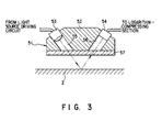
- Fig. 3 shows as an example a detecting head portion 51 of the reflected light amount detecting section 8 included in the toner depositing amount measuring apparatus 42.
- the detecting head portion 51 comprises a supporting member 52 made of an insulating material.
- Formed in the supporting member 52 are a light source 53, a photoelectric converting section 54, an optical path 55 for guiding the light emitted from the light source 53 to the surface of the photosensitive drum 2, and an additional optical path 56 for guiding the light reflected from the surface of the photosensitive drum 2 to the photoelectric converting section 54.
- the bottom surface of the supporting member 52, said bottom surface touching the surface of the photosensitive drum 2 is covered with a transparent plate 57.
- the light emitted from the light source 53 runs through the optical path 55 to reach the surface of the photosensitive drum 2 and, then, is reflected by the surface itself of the photosensitive drum 2 or by the toner fixed after the developing stage.
- the reflected light runs through the optical path 56 to reach the photoelectric converting section 54 so as to be converted into an electric current corresponding to the amount of the reflected light and, then, the current is subjected to a current/voltage conversion.
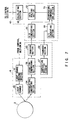
- Fig. 4 shows the construction of the toner depositing amount measuring apparatus 42 according to a first embodiment of the present invention.
- a temperature compensating means is mounted in the reflected light amount detecting section 8.
- the toner depositing amount measuring apparatus 42 can be roughly classified into the reflected light amount detecting section 8 and the toner depositing amount calculating section 43.
- the reflected light amount detecting section 8 comprises the light source 53 serving to irradiate the surface of the photosensitive drum 2 with light emitted therefrom, a light source driving circuit 50 serving to control the driving of the light source 53 based on a control signal generated from the control section 36, the photoelectric converting section 54 which receives the light reflected from the photosensitive drum 2 and converts the received light into an electric signal, a logarithm-compressing section 58 serving to apply a logarithmic calculation to the electric signal generated from the photoelectric converting section, a temperature compensating section 59 provided with a temperature sensitive element (not shown) electrically connected to the logarithm-compressing section 58 to perform compensation of the temperature characteristics of the logarithm-compressing section, and a transfer section 60 for transferring the output signal of the logarithm-compressing section to the toner depositing amount calculating section 43.
- the temperature sensitive element noted above is denoted as a member R3 in Fig. 5.
- the output of the logarithm-compressing section 58 is dependent on temperature
- the output of the logarithm-compressing section 58 tends to be changed greatly depending on the temperature characteristics of the logarithm-compression section 58.
- the temperature compensating section 59 serves to compensate the temperature characteristics of the logarithm-compressing section 58.
- the toner depositing amount calculating section 43 serves to calculate the toner depositing amount on the basis of the signal supplied from the reflected light amount detecting section 8.
- the toner depositing amount calculating section 43 comprised an A/D converting section 61, a data storing section (memory section) 62, and a calculating section 63.
- the signal supplied from the reflected light amount detecting section 8 is converted into a digital signal in the A/D converting section 61.
- the output signal on the surface of the photosensitive drum 2 during non-deposition of the toner and the output signal on the surface of the photosensitive drum 2 during deposition of the toner are stored in the data storing section 62.
- the difference between the data during the toner deposition and the data during non-deposition of the toner, which are stored in the data storing section 62, is calculated in the calculating section 63.
- the toner depositing amount calculating section 43 can be provided singly as an exclusive circuit or, alternatively, can be mounted within the control section 36.
- V PC is the voltage converted from the light reflected from the surface of the photosensitive drum during non-deposition of the toner
- V TN is the voltage converted from the light reflected from the surface of the photosensitive drum during deposition of the toner
- Q is the deposited amount of the toner
- A is a coefficient.
- Fig. 5 shows as an example the electric circuit constituting the logarithm-compressing section 58.
- the logarithm-compressing section 58 comprises a current-voltage converting section 64 and a logarithmic converting section 65.
- the current-voltage converting section 64 includes an operational amplifier OP1 and a photo diode RD acting as a photoelectric converting section 54.
- a current IPD corresponding to the amount of the received light is generated from the photo diode PD and, then, subjected to a current-voltage conversion in the operational amplifier OP1.
- the output signal generated from the current-voltage converting section 64 is subjected to a logarithmic conversion in the logarithmic conversion section 65.
- the logarithmic conversion section 65 comprises, for example, a temperature sensitive resistor element R3 acting as a temperature sensitive element and including a negative resistance element such as a thermistor, operational amplifiers OP2 and OP3, and NPN transistors Tr1 and Tr2 acting as a logarithm characteristic element.
- An output voltage V1 generated from the current-voltage converting section 64 is converted into a current I1 by a resistor R1 included in the logarithmic converting section 65.
- the current ln thus obtained acts as a collector current of the transistor Tr1 serving to perform the logarithmic conversion.
- the operating point of the transistor Tr2 is kept constant by the feedback function of the operational amplifier OP3.
- VE the common emitter voyage of the transistors Tr1 and Tr2
- IS the emitter saturation current (reference current) of the transistors Tr1 and Tr2
- VBE1 the base-emitter voltage of the transistor Trl
- k Boltzman constant
- T absolute temperature
- q charge of electron
- the value of kT/q is 26 mV where the absolute temperature T is 300K (27°C).
- a temperature sensitive resistor element having a temperature coefficient of 0.3%/°C is used as the temperature sensitive resistor element R3.
- Fig. 6 is a graph prepared by using formula (4) given above, i.e., a graph showing the relationship between the output voltage V1 of the current-voltage converting section 64, i.e., the output before the logarithm compression, and the output voltage V0 of the logarithm converting section 65, i.e., the output after the logarithm compression, with the coefficient (proportion gain) set at -A.
- the output voltage V0 from the logarithm converting section 65 is plotted on the ordinate, with the output voltage V1 of the current-voltage converting section 64 being potted on the abscissa.
- the toner deposition amount is diminished with increase in the output voltage V0 after the logarithm compression (upward direction of the ordinate).
- the toner deposition amount is diminished with increase in the output voltage V1 before the logarithm compression (right-ward direction of the abscissa).
- a range of a high concentration region in which the toner deposition amount is large can be broadened by performing the logarithm compression. It is also possible to diminish a range of a low concentration region in which the toner deposition amount is small by performing the logarithm compression.
- a change in the temperature characteristics of transistors is detected by using a temperature sensitive element, i.e., the temperature sensitive resistor element R3.
- the temperature sensitive resistor element R3 is arranged in the vicinity of and is electrically connected to the transistors Tr1 and Tr2 performing a logarithm conversion in a manner to be contradictory to the temperature characteristics of the logarithm-compressing section 58, with the result that the temperature compensation can be performed accurately.
- Fig. 7 shows a toner depositing amount measuring apparatus 42 according to a second embodiment of the present invention.
- the temperature compensation can be achieved without electrically connecting a temperature sensitive element, i.e., the temperature sensitive resistor element R3, to the logarithm-compressing section 58.
- a temperature compensating means is mounted to the toner depositing amount calculating section 43 in this embodiment.
- the toner depositing amount calculating section 43 comprises an A/D converting section 61 serving to convert the signal transferred from the transfer section 60 of the reflected light amount detection section 8 into a digital signal, another A/D converting section 69 serving to convert the signal transferred from the transfer section 68 of the reflected light amount detecting section 8 into a digital signal, a temperature compensating section 70 serving to compensate the temperature characteristics of the output signal generated from the A/D converting section 61 is response to the output signal of the A/D converting section 69, a data holding section (memory section) 62 serving to store the output signal generated from the temperature compensating section 70 in respect of the surface of the photosensitive drum 2 during non-deposition of the toner and the output signal generated from the temperature compensating section 70 in respect of the surface of the photosensitive drum 2 during deposition of the toner, and a calculating section 63 serving to calculate the difference between the data during non-deposition of the toner and the data during deposition of the toner, said data being held in the data holding
- the result of the calculation performed in the calculating section 63 is supplied to the control section 36 as the measured amount of the deposited toner so as to perform various operations including the image density control.
- Fig. 8 shows a toner depositing amount measuring apparatus 42 according to a third embodiment of the present invention.
- a logarithm conversion is performed within the toner depositing amount calculating section 43.
- the reflected light amount detecting section 8 in this embodiment comprises the light source 53 serving to irradiate the surface of the photosensitive drum 2 with light, the light source driving circuit 57 serving to control the driving or the light source 53 in response to a control signal generated from the control section 36, the photoelectric conversion section 54 which receives the light reflected from the surface of the photosensitive drum 2 and converts the received reflected light into an electric signal, and a transfer section 60 serving to transfer the electric signal generated from the photoelectric conversion section 54 to the toner depositing amount calculating section 43.
- Fig. 9 shows the influence given by the non-uniform light reflection from the surface of the photosensitive drum 2.
- the graph of Fig. 9 denotes the changes with the measuring time in the output voltage V1 generated from the current-voltage converting section 54, i.e., the output which is generated when the light reflected from the surface of the photosensitive drum 2 is not subjected to a logarithm-compressing treatment in the case of measuring the reflected light from the surface of the photosensitive drum 2 to which is a toner is not deposited.
- the waveform shown in Fig. 9 represents the influence given by the nonuniform light reflection from the surface of the photosensitive drum 2. It should be noted that the output signal is changed with a period of t1.
- a coating is applied to the surface of the photosensitive drum in order to avoid the image defect caused by an interference lattice stripe.
- the nonuniform coating or the roughening treatment applied to the photosensitive drum cause the particular waveform shown in Fig. 9.
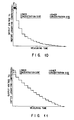
- Fig. 10 shows the output voltage V1 before the logarithm-compressing treatment, which is generated from the current-voltage converting section 64 and corresponds to the amount of the toner deposited on the surface of the photosensitive drum 2.
- Fig. 11 shows the output voltage V0 after the logarithm-compressing treatment, which is generated from the logarithm converting section 65.
- the logarithm compression employed in the present invention permits suppressing the adverse effect produced by the nonuniform light reflection from the surface of the photosensitive drum 2.
- a section 1 shown in each of Figs. 10 and 11 denotes the output owing to the reflected light from the surface of the photosensitive drum 2 itself.
- These drawings show that the toner deposition amount is increased with increase in the measuring time, i.e., toward right-hand region.
- the nonuniform light reflection from the surface or the photosensitive drum 2 in a low concentration region in Fig. 10, which shows the output voltage V1 before the logarithm-compressing treatment is made substantially linear in the changing portion after the logarithm-compressing treatment as shown in Fig. 11. It follows that the adverse effect given by the nonuniform light reflection can be diminished by the logarithm-compressing treatment employed in the present invention.
- the graph of Fig. 6 shows that a range is diminished in the low concentration region. This is because it is possible to diminish the width of change in respect of the change in the output signal such as the nununiform light reflection from the photosensitive drum 2.
- Figs. 10 and 11 clearly show the effect produced by the logarithm compression applied to the output generated from the reflected light amount detecting section 8 in a high concentration region.
- Fig. 10 shows the output voltage V1 generated from the current-voltage converting section 64, which is not subjected to a logarithm-compressing treatment, with Fig. 11 showing the output voltage V0 generated from the logarithm converting section 65 after application of the logarithm-compressing treatment.
- Fig. 10 shows that, in the low concentration region, a large difference is generated between two adjacent data in the level of the output voltage V1 generated from the current-voltage converting section 64 before application of the logarithm-compressing treatment.
- a difference between two adjacent data in the level of the output voltage V1 is rendered substantially negligible.
- the effect produced by the logarithm-compressing treatment can by clearly seen from Fig. 11. Specifically, it is shown that a difference in the level of the output voltage VO after the logarithm-compressing treatment is enlarged between two adjacent data in the high concentration region, compared with the data shown in Fig. 10, though the difference is diminished in the low concentration region in Fig. 11. In other words, the difference in the level of the output voltage between two adjacent data in Fig. 11 is substantially equal to that in Fig. 10. It follows that the logarithm-compressing treatment employed in the present invention makes it possible to suppress the adverse effect given by the nonuniform light reflection from the photosensitive drum 2 and to improve the dynamic range.
- the present invention provided an image forming apparatus which permits overcoming the defects inherent in the conventional apparatus.
- the present invention makes it possible to diminish the measuring error caused by the nonuniform light reflection from an image carrier and to enlarge the dynamic range with respect to the light reflecting characteristics of a developing agent. It follows that it is possible to suppress the deterioration in the measuring accuracy caused by the mixing or a noise in the step of transferring the signal denoting the result of measurement. Further, the changes in the characteristics of the logarithm-compressing means, which are caused by the change in temperature, can be canceled in the present invention so as to control the image density with a high accuracy, making it possible to maintain a high image quality.
Landscapes
- Physics & Mathematics (AREA)
- General Physics & Mathematics (AREA)
- Spectroscopy & Molecular Physics (AREA)
- Engineering & Computer Science (AREA)
- Microelectronics & Electronic Packaging (AREA)
- Control Or Security For Electrophotography (AREA)
- Investigating Materials By The Use Of Optical Means Adapted For Particular Applications (AREA)
- Dry Development In Electrophotography (AREA)
Claims (8)
- Bildausbildungsgerät, das folgendes aufweist:eine Einrichtung (13) zum Ausbilden eines Bildes auf einem Bildträger (2), wobei das Bild Bilddaten entspricht, die mit einem Entwicklungsmittel unter einer vorbestimmten Bildausbildungsbedingung gebildet sind;eine Einrichtung (42) zum Erfassen der am Bildträger angebrachten Menge an Entwicklungsmittel; undeine Einrichtung (36) zum Einstellen der Bildausbildungsbedingung in Übereinstimmung mit der durch die Erfassungseinrichtung erfaßten Menge an Entwicklungsmittel, um Bilddichteänderungen des auf dem Bildträger ausgebildeten Bildes zu stabilisieren,wobei die Erfassungseinrichtung folgendes aufweist:a) eine Einrichtung (53) zum Richten eines Lichtstrahls in Richtung zu einer Oberfläche des Bildträgers;b) eine Einrichtung (54) zum Umwandeln des von der Oberfläche des Bildträgers reflektierten Lichts in elektrische Signale; undwobei das Gerät weiterhin folgendes aufweist:
c) eine Einrichtung (58; 71) zum logarithmischen Komprimieren der durch die Umwandlungseinrichtung erzeugten Signale;
dadurch gekennzeichnet, daß
die Umwandlungseinrichtung (54) eine Umwandlung durchführt, um die Beziehung V = kP zu erfüllen, wobei V eine Spannung anzeigt, k einen Koeffizienten bezeichnet, und P das reflektierte Licht darstellt, und somit die Spannung V proportional zur Menge P des reflektierten Lichts ist; und
wobei die Erfassungseinrichtung weiterhin folgendes aufweist:
d) eine Einrichtung (43) zum Berechnen einer Entwicklungsmittel-Ablagerungsmenge in Übereinstimmung mit einer Differenz zwischen Daten, die während einer Ablagerung eines Entwicklungsmittels am Bildträger geliefert werden, und Daten, die während keiner Ablagerung eines Entwicklungsmittels am Bildträger geliefert werden. - Bildausbildungsgerät nach Anspruch 1, gekennzeichnet durch eine Einrichtung (59) zum Kompensieren der Temperaturcharakteristiken der Logarithmus-Kompressionseinrichtung, wobei die Kompensationseinrichtung (59) ein temperaturempfindliches Element (67; R3) aufweist, das elektrisch auf die Umgebungstemperatur reagiert, und die Kompensationseinrichtung (59) weiterhin einen Temperaturkompensationsabschnitt zum Kompensieren der Temperaturcharakteristiken der Logarithmus-Kompressionseinrichtung (58) gemäß dem durch das temperaturempfindliche Element erzeugten Ausgangssignal aufweist.
- Bildausbildungsgerät nach Anspruch 2, dadurch gekennzeichnet, daß das temperaturempfindliche Element (R3) mit der Logarithmus-Kompressionseinrichtung (58) elektrisch verbunden ist, um die Temperaturcharakteristiken der Logarithmus-Kompressionseinrichtung auszulöschen.
- Bildausbildungsgerät nach Anspruch 2, dadurch gekennzeichnet, daß das temperaturempfindliche Element (67) nicht mit der Logarithmus-Kompressionseinrichtung (58) verbunden ist.
- Bildausbildungsgerät nach einem der vorangehenden Ansprüche, dadurch gekennzeichnet, daß die Berechnungseinrichtung (43) folgendes enthält:eine A/D-Wandlereinrichtung (61) zum Umwandeln des ersten und des zweiten Ausgangssignals, die durch die Logarithmus-Kompressionseinrichtung (58) erzeugt sind, in ein erstes und ein zweites digitales Signal;eine Halteeinrichtung (62) zum Halten des ersten und des zweiten digitalen Signals, die durch die A/D-Wandlereinrichtung umgewandelt sind; undeine Berechnungseinrichtung (63) zum Berechnen einer Differenz zwischen dem ersten und dem zweiten digitalen Signal, die durch die Halteeinrichtung gehalten sind.
- Bildausbildungsgerät nach einem der vorangehenden Ansprüche, dadurch gekennzeichnet, daß die Logarithmus-Kompressionseinrichtung (58) ein logarithmuscharakteristisches Element (Tr2) mit einer Temperaturabhängigkeit enthält.
- Bildausbildungsgerät nach Anspruch 6, wenn Anspruch 6 von einem der Ansprüche 2 bis 5 abhängt, dadurch gekennzeichnet, daß das temperaturempfindliche Element (R3) eine Temperaturabhängigkeit hat, die entgegengesetzt zu jener des logarithmus-charakteristischen Elements ist.
- Bildausbildungsgerät nach Anspruch 7, dadurch gekennzeichnet, daß das temperaturempfindliche Element (R3) mit dem logarithmus-charakteristischen Element (Tr2) thermisch gekoppelt ist.
Applications Claiming Priority (2)
| Application Number | Priority Date | Filing Date | Title |
|---|---|---|---|
| JP255081/92 | 1992-09-24 | ||
| JP4255081A JPH06109643A (ja) | 1992-09-24 | 1992-09-24 | 画像形成装置 |
Publications (3)
| Publication Number | Publication Date |
|---|---|
| EP0589129A2 EP0589129A2 (de) | 1994-03-30 |
| EP0589129A3 EP0589129A3 (en) | 1994-08-10 |
| EP0589129B1 true EP0589129B1 (de) | 1997-10-22 |
Family
ID=17273870
Family Applications (1)
| Application Number | Title | Priority Date | Filing Date |
|---|---|---|---|
| EP93104521A Expired - Lifetime EP0589129B1 (de) | 1992-09-24 | 1993-03-19 | Bilderzeugungsgerät zur Kontrolle der Dichte eines Bildes mit logarithmischen Kompressionsmitteln |
Country Status (4)
| Country | Link |
|---|---|
| US (1) | US5365313A (de) |
| EP (1) | EP0589129B1 (de) |
| JP (1) | JPH06109643A (de) |
| DE (1) | DE69314741T2 (de) |
Families Citing this family (12)
| Publication number | Priority date | Publication date | Assignee | Title |
|---|---|---|---|---|
| JPH0758958A (ja) * | 1993-07-01 | 1995-03-03 | Xerox Corp | グレイ画素ハーフトーンシステム及びカラー印刷におけるトナーデポジションの制御 |
| US5873011A (en) * | 1996-03-13 | 1999-02-16 | Minolta Co., Ltd. | Image forming apparatus |
| US6092032A (en) * | 1997-03-12 | 2000-07-18 | Nitto Kogyo Co., Ltd. | Electroconductive roller and apparatus and method for testing it |
| US5822662A (en) * | 1997-04-09 | 1998-10-13 | Xerox Corporation | Background detection and compensation |
| JPH11265112A (ja) * | 1998-03-17 | 1999-09-28 | Minolta Co Ltd | 画像形成装置 |
| JP2002006683A (ja) * | 2000-06-26 | 2002-01-11 | Sharp Corp | トナー濃度センサ |
| JP4143253B2 (ja) * | 2000-10-04 | 2008-09-03 | 株式会社リコー | 画像形成装置 |
| JP3516943B2 (ja) * | 2001-12-18 | 2004-04-05 | 東芝テック株式会社 | トナー付着量測定装置および着色剤付着量測定装置 |
| US6909858B2 (en) * | 2002-08-09 | 2005-06-21 | Seiko Epson Corporation | Image forming apparatus, toner-adhesion calculation method and data processing method |
| JP2008058157A (ja) | 2006-08-31 | 2008-03-13 | Brother Ind Ltd | 光量測定装置、画像形成装置およびトナー濃度測定装置 |
| US20090135449A1 (en) * | 2007-11-27 | 2009-05-28 | Kabushiki Kaisha Toshiba | Image forming apparatus |
| JP6136614B2 (ja) * | 2013-06-14 | 2017-05-31 | 株式会社リコー | 透磁率検知器、透磁率検知器の取り付け方法、現像装置 |
Family Cites Families (18)
| Publication number | Priority date | Publication date | Assignee | Title |
|---|---|---|---|---|
| JPS5161243A (en) * | 1974-11-25 | 1976-05-27 | Fuji Photo Optical Co Ltd | Taisuzofukuki |
| JPS52106054U (de) * | 1976-02-09 | 1977-08-12 | ||
| JPS54143144A (en) * | 1978-04-14 | 1979-11-08 | Konishiroku Photo Ind Co Ltd | Image density detecting method and apparatus for zerographic copier |
| US4277162A (en) * | 1978-07-13 | 1981-07-07 | Ricoh Company, Ltd. | Electrophotographic apparatus comprising density sensor means |
| US4318610A (en) * | 1980-04-21 | 1982-03-09 | Xerox Corporation | Control system for an electrophotographic printing machine |
| JPS5818644A (ja) * | 1981-07-27 | 1983-02-03 | Konishiroku Photo Ind Co Ltd | 画像記録装置 |
| US4550254A (en) * | 1984-01-16 | 1985-10-29 | Xerox Corporation | Low cost infrared reflectance densitometer signal processor chip |
| EP0223880A1 (de) * | 1985-10-30 | 1987-06-03 | Agfa-Gevaert N.V. | Optoelektronische Schaltung zur Erzeugung eines Bildkontrastsignals |
| US4801980A (en) * | 1986-10-29 | 1989-01-31 | Konica Corporation | Toner density control apparatus |
| US4870460A (en) * | 1986-12-05 | 1989-09-26 | Ricoh Company, Ltd. | Method of controlling surface potential of photoconductive element |
| GB2212419B (en) * | 1987-12-25 | 1991-12-04 | Ricoh Kk | Image density control method and color image forming apparatus |
| JPH01306874A (ja) * | 1988-06-03 | 1989-12-11 | Ricoh Co Ltd | 電子写真装置の画像制御方法 |
| JP2918045B2 (ja) * | 1988-10-28 | 1999-07-12 | 株式会社リコー | 画像濃度制御装置 |
| JPH02125270A (ja) * | 1988-11-04 | 1990-05-14 | Ricoh Co Ltd | 複写制御装置 |
| US5099279A (en) * | 1989-08-10 | 1992-03-24 | Minolta Camera Kabushiki Kaisha | Image forming method and image forming apparatus in which the density of the toner image is measured and controlled |
| EP0443535A3 (en) * | 1990-02-21 | 1992-10-28 | Tokyo Electric Co., Ltd. | Electrophotographic printing apparatus |
| US5148217A (en) * | 1991-06-24 | 1992-09-15 | Eastman Kodak Company | Electrostatographic copier/printer densitometer insensitive to power supply variations |
| US5208655A (en) * | 1991-08-07 | 1993-05-04 | Graphics Microsystems, Inc. | Method and apparatus for automatic densitometer alignment |
-
1992
- 1992-09-24 JP JP4255081A patent/JPH06109643A/ja active Pending
-
1993
- 1993-03-17 US US08/032,299 patent/US5365313A/en not_active Expired - Fee Related
- 1993-03-19 EP EP93104521A patent/EP0589129B1/de not_active Expired - Lifetime
- 1993-03-19 DE DE69314741T patent/DE69314741T2/de not_active Expired - Fee Related
Non-Patent Citations (2)
| Title |
|---|
| 306 874 (RICOH) 11 December 1989 * |
| PATENT ABSTRACTS OF JAPAN vol. 14, no. 101 (P-1012) 23 February 1990 & JP-A-01 * |
Also Published As
| Publication number | Publication date |
|---|---|
| EP0589129A2 (de) | 1994-03-30 |
| US5365313A (en) | 1994-11-15 |
| DE69314741D1 (de) | 1997-11-27 |
| JPH06109643A (ja) | 1994-04-22 |
| EP0589129A3 (en) | 1994-08-10 |
| DE69314741T2 (de) | 1998-03-12 |
Similar Documents
| Publication | Publication Date | Title |
|---|---|---|
| US6121986A (en) | Process control for electrophotographic recording | |
| JP2619218B2 (ja) | 現像装置の経時劣化によるトナー濃度ドリフトに対する自動補償方法 | |
| JPH0128940B2 (de) | ||
| US5365313A (en) | Image forming apparatus for controlling image density using logarithm compressing means | |
| US5937229A (en) | Image forming apparatus and method with control of electrostatic transfer using constant current | |
| JPH052305A (ja) | 画像形成装置 | |
| JPH11258872A (ja) | 電子写真装置 | |
| EP0223880A1 (de) | Optoelektronische Schaltung zur Erzeugung eines Bildkontrastsignals | |
| US5477312A (en) | Method of controlling image density | |
| US5659841A (en) | Electrostatic recording control method and electrostatic recording apparatus | |
| US4563081A (en) | Apparatus for controlling image forming condition | |
| JPH05119567A (ja) | 画像形成装置 | |
| US5987271A (en) | Method and apparatus for control of variability in charge to mass ratio in a development station | |
| US6559876B2 (en) | Image forming apparatus with exposure reduction mode | |
| US5862433A (en) | Electrostatographic method and apparatus with improved auto cycle up | |
| JP3740850B2 (ja) | 光学的検出装置及びその方法、並びに画像濃度制御装置 | |
| US5574543A (en) | Image forming apparatus | |
| US6055011A (en) | Image processing apparatus which performs density control for each of plural colors of recording material | |
| US5568234A (en) | Image density control device | |
| JPH06110286A (ja) | 画像形成装置 | |
| US5497221A (en) | Method of adjusting image density parameters by repetitively adjusting image density parameter values based upon reference pattern density at standby time intervals | |
| JP3218197B2 (ja) | トナー濃度センサ装置 | |
| JPH08262817A (ja) | 画像記録装置の濃度制御方法 | |
| JPH06110285A (ja) | 画像形成装置 | |
| JP3516943B2 (ja) | トナー付着量測定装置および着色剤付着量測定装置 |
Legal Events
| Date | Code | Title | Description |
|---|---|---|---|
| PUAI | Public reference made under article 153(3) epc to a published international application that has entered the european phase |
Free format text: ORIGINAL CODE: 0009012 |
|
| 17P | Request for examination filed |
Effective date: 19930319 |
|
| AK | Designated contracting states |
Kind code of ref document: A2 Designated state(s): DE FR GB |
|
| PUAL | Search report despatched |
Free format text: ORIGINAL CODE: 0009013 |
|
| AK | Designated contracting states |
Kind code of ref document: A3 Designated state(s): DE FR GB |
|
| 17Q | First examination report despatched |
Effective date: 19960119 |
|
| GRAG | Despatch of communication of intention to grant |
Free format text: ORIGINAL CODE: EPIDOS AGRA |
|
| GRAH | Despatch of communication of intention to grant a patent |
Free format text: ORIGINAL CODE: EPIDOS IGRA |
|
| GRAH | Despatch of communication of intention to grant a patent |
Free format text: ORIGINAL CODE: EPIDOS IGRA |
|
| GRAA | (expected) grant |
Free format text: ORIGINAL CODE: 0009210 |
|
| AK | Designated contracting states |
Kind code of ref document: B1 Designated state(s): DE FR GB |
|
| REF | Corresponds to: |
Ref document number: 69314741 Country of ref document: DE Date of ref document: 19971127 |
|
| ET | Fr: translation filed | ||
| PLBE | No opposition filed within time limit |
Free format text: ORIGINAL CODE: 0009261 |
|
| 26N | No opposition filed | ||
| REG | Reference to a national code |
Ref country code: GB Ref legal event code: 746 Effective date: 19981008 |
|
| PGFP | Annual fee paid to national office [announced via postgrant information from national office to epo] |
Ref country code: FR Payment date: 19990309 Year of fee payment: 7 |
|
| REG | Reference to a national code |
Ref country code: FR Ref legal event code: D6 |
|
| PGFP | Annual fee paid to national office [announced via postgrant information from national office to epo] |
Ref country code: GB Payment date: 19990318 Year of fee payment: 7 |
|
| PGFP | Annual fee paid to national office [announced via postgrant information from national office to epo] |
Ref country code: DE Payment date: 19990326 Year of fee payment: 7 |
|
| PG25 | Lapsed in a contracting state [announced via postgrant information from national office to epo] |
Ref country code: GB Free format text: LAPSE BECAUSE OF NON-PAYMENT OF DUE FEES Effective date: 20000319 |
|
| GBPC | Gb: european patent ceased through non-payment of renewal fee |
Effective date: 20000319 |
|
| PG25 | Lapsed in a contracting state [announced via postgrant information from national office to epo] |
Ref country code: FR Free format text: LAPSE BECAUSE OF NON-PAYMENT OF DUE FEES Effective date: 20001130 |
|
| REG | Reference to a national code |
Ref country code: FR Ref legal event code: ST |
|
| PG25 | Lapsed in a contracting state [announced via postgrant information from national office to epo] |
Ref country code: DE Free format text: LAPSE BECAUSE OF NON-PAYMENT OF DUE FEES Effective date: 20010103 |