EP0589124B1 - Method for eliminating the bird's beak from selective oxidations of semiconductor electronic devices - Google Patents
Method for eliminating the bird's beak from selective oxidations of semiconductor electronic devices Download PDFInfo
- Publication number
- EP0589124B1 EP0589124B1 EP92830514A EP92830514A EP0589124B1 EP 0589124 B1 EP0589124 B1 EP 0589124B1 EP 92830514 A EP92830514 A EP 92830514A EP 92830514 A EP92830514 A EP 92830514A EP 0589124 B1 EP0589124 B1 EP 0589124B1
- Authority
- EP
- European Patent Office
- Prior art keywords
- oxide
- nitride
- layer
- seat
- trench
- Prior art date
- Legal status (The legal status is an assumption and is not a legal conclusion. Google has not performed a legal analysis and makes no representation as to the accuracy of the status listed.)
- Expired - Lifetime
Links
Images

Classifications
-
- H—ELECTRICITY
- H10—SEMICONDUCTOR DEVICES; ELECTRIC SOLID-STATE DEVICES NOT OTHERWISE PROVIDED FOR
- H10W—GENERIC PACKAGES, INTERCONNECTIONS, CONNECTORS OR OTHER CONSTRUCTIONAL DETAILS OF DEVICES COVERED BY CLASS H10
- H10W10/00—Isolation regions in semiconductor bodies between components of integrated devices
- H10W10/10—Isolation regions comprising dielectric materials
- H10W10/13—Isolation regions comprising dielectric materials formed using local oxidation of silicon [LOCOS], e.g. sealed interface localised oxidation [SILO] or side-wall mask isolation [SWAMI]
-
- H—ELECTRICITY
- H10—SEMICONDUCTOR DEVICES; ELECTRIC SOLID-STATE DEVICES NOT OTHERWISE PROVIDED FOR
- H10P—GENERIC PROCESSES OR APPARATUS FOR THE MANUFACTURE OR TREATMENT OF DEVICES COVERED BY CLASS H10
- H10P14/00—Formation of materials, e.g. in the shape of layers or pillars
- H10P14/60—Formation of materials, e.g. in the shape of layers or pillars of insulating materials
- H10P14/61—Formation of materials, e.g. in the shape of layers or pillars of insulating materials using masks
-
- H—ELECTRICITY
- H10—SEMICONDUCTOR DEVICES; ELECTRIC SOLID-STATE DEVICES NOT OTHERWISE PROVIDED FOR
- H10W—GENERIC PACKAGES, INTERCONNECTIONS, CONNECTORS OR OTHER CONSTRUCTIONAL DETAILS OF DEVICES COVERED BY CLASS H10
- H10W10/00—Isolation regions in semiconductor bodies between components of integrated devices
- H10W10/01—Manufacture or treatment
- H10W10/011—Manufacture or treatment of isolation regions comprising dielectric materials
- H10W10/012—Manufacture or treatment of isolation regions comprising dielectric materials using local oxidation of silicon [LOCOS]
- H10W10/0121—Manufacture or treatment of isolation regions comprising dielectric materials using local oxidation of silicon [LOCOS] in regions recessed from the surface, e.g. in trenches or grooves
Definitions
- This invention relates to a method for eliminating the bird's beak from selective oxidations of semiconductor electronic devices.
- the invention relates to a method applied to semiconductor devices having a semiconductor substrate covered by an oxide layer which is covered, in turn, by a first layer of nitride, and wherein at least one pit is opened for growing an isolation region therein.
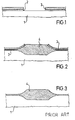
- LOCOS silicon local oxidation technology
- An oxide layer 2 is grown over a substrate 1 of semiconductor silicon.
- the oxide 2 is then covered with a nitride layer 3, and a subsequent phototechnique step results in the active areas of the device being defined.
- the above-outlined LOCOS technology invariably leaves a so-called bird's beak whose length is approximately 85% of the grown oxide thickness.
- SWAMI Silicon Masked Isolation Technology
- the last-mentioned process involves at least two separate oxidation steps, of which the first still results in the development of a bird's beak of significant size.
- This document relates to the possibility of partially preventing the formation of "bird's beak” while growing oxide isolation regions in a semiconductor body by using small undercuts in an oxide layer filled with nitride.
- This semiconductor body is formed by growing a first oxide layer on a semiconductor substrate and covering this first layer by a first nitride layer.
- a selective etching step is performed to create the undercuts.
- a deposition of second nitride layer is required to fill the undercuts.
- the thickness of the second nitride layer being slightly greater than half the thickness of the slide layer.
- the semiconductor body is then subjected to a vertical reactive ion etching step to etch away portions of the second nitride layer with the exception of the undercuts.
- a depression is formed in the seminconductor body by a coventional silicon etching where the recessed oxide can be grown.
- the undercuts filled with nitride doesn't allow migration of oxygen, and hence formation of the bird's beak.
- the solution hereby uses an anisotropic etch to define exactly which parts of sidewalls must be protected by nitride.
- the nitride layer used to fill the undercuts is removed by isotropic wet etching performed with ortophosforic acid.
- the underlying technical problem of this invention is to provide a method for eliminating the so-called bird's beak from local oxidations, while overcoming the limitations of current approaches based on prior art techniques.
- the solutive idea on which this invention stands is one of only avoiding that in the seat or in the trench seat where the oxide is to be grown a complete removing of the second nitride layer is obtained except from the recesses which remain occluded by nitride portion.
- the device comprises a monocrystalline silicon substrate 1 over which a layer 2 of silicon thermal oxide has been grown.
- the oxide 2 is covered by a first layer 3 of silicon nitride.
- a pit 7 is opened through the layers 2 and 3 to the substrate 1. This pit 7 is intended to provide an isolation region, such as a field oxide region.
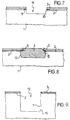
- Shown in Figure 4 is a semiconductor device which comprises the substrate 1, layer 2 of thermal oxide and first upper layer 3 of nitride.
- the device has been formed with an pit 11.
- this pit 11 is also dug in the substrate 1 to define a seat 12 for receiving an isolation region 4 consisting of field oxide.
- the inventive method provides, for selective wet etching, using diluted hydrofluoric acid. This etching only causes the thermal oxide 2 to be dug laterally of the pit 11, as shown in Figure 5.
- the etching is only effective in the pit area unprotected by the nitride 3 and defines opposing recesses 6 and 8 at the pit 11 sides.
- the digging depth will depend on the etching duration.
- the next step consists of depositing a second layer 5 of silicon nitride.
- This second layer of nitride has a thickness slightly greater than one half that of the thermal oxide layer 2.
- the nitride of the layer 5 also penetrates the recesses 6 and 8, obstructing them.
- a subsequent etching step as by etching with orthophosphoric acid, enables the nitride layer 5 to be removed, except from the recesses 6 and 8 which will remain occluded by residues 9 and 10.
- nitride occlusions is effective to resist formation of the bird's beak while the field oxide 4 is grown.
- This example relates specifically to a possible embodiment of the inventive method directed to allow the formation of sidewall oxide in a trench-type structure.
- a semiconductor substrate 1 is provided as in the previous embodiments which is covered by a layer 2 of thermal oxide, in turn covered by a first layer 3 of nitride.
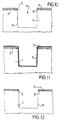
- the semiconductor is formed with a deep pit 13, or so-called trench pit ( Figure 9), defining a seat 15 whereinto the so-called sidewall oxide is received.
- the etching is only effective in the uncovered area, unprotected by the nitride 3, and defines oppositely located recesses 6 and 8 at the sides of the pit 13.
- the digging depth will depend on the duration of the etching applied.
- the next step in the method consists of depositing a second layer 5 of silicon nitride.
- This, the second, layer of nitride slightly exceeds in thickness one half of the thermal oxide layer 2 thickness.
- the layer 5 nitride is deposited isotropically across the side walls of the pit 13 and also penetrates the recesses 6 and 8, obstructing them.
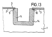
- a subsequent etching step enables the nitride layer 5 to be removed, excepting from the recesses 6 and 8 which remain occluded by residues 9 and 10. At this point, the sidewall oxide 14 is grown on the inner walls of the seat 15.
- the semiconductor structure may be completed with the addition of active areas within the region bounded by the sidewall oxide.
- the major advantages afforded by the method of this invention include the possibility of enhancing the degree of integration of semiconductor electronic devices.
Landscapes
- Local Oxidation Of Silicon (AREA)
- Element Separation (AREA)
Description
- Figures 1 to 3 are respective views showing schematically the production of a local oxidation on a semiconductor device;
- Figures 4 to 8 show schematically a exemplary application of the inventive method, specifically to nonplanar structures; and
- Figures 9 to 13 show schematically a second embodiment of the method according to the invention.
Claims (2)
- A method for eliminating the bird's beak while forming recessed oxide regions by selective oxidation in a semiconductor body having a semiconductor substrate (1) which is covered by an oxide layer (2) and with a first nitride layer (3) formed on the oxide layer (2), comprising the following steps:opening a pit (11) or a trench pit (13) through the nitride layer (3) and the oxide layer (3) by a first etching step to define a recessed seat or trench (12, 13) in said semiconductor substrate (1) for growing an isolation region (4) including field oxide into said seat or a sidewall oxide (14) region into said trench (15),selectively wet etching the oxide layer (2) to remove it around the sides of said seat (12) or trench (13) between the substrate (1) and the first nitride layer (3) to define peripheral recesses (6,8) or undercuts between the substrate (1) and the first nitride layer (3);depositing a second nitride layer (5) extending into the interior of the seat (12) or the trench (13), occluding said undercuts (6, 8) with nitride, the thickness of the second nitride layer (5) being slightly greater than half the thickness of the oxide layer (2); and,subsequently etching said second nitride layer (5) to remove it with the exception of the undercuts (6, 8) which remains occluded by nitride portions (9, 10); andgrowing oxide in said seat (12) or trench (13) so as to form said isolation region (4) including field oxide containing or respective sidewall (14) oxide regions abutting said nitride portions (9,10) which occlude said recesses (6,8).
- A method according to claim 1, characterized in that said subsequent etching step is performed by using orthophosphoric acid.
Priority Applications (4)
| Application Number | Priority Date | Filing Date | Title |
|---|---|---|---|
| DE69228117T DE69228117T2 (en) | 1992-09-23 | 1992-09-23 | Method for preventing the bird's beak during the selective oxidation of semiconductor electronic devices |
| EP92830514A EP0589124B1 (en) | 1992-09-23 | 1992-09-23 | Method for eliminating the bird's beak from selective oxidations of semiconductor electronic devices |
| US08/124,695 US5504034A (en) | 1992-09-23 | 1993-09-20 | Local oxidation method with bird's beak suppression |
| JP5234836A JPH06295954A (en) | 1992-09-23 | 1993-09-21 | Method for eliminating bird's beak from processing method and selective oxidation of semiconductor electronic element |
Applications Claiming Priority (1)
| Application Number | Priority Date | Filing Date | Title |
|---|---|---|---|
| EP92830514A EP0589124B1 (en) | 1992-09-23 | 1992-09-23 | Method for eliminating the bird's beak from selective oxidations of semiconductor electronic devices |
Publications (2)
| Publication Number | Publication Date |
|---|---|
| EP0589124A1 EP0589124A1 (en) | 1994-03-30 |
| EP0589124B1 true EP0589124B1 (en) | 1999-01-07 |
Family
ID=8212179
Family Applications (1)
| Application Number | Title | Priority Date | Filing Date |
|---|---|---|---|
| EP92830514A Expired - Lifetime EP0589124B1 (en) | 1992-09-23 | 1992-09-23 | Method for eliminating the bird's beak from selective oxidations of semiconductor electronic devices |
Country Status (4)
| Country | Link |
|---|---|
| US (1) | US5504034A (en) |
| EP (1) | EP0589124B1 (en) |
| JP (1) | JPH06295954A (en) |
| DE (1) | DE69228117T2 (en) |
Families Citing this family (13)
| Publication number | Priority date | Publication date | Assignee | Title |
|---|---|---|---|---|
| JPH0897202A (en) * | 1994-09-22 | 1996-04-12 | Fujitsu Ltd | Method for manufacturing semiconductor device |
| US5455194A (en) * | 1995-03-06 | 1995-10-03 | Motorola Inc. | Encapsulation method for localized oxidation of silicon with trench isolation |
| KR0179807B1 (en) * | 1995-12-30 | 1999-03-20 | 문정환 | Method of manufacturing semiconductor memory device |
| US5891788A (en) * | 1996-11-14 | 1999-04-06 | Micron Technology, Inc. | Locus isolation technique using high pressure oxidation (hipox) and protective spacers |
| TW388100B (en) * | 1997-02-18 | 2000-04-21 | Hitachi Ulsi Eng Corp | Semiconductor deivce and process for producing the same |
| US6399462B1 (en) * | 1997-06-30 | 2002-06-04 | Cypress Semiconductor Corporation | Method and structure for isolating integrated circuit components and/or semiconductor active devices |
| KR100247939B1 (en) * | 1997-09-08 | 2000-03-15 | 윤종용 | Device Separation Method of Semiconductor Device Using Second Pad Oxide by Chemical Vapor Deposition |
| TW415018B (en) * | 1997-10-18 | 2000-12-11 | United Microelectronics Corp | Manufacture of LOCOS |
| JP3955404B2 (en) * | 1998-12-28 | 2007-08-08 | 株式会社ルネサステクノロジ | Manufacturing method of semiconductor integrated circuit device |
| JP3751469B2 (en) * | 1999-04-26 | 2006-03-01 | 沖電気工業株式会社 | Manufacturing method of semiconductor device having SOI structure |
| US20070224838A1 (en) * | 2006-03-27 | 2007-09-27 | Honeywell International Inc. | Method of straining a silicon island for mobility improvement |
| CN101359615B (en) * | 2007-07-30 | 2010-08-11 | 中芯国际集成电路制造(上海)有限公司 | Semiconductor isolation structure and manufacturing method of semiconductor device |
| CN112086352B (en) * | 2020-08-06 | 2024-02-20 | 北京晶亦精微科技股份有限公司 | A process for growing oxide isolation layers and preparing IGBT chips using Locos |
Family Cites Families (9)
| Publication number | Priority date | Publication date | Assignee | Title |
|---|---|---|---|---|
| EP0052948A1 (en) * | 1980-11-24 | 1982-06-02 | Motorola, Inc. | Oxide isolation process |
| US4563227A (en) * | 1981-12-08 | 1986-01-07 | Matsushita Electric Industrial Co., Ltd. | Method for manufacturing a semiconductor device |
| JPS5994844A (en) * | 1982-11-24 | 1984-05-31 | Nec Corp | Manufacture of semiconductor device |
| JPS6021541A (en) * | 1983-07-15 | 1985-02-02 | Nec Corp | Manufacture of semiconductor device |
| JPS61296741A (en) * | 1985-06-25 | 1986-12-27 | Nec Corp | Manufacture of semiconductor device |
| JPH079930B2 (en) * | 1985-07-10 | 1995-02-01 | 松下電子工業株式会社 | Method for manufacturing semiconductor device |
| JPS62133732A (en) * | 1985-12-06 | 1987-06-16 | Nec Corp | Manufacture of semiconductor device |
| NL8601415A (en) * | 1986-06-02 | 1988-01-04 | Philips Nv | METHOD FOR MANUFACTURING A SEMICONDUCTOR DEVICE |
| EP0518418A1 (en) * | 1991-06-10 | 1992-12-16 | Koninklijke Philips Electronics N.V. | Method of manufacturing a semiconductor device whereby field oxide regions are formed in a surface of a silicon body through oxidation |
-
1992
- 1992-09-23 EP EP92830514A patent/EP0589124B1/en not_active Expired - Lifetime
- 1992-09-23 DE DE69228117T patent/DE69228117T2/en not_active Expired - Fee Related
-
1993
- 1993-09-20 US US08/124,695 patent/US5504034A/en not_active Expired - Lifetime
- 1993-09-21 JP JP5234836A patent/JPH06295954A/en active Pending
Also Published As
| Publication number | Publication date |
|---|---|
| DE69228117D1 (en) | 1999-02-18 |
| DE69228117T2 (en) | 1999-05-20 |
| JPH06295954A (en) | 1994-10-21 |
| US5504034A (en) | 1996-04-02 |
| EP0589124A1 (en) | 1994-03-30 |
Similar Documents
| Publication | Publication Date | Title |
|---|---|---|
| USRE35294E (en) | Polysilicon encapsulated localized oxidation of silicon | |
| US5470781A (en) | Method to reduce stress from trench structure on SOI wafer | |
| EP0146789B1 (en) | Process for forming isolating trenches in integrated circuit devices | |
| EP0488625B1 (en) | Method for use in a semiconductor field oxidation process | |
| US4900692A (en) | Method of forming an oxide liner and active area mask for selective epitaxial growth in an isolation trench | |
| US5326715A (en) | Method for forming a field oxide film of a semiconductor device | |
| JPS6340337A (en) | Method of isolating integrated circuit | |
| US6033969A (en) | Method of forming a shallow trench isolation that has rounded and protected corners | |
| EP0589124A1 (en) | Method for eliminating the bird's beak from selective oxidations of semiconductor electronic devices | |
| US5512509A (en) | Method for forming an isolation layer in a semiconductor device | |
| US20030176043A1 (en) | Shallow trench isolation approach for improved STI corner rounding | |
| US5937310A (en) | Reduced bird's beak field oxidation process using nitrogen implanted into active region | |
| US5432118A (en) | Process for forming field isolation | |
| US5681776A (en) | Planar selective field oxide isolation process using SEG/ELO | |
| US5629230A (en) | Semiconductor processing method of forming field oxide regions on a semiconductor substrate utilizing a laterally outward projecting foot portion | |
| JPS61101047A (en) | Planox method with reduced formation of beak part for forming integrated electronic component element | |
| US5371035A (en) | Method for forming electrical isolation in an integrated circuit device | |
| EP0641022B1 (en) | Isolation structure and method for making same | |
| EP0773582A3 (en) | Method of forming a trench isolation structure in an integrated circuit | |
| EP0424018A2 (en) | Integrated circuit field isolation process | |
| US5962914A (en) | Reduced bird's beak field oxidation process using nitrogen implanted into active region | |
| US5696022A (en) | Method for forming field oxide isolation film | |
| US5846596A (en) | Methods of forming field oxide isolation regions having sloped edges | |
| US6265286B1 (en) | Planarization of LOCOS through recessed reoxidation techniques | |
| US6579777B1 (en) | Method of forming local oxidation with sloped silicon recess |
Legal Events
| Date | Code | Title | Description |
|---|---|---|---|
| PUAI | Public reference made under article 153(3) epc to a published international application that has entered the european phase |
Free format text: ORIGINAL CODE: 0009012 |
|
| AK | Designated contracting states |
Kind code of ref document: A1 Designated state(s): DE FR GB IT |
|
| 17P | Request for examination filed |
Effective date: 19940805 |
|
| 17Q | First examination report despatched |
Effective date: 19940927 |
|
| GRAG | Despatch of communication of intention to grant |
Free format text: ORIGINAL CODE: EPIDOS AGRA |
|
| GRAG | Despatch of communication of intention to grant |
Free format text: ORIGINAL CODE: EPIDOS AGRA |
|
| GRAH | Despatch of communication of intention to grant a patent |
Free format text: ORIGINAL CODE: EPIDOS IGRA |
|
| GRAH | Despatch of communication of intention to grant a patent |
Free format text: ORIGINAL CODE: EPIDOS IGRA |
|
| GRAA | (expected) grant |
Free format text: ORIGINAL CODE: 0009210 |
|
| AK | Designated contracting states |
Kind code of ref document: B1 Designated state(s): DE FR GB IT |
|
| REF | Corresponds to: |
Ref document number: 69228117 Country of ref document: DE Date of ref document: 19990218 |
|
| ET | Fr: translation filed | ||
| PLBE | No opposition filed within time limit |
Free format text: ORIGINAL CODE: 0009261 |
|
| 26N | No opposition filed | ||
| PGFP | Annual fee paid to national office [announced via postgrant information from national office to epo] |
Ref country code: GB Payment date: 20010926 Year of fee payment: 10 |
|
| REG | Reference to a national code |
Ref country code: GB Ref legal event code: IF02 |
|
| PG25 | Lapsed in a contracting state [announced via postgrant information from national office to epo] |
Ref country code: GB Free format text: LAPSE BECAUSE OF NON-PAYMENT OF DUE FEES Effective date: 20020923 |
|
| PGFP | Annual fee paid to national office [announced via postgrant information from national office to epo] |
Ref country code: DE Payment date: 20021002 Year of fee payment: 11 |
|
| GBPC | Gb: european patent ceased through non-payment of renewal fee |
Effective date: 20020923 |
|
| PG25 | Lapsed in a contracting state [announced via postgrant information from national office to epo] |
Ref country code: DE Free format text: LAPSE BECAUSE OF NON-PAYMENT OF DUE FEES Effective date: 20040401 |
|
| PGFP | Annual fee paid to national office [announced via postgrant information from national office to epo] |
Ref country code: FR Payment date: 20040908 Year of fee payment: 13 |
|
| PG25 | Lapsed in a contracting state [announced via postgrant information from national office to epo] |
Ref country code: IT Free format text: LAPSE BECAUSE OF NON-PAYMENT OF DUE FEES;WARNING: LAPSES OF ITALIAN PATENTS WITH EFFECTIVE DATE BEFORE 2007 MAY HAVE OCCURRED AT ANY TIME BEFORE 2007. THE CORRECT EFFECTIVE DATE MAY BE DIFFERENT FROM THE ONE RECORDED. Effective date: 20050923 |
|
| PG25 | Lapsed in a contracting state [announced via postgrant information from national office to epo] |
Ref country code: FR Free format text: LAPSE BECAUSE OF NON-PAYMENT OF DUE FEES Effective date: 20060531 |
|
| REG | Reference to a national code |
Ref country code: FR Ref legal event code: ST Effective date: 20060531 |