EP0585583A1 - Harter, mehrlagiger Film und Verfahren zu seiner Herstellung - Google Patents
Harter, mehrlagiger Film und Verfahren zu seiner Herstellung Download PDFInfo
- Publication number
- EP0585583A1 EP0585583A1 EP19930111483 EP93111483A EP0585583A1 EP 0585583 A1 EP0585583 A1 EP 0585583A1 EP 19930111483 EP19930111483 EP 19930111483 EP 93111483 A EP93111483 A EP 93111483A EP 0585583 A1 EP0585583 A1 EP 0585583A1
- Authority
- EP
- European Patent Office
- Prior art keywords
- hard
- titanium
- multilayer film
- substrate
- containing compound
- Prior art date
- Legal status (The legal status is an assumption and is not a legal conclusion. Google has not performed a legal analysis and makes no representation as to the accuracy of the status listed.)
- Granted
Links
- 238000004519 manufacturing process Methods 0.000 title claims description 5
- 229910021385 hard carbon Inorganic materials 0.000 claims abstract description 41
- 150000001875 compounds Chemical class 0.000 claims abstract description 36
- 239000000758 substrate Substances 0.000 claims abstract description 36
- RTAQQCXQSZGOHL-UHFFFAOYSA-N Titanium Chemical compound [Ti] RTAQQCXQSZGOHL-UHFFFAOYSA-N 0.000 claims abstract description 34
- 239000010936 titanium Substances 0.000 claims abstract description 34
- 229910052719 titanium Inorganic materials 0.000 claims abstract description 34
- XUIMIQQOPSSXEZ-UHFFFAOYSA-N Silicon Chemical compound [Si] XUIMIQQOPSSXEZ-UHFFFAOYSA-N 0.000 claims abstract description 29
- 229910052710 silicon Inorganic materials 0.000 claims abstract description 29
- 239000010703 silicon Substances 0.000 claims abstract description 27
- 238000000034 method Methods 0.000 claims abstract description 25
- 238000000151 deposition Methods 0.000 claims abstract description 15
- 230000008021 deposition Effects 0.000 claims abstract description 11
- CZDYPVPMEAXLPK-UHFFFAOYSA-N tetramethylsilane Chemical compound C[Si](C)(C)C CZDYPVPMEAXLPK-UHFFFAOYSA-N 0.000 claims abstract description 10
- VCZQFJFZMMALHB-UHFFFAOYSA-N tetraethylsilane Chemical compound CC[Si](CC)(CC)CC VCZQFJFZMMALHB-UHFFFAOYSA-N 0.000 claims abstract description 9
- 238000000623 plasma-assisted chemical vapour deposition Methods 0.000 claims abstract description 5
- 239000007789 gas Substances 0.000 claims description 16
- OKTJSMMVPCPJKN-UHFFFAOYSA-N Carbon Chemical compound [C] OKTJSMMVPCPJKN-UHFFFAOYSA-N 0.000 claims description 15
- 239000000463 material Substances 0.000 claims description 11
- 239000004215 Carbon black (E152) Substances 0.000 claims description 7
- 229930195733 hydrocarbon Natural products 0.000 claims description 7
- 150000002430 hydrocarbons Chemical class 0.000 claims description 7
- 239000001257 hydrogen Substances 0.000 claims description 7
- 229910052739 hydrogen Inorganic materials 0.000 claims description 7
- UFHFLCQGNIYNRP-UHFFFAOYSA-N Hydrogen Chemical compound [H][H] UFHFLCQGNIYNRP-UHFFFAOYSA-N 0.000 claims description 6
- 229910002804 graphite Inorganic materials 0.000 claims description 5
- 239000010439 graphite Substances 0.000 claims description 5
- BLRPTPMANUNPDV-UHFFFAOYSA-N Silane Chemical compound [SiH4] BLRPTPMANUNPDV-UHFFFAOYSA-N 0.000 claims description 4
- 229910000077 silane Inorganic materials 0.000 claims description 4
- NRTOMJZYCJJWKI-UHFFFAOYSA-N Titanium nitride Chemical compound [Ti]#N NRTOMJZYCJJWKI-UHFFFAOYSA-N 0.000 claims 3
- MTPVUVINMAGMJL-UHFFFAOYSA-N trimethyl(1,1,2,2,2-pentafluoroethyl)silane Chemical compound C[Si](C)(C)C(F)(F)C(F)(F)F MTPVUVINMAGMJL-UHFFFAOYSA-N 0.000 claims 3
- 229910052799 carbon Inorganic materials 0.000 description 11
- 238000005268 plasma chemical vapour deposition Methods 0.000 description 9
- ATJFFYVFTNAWJD-UHFFFAOYSA-N Tin Chemical compound [Sn] ATJFFYVFTNAWJD-UHFFFAOYSA-N 0.000 description 8
- 229910003481 amorphous carbon Inorganic materials 0.000 description 8
- VNWKTOKETHGBQD-UHFFFAOYSA-N methane Chemical compound C VNWKTOKETHGBQD-UHFFFAOYSA-N 0.000 description 7
- 238000000926 separation method Methods 0.000 description 6
- ZAMOUSCENKQFHK-UHFFFAOYSA-N Chlorine atom Chemical compound [Cl] ZAMOUSCENKQFHK-UHFFFAOYSA-N 0.000 description 4
- 229910003074 TiCl4 Inorganic materials 0.000 description 4
- 239000000460 chlorine Substances 0.000 description 4
- 229910052801 chlorine Inorganic materials 0.000 description 4
- XJDNKRIXUMDJCW-UHFFFAOYSA-J titanium tetrachloride Chemical compound Cl[Ti](Cl)(Cl)Cl XJDNKRIXUMDJCW-UHFFFAOYSA-J 0.000 description 4
- 230000015572 biosynthetic process Effects 0.000 description 3
- 238000010276 construction Methods 0.000 description 3
- 238000005087 graphitization Methods 0.000 description 3
- IJGRMHOSHXDMSA-UHFFFAOYSA-N Atomic nitrogen Chemical compound N#N IJGRMHOSHXDMSA-UHFFFAOYSA-N 0.000 description 2
- 230000003247 decreasing effect Effects 0.000 description 2
- 230000002950 deficient Effects 0.000 description 2
- 230000002708 enhancing effect Effects 0.000 description 2
- 238000005461 lubrication Methods 0.000 description 2
- 229910052751 metal Inorganic materials 0.000 description 2
- 239000002184 metal Substances 0.000 description 2
- 229910001315 Tool steel Inorganic materials 0.000 description 1
- 230000002411 adverse Effects 0.000 description 1
- 229910052782 aluminium Inorganic materials 0.000 description 1
- XAGFODPZIPBFFR-UHFFFAOYSA-N aluminium Chemical compound [Al] XAGFODPZIPBFFR-UHFFFAOYSA-N 0.000 description 1
- 125000004432 carbon atom Chemical group C* 0.000 description 1
- 239000012159 carrier gas Substances 0.000 description 1
- 239000011248 coating agent Substances 0.000 description 1
- 238000000576 coating method Methods 0.000 description 1
- 239000002131 composite material Substances 0.000 description 1
- 238000007796 conventional method Methods 0.000 description 1
- 238000009792 diffusion process Methods 0.000 description 1
- 239000006185 dispersion Substances 0.000 description 1
- 230000000694 effects Effects 0.000 description 1
- 125000001495 ethyl group Chemical group [H]C([H])([H])C([H])([H])* 0.000 description 1
- 238000011156 evaluation Methods 0.000 description 1
- 238000010438 heat treatment Methods 0.000 description 1
- 150000002431 hydrogen Chemical class 0.000 description 1
- 239000012535 impurity Substances 0.000 description 1
- -1 methane Chemical class 0.000 description 1
- 125000002496 methyl group Chemical group [H]C([H])([H])* 0.000 description 1
- 229910052757 nitrogen Inorganic materials 0.000 description 1
- 230000002688 persistence Effects 0.000 description 1
- 239000002994 raw material Substances 0.000 description 1
- 239000006200 vaporizer Substances 0.000 description 1
Images
Classifications
-
- C—CHEMISTRY; METALLURGY
- C23—COATING METALLIC MATERIAL; COATING MATERIAL WITH METALLIC MATERIAL; CHEMICAL SURFACE TREATMENT; DIFFUSION TREATMENT OF METALLIC MATERIAL; COATING BY VACUUM EVAPORATION, BY SPUTTERING, BY ION IMPLANTATION OR BY CHEMICAL VAPOUR DEPOSITION, IN GENERAL; INHIBITING CORROSION OF METALLIC MATERIAL OR INCRUSTATION IN GENERAL
- C23C—COATING METALLIC MATERIAL; COATING MATERIAL WITH METALLIC MATERIAL; SURFACE TREATMENT OF METALLIC MATERIAL BY DIFFUSION INTO THE SURFACE, BY CHEMICAL CONVERSION OR SUBSTITUTION; COATING BY VACUUM EVAPORATION, BY SPUTTERING, BY ION IMPLANTATION OR BY CHEMICAL VAPOUR DEPOSITION, IN GENERAL
- C23C28/00—Coating for obtaining at least two superposed coatings either by methods not provided for in a single one of groups C23C2/00 - C23C26/00 or by combinations of methods provided for in subclasses C23C and C25C or C25D
- C23C28/04—Coating for obtaining at least two superposed coatings either by methods not provided for in a single one of groups C23C2/00 - C23C26/00 or by combinations of methods provided for in subclasses C23C and C25C or C25D only coatings of inorganic non-metallic material
- C23C28/044—Coating for obtaining at least two superposed coatings either by methods not provided for in a single one of groups C23C2/00 - C23C26/00 or by combinations of methods provided for in subclasses C23C and C25C or C25D only coatings of inorganic non-metallic material coatings specially adapted for cutting tools or wear applications
-
- C—CHEMISTRY; METALLURGY
- C23—COATING METALLIC MATERIAL; COATING MATERIAL WITH METALLIC MATERIAL; CHEMICAL SURFACE TREATMENT; DIFFUSION TREATMENT OF METALLIC MATERIAL; COATING BY VACUUM EVAPORATION, BY SPUTTERING, BY ION IMPLANTATION OR BY CHEMICAL VAPOUR DEPOSITION, IN GENERAL; INHIBITING CORROSION OF METALLIC MATERIAL OR INCRUSTATION IN GENERAL
- C23C—COATING METALLIC MATERIAL; COATING MATERIAL WITH METALLIC MATERIAL; SURFACE TREATMENT OF METALLIC MATERIAL BY DIFFUSION INTO THE SURFACE, BY CHEMICAL CONVERSION OR SUBSTITUTION; COATING BY VACUUM EVAPORATION, BY SPUTTERING, BY ION IMPLANTATION OR BY CHEMICAL VAPOUR DEPOSITION, IN GENERAL
- C23C16/00—Chemical coating by decomposition of gaseous compounds, without leaving reaction products of surface material in the coating, i.e. chemical vapour deposition [CVD] processes
- C23C16/22—Chemical coating by decomposition of gaseous compounds, without leaving reaction products of surface material in the coating, i.e. chemical vapour deposition [CVD] processes characterised by the deposition of inorganic material, other than metallic material
- C23C16/30—Deposition of compounds, mixtures or solid solutions, e.g. borides, carbides, nitrides
- C23C16/32—Carbides
- C23C16/325—Silicon carbide
-
- Y—GENERAL TAGGING OF NEW TECHNOLOGICAL DEVELOPMENTS; GENERAL TAGGING OF CROSS-SECTIONAL TECHNOLOGIES SPANNING OVER SEVERAL SECTIONS OF THE IPC; TECHNICAL SUBJECTS COVERED BY FORMER USPC CROSS-REFERENCE ART COLLECTIONS [XRACs] AND DIGESTS
- Y10—TECHNICAL SUBJECTS COVERED BY FORMER USPC
- Y10T—TECHNICAL SUBJECTS COVERED BY FORMER US CLASSIFICATION
- Y10T428/00—Stock material or miscellaneous articles
- Y10T428/31504—Composite [nonstructural laminate]
- Y10T428/31678—Of metal
Definitions
- This invention relates to a hard multilayer film formed material improved in resistance to wear, self-lubricating properties, and resistance to heat and a method for the production thereof.
- This invention is applicable to tools, molds, machine parts and the like.
- TiC or TiN coating have been employed for the purpose of vesting tools, molds, and machine parts with improved wear resistance.
- These hard films of titanium-containing compound have good resistance to wear. They, however, are deficient in self-lubricating properties and more often are not liable to adhere fast to such an active metal as aluminum in the absence of lubrication.
- an amorphous carbon film is hard and, moreover, has self-lubricating properties. It nevertheless is deficient in ability to adhere fast to a substrate and, therefore, is apt to induce separation.
- the present invention therefore, has an object of providing a material coated with a hard multilayer film which manifests resistance to heat as well as self-lubricating properties and resistance to wear and, moreover, enjoys good adhesiveness and hardly suffers from separation.
- Another object of the present invention is to provide a method which allows easy production of the hard multilayer film structure mentioned above.
- a hard multilayer film coated material which comprises a substrate and a multilayer film including a hard wear-resistant film of a titanium-containing compound coated on the surface of said substrate and a hard carbon layer containing silicon.
- the present invention utilizes an improved plasma-enhanced chemical vapor deposition (plasma CVD) process.
- the process includes the steps of setting a substrate in place inside a vacuum chamber, depositing a hard wear-resistant layer of a titanium-containing compound on said substrate by the plasma CVD technique at a temperature in the range of about 400°C to about 550°C, and then introducing into said chamber a raw gas containing a tetraalkyl silane such as tetramethyl silane and tetraethyl silane to deposit a silicon-containing hard carbon layer on said wear-resistant layer by the plasma CVD technique at a substrate temperature of not more than 550°C and a pressure in the range of 0.05 to 0.5 Torr.
- plasma CVD plasma-enhanced chemical vapor deposition
- a hard multilayer film coated material according to the present invention comprises a substrate and a multilayer film including a hard wear-resistant film of a titanium-containing compound coated on the surface of the substrate and a hard carbon layer containing silicon.
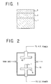
- Fig. 1 The typical layer construction of the hard multilayer film structure is shown in Fig. 1, wherein the numeral 1 stands for the substrate, 2 for the hard wear-resistant film of the titanium-containing compound (for example, TiC), and 3 for the hard carbon film containing silicon.
- the numeral 1 stands for the substrate
- 2 for the hard wear-resistant film of the titanium-containing compound (for example, TiC)
- 3 for the hard carbon film containing silicon.
- the layers 2 and 3 are formed severally by the plasma CVD technique.
- the hard wear-resistant layer 2 of the titanium-containing compound is formed of TiC or TiN, for example, and is intended to furnish the structure with resistance to wear.
- the thickness of the hard titanium-containing compound layer 2 is suitably in the range of 0.5 to 5.0 ⁇ m.
- the silicon-containing hard carbon layer 3 is vested with self-lubricating properties, resistance to wear, and resistance to heat.
- the Si content of the hard carbon layer 3 is suitably in the range of 5 to 40 atomic percent, preferably 20 to 40 atomic percent. If the Si content is less than 5 atomic percent, the hard carbon layer 3 exhibits no sufficient adhesiveness to the underlying titanium-containing compound layer. If the Si content exceeds 40 atomic percent, then the hard carbon layer 3 impairs the self-lubricating function of the structure.
- the thickness of the silicon-containing hard carbon layer 3 is suitably in the range of 0.5 to 4.0 ⁇ m.
- a method of the present invention for producing the hard multilayer film structure mentioned above includes the steps of:
- a film of a titanium-containing compound such as TiC is formed by the plasma CVD process
- the ratio of the amount of CH4 to the amount of H2 (TiCl4) as a carrier gas are set below a certain value (approximately 0.02 at 20°C, the temperature of a TiCl4 vaporizer), namely the amount of CH4 is controlled below a certain level
- the edge part of the substrate is suffered to form graphite of poor adhesiveness and the edge part is not easily coated sufficiently with TiC film especially if the substrate to be coated happens to have a three-dimensional shape.
- the film suffers from inclusion therein of a large amount of residual chlorine unless it is formed at an elevated temperature, for example in the neighborhood of 500°C.
- the titanium-containing compound film is deposited on the substrate heated to a temperature of about 400°C to about 550°C.
- the pressure within the deposition chamber is kept at a reduced pressure, preferably at the same pressure as that employed for the deposition of silicon-containing carbon layer.
- a suitable source of nitrogen such as N2 gas is additionally incorporated into the aforementioned raw gas.
- a raw gas containing tetramethyl silane or tetraethyl silane alone or in combination with hydrocarbon and/or hydrogen is employed to deposit the silicon-containing carbon layer.
- the tetramethyl silane or tetraethyl silane is a compound having four methyl groups or ethyl groups bonded to a silicon atom. Since this compound has the silicon atom coupled to carbon atoms already in the state of a raw material gas, it is characterized in that it allows ready uniform dispersion of silicon in carbon and forms graphite consisting solely of carbon bonds in the edge parts of the substrate at elevated temperatures only with great difficulty.
- the component elements of the film are mutually diffused and consequently enabled to strongly join the silicon-containing hard carbon layer to the underlying titanium-containing compound layer without requiring interposition therebetween of an intermediate layer for the purpose of enhancing the adhesiveness, such as an amorphous carbon layer containing a titanium-containing compound whose content is gradually decreased toward the surface thereof.
- the present invention is enabled by the use of tetramethyl silane or tetraethyl silane to produce a hard carbon film without formation of graphite at a pressure falling in a wide range of 0.05 to 0.5 Torr.
- the mixing ratio of carbon and silicon in the hard carbon film can be easily controlled under fixed conditions of pressure, temperature, etc.
- the frictional wear characteristics of the hard carbon film are influenced by the hydrogen content in the film.
- the frictional wear characteristics of the hard carbon film can be controlled by adjusting the hydrogen content in the hard carbon film.
- the produced film suffers from persistence therein of large residual stress if the pressure during the growth of film is low and the residual stress possibly forms a cause for separation of carbon film.
- This invention enables the residual stress in the hard carbon film to be repressed because it permits the film to be grown at such a high pressure as mentioned above.
- the hard carbon film of this invention is grown at a high temperature up to 550°C, it is stable and manifests outstanding resistance to heat under conditions of actual use involving a temperature even exceeding 400°C.
- reaction gases which are used during the doposition of the hard carbon film are invariably formed of the component elements of the film, there is no possibility of the produced hard carbon film entrapping therein such impurities as chlorine which would occur when the film is formed by using TiCl4.
- the present invention does not prohibit an intermediate carbon layer containing a titanium-containing compound with inclined content therein being interposed between the titanium-containing compound layer 2 and the silicon-containing hard carbon layer 3 shown in Fig. 1.
- This intermediate layer is formed of a hard amorphous carbon film containing the titanium-containing compound whose content is gradually decreased toward the surface thereof and serves the purpose of enhancing the adhesiveness of the hard carbon layer to the titanium-containing compound layer, as disclosed in copending U.S. application Ser. No. 861,246 of Kawamura et al. filed March 31, 1992, assigned to the same assignee as the present invention, and the corresponding German patent application No. 42 11 829.8 (Publication No. 42 11 829), the teachings thereof are hereby incorporated by reference.
- a substrate 1 of high speed tool steel [JIS (Japanese Industrial Standard) SKH51] was set in place on a DC electrode 11 disposed inside the chamber 10, and the substrate was kept at a temperature of 500°C and a discharge electrode 12 was caused to generate RF discharge under the conditions of gas flow ratio, CH4/H2 (TiCl4), of 0.02 and pressure of 0.3 Torr to deposit a TiC film 2 of a thickness of 2.0 ⁇ m on the substrate 1 as shown in Fig. 1. Thereafter, the reaction gases were switched to tetramethyl silane and hydrogen and the system was continuously operated under the conditions of substrate temperature of 500°C and pressure of 0.3 Torr to deposit a silicon-containing hard carbon film 3 in a thickness of 1 ⁇ m.
- JIS Japanese Industrial Standard
- the hard multilayer film structure obtained was not found to induce layer separation even when the deposition of film was effected under high pressure. It was found to have the multilayer film of the construction described above deposited with ample adhesiveness on the substrate. In a heating test conducted on the product, no graphitization of the carbon film proceeded at temperatures up to 550°C.
- the silicon-containing hard carbon film in the multilayer film structure according to the present invention was formed at a relatively high temperature, it prevented the otherwise possible occurrence of graphitization until a high temperature and proved itself to be highly resistance to heat.
- the present invention enables the underlying titanium-containing compound (TiC or TiN) layer to confer wear resistance and the overlying hard carbon layer containing silicon to confer self-lubricating properties and wear resistance respectively on the produced hard multilayer film structure. Moreover, these layers adhere very fast to each other and will not easily separate. Therefore, when the hard multilayer film structure according to the present invention is used as a sliding surface of a machine part which operates in the absence of lubrication, for example, even after the silicon-containing hard carbon film has been worn out, the second hard wear-resistant layer of titanium-containing compound can prevent the otherwise possible mutual adhesion of the metal surfaces by seizing.
- TiC or TiN titanium-containing compound
Landscapes
- Chemical & Material Sciences (AREA)
- Inorganic Chemistry (AREA)
- Chemical Kinetics & Catalysis (AREA)
- Engineering & Computer Science (AREA)
- Materials Engineering (AREA)
- Mechanical Engineering (AREA)
- Metallurgy (AREA)
- Organic Chemistry (AREA)
- General Chemical & Material Sciences (AREA)
- Chemical Vapour Deposition (AREA)
- Cutting Tools, Boring Holders, And Turrets (AREA)
Applications Claiming Priority (2)
| Application Number | Priority Date | Filing Date | Title |
|---|---|---|---|
| JP20504292A JPH0649645A (ja) | 1992-07-31 | 1992-07-31 | 硬質多層膜形成体およびその製造方法 |
| JP205042/92 | 1992-07-31 |
Publications (2)
| Publication Number | Publication Date |
|---|---|
| EP0585583A1 true EP0585583A1 (de) | 1994-03-09 |
| EP0585583B1 EP0585583B1 (de) | 1996-06-12 |
Family
ID=16500490
Family Applications (1)
| Application Number | Title | Priority Date | Filing Date |
|---|---|---|---|
| EP19930111483 Expired - Lifetime EP0585583B1 (de) | 1992-07-31 | 1993-07-16 | Harter, mehrlagiger Film und Verfahren zu seiner Herstellung |
Country Status (4)
| Country | Link |
|---|---|
| US (2) | US5663000A (de) |
| EP (1) | EP0585583B1 (de) |
| JP (1) | JPH0649645A (de) |
| DE (1) | DE69303127T2 (de) |
Cited By (2)
| Publication number | Priority date | Publication date | Assignee | Title |
|---|---|---|---|---|
| EP1174528A2 (de) * | 2000-07-13 | 2002-01-23 | Hitachi Tool Engineering Ltd. | Mehrlagig beschichtetes Schneidwerkzeug |
| CN113943933A (zh) * | 2020-07-16 | 2022-01-18 | 江苏菲沃泰纳米科技股份有限公司 | 多层结构的复合膜及其制备方法和产品 |
Families Citing this family (7)
| Publication number | Priority date | Publication date | Assignee | Title |
|---|---|---|---|---|
| JPH09111460A (ja) * | 1995-10-11 | 1997-04-28 | Anelva Corp | チタン系導電性薄膜の作製方法 |
| US5900289A (en) * | 1995-11-29 | 1999-05-04 | Antec Angewandte Neue Technologien Gmbh | Method of producing a colorating coating |
| JP3679882B2 (ja) * | 1997-02-07 | 2005-08-03 | 株式会社荏原製作所 | 研磨用クロスのドレッサー及びその製造方法 |
| US6360423B1 (en) | 1997-12-16 | 2002-03-26 | Clad Metals Llc | Stick resistant coating for cookware |
| US7093340B2 (en) | 1997-12-16 | 2006-08-22 | All-Clad Metalcrafters Llc | Stick resistant ceramic coating for cookware |
| JP5432457B2 (ja) * | 2008-01-28 | 2014-03-05 | パナソニック株式会社 | ダイヤモンド状炭素被膜の製造方法 |
| JP5661513B2 (ja) * | 2011-03-03 | 2015-01-28 | 東京エレクトロン株式会社 | プラズマ処理装置 |
Citations (7)
| Publication number | Priority date | Publication date | Assignee | Title |
|---|---|---|---|---|
| JPS5925973A (ja) * | 1982-08-04 | 1984-02-10 | Hitachi Metals Ltd | 多重被覆材料およびその製造法 |
| EP0193998A1 (de) * | 1985-03-07 | 1986-09-10 | Koninklijke Philips Electronics N.V. | Verfahren zur Abscheidung auf einem Substrat von einer, im wesentlichen aus Siliciumcarbid bestehenden Schicht |
| EP0229936A1 (de) * | 1985-12-17 | 1987-07-29 | Technische Universität Chemnitz | Hartstoffschichten für mechanisch und korrosiv beanspruchte Teile |
| FR2596775A1 (fr) * | 1986-04-07 | 1987-10-09 | Univ Limoges | Revetement dur multicouches elabore par depot ionique de nitrure de titane, carbonitrure de titane et i-carbone |
| JPS63286576A (ja) * | 1987-05-19 | 1988-11-24 | Idemitsu Petrochem Co Ltd | 硬質炭素膜の製造方法 |
| EP0446988A1 (de) * | 1990-03-09 | 1991-09-18 | ENIRICERCHE S.p.A. | Siliziumkarbid-Beschichtungen |
| DE4211829A1 (de) * | 1991-04-08 | 1992-11-05 | Yoshida Kogyo Kk | Artikel mit mehrlagen-hartbeschichtung und verfahren zu seiner herstellung |
Family Cites Families (15)
| Publication number | Priority date | Publication date | Assignee | Title |
|---|---|---|---|---|
| US3787223A (en) * | 1968-10-16 | 1974-01-22 | Texas Instruments Inc | Chemical vapor deposition coatings on titanium |
| IL63802A (en) * | 1981-09-11 | 1984-10-31 | Iscar Ltd | Sintered hard metal products having a multi-layer wear-resistant coating |
| DE3515919A1 (de) * | 1985-05-03 | 1986-11-06 | Fried. Krupp Gmbh, 4300 Essen | Verschleissfester beschichteter hartmetallkoerper und verfahren zu seiner herstellung |
| JPS627267A (ja) * | 1985-07-03 | 1987-01-14 | Konishiroku Photo Ind Co Ltd | 網点形成方法 |
| JPS6240375A (ja) * | 1985-08-14 | 1987-02-21 | Kanegafuchi Chem Ind Co Ltd | 硬質カ−ボン膜 |
| US4895765A (en) * | 1985-09-30 | 1990-01-23 | Union Carbide Corporation | Titanium nitride and zirconium nitride coating compositions, coated articles and methods of manufacture |
| US4686156A (en) * | 1985-10-11 | 1987-08-11 | Gte Service Corporation | Coated cemented carbide cutting tool |
| JPS63145776A (ja) * | 1987-09-12 | 1988-06-17 | Semiconductor Energy Lab Co Ltd | 被膜作成方法 |
| US5223337A (en) * | 1988-12-10 | 1993-06-29 | Fried. Krupp Gmbh | Tool produced by a plasma-activated CVD process |
| JPH02232304A (ja) * | 1989-03-06 | 1990-09-14 | Sanyo Special Steel Co Ltd | 耐食耐熱耐摩部材の製造方法およびその製品部材 |
| US5266409A (en) * | 1989-04-28 | 1993-11-30 | Digital Equipment Corporation | Hydrogenated carbon compositions |
| JP2646291B2 (ja) * | 1989-09-11 | 1997-08-27 | ユニオン・カーバイド・コーティングズ・サービセズ・テクノロジー・コーポレイション | 窒化チタン化合物の多層被覆及びその形成法 |
| US5266389A (en) * | 1989-09-29 | 1993-11-30 | Sumitomo Electric Industries, Ltd. | Surface-coated hard material for cutting tools or wear resistance tools |
| US5185211A (en) * | 1991-07-11 | 1993-02-09 | Praxair S.T. Technology, Inc. | Non-stoichiometric titanium nitride coating |
| US5249554A (en) * | 1993-01-08 | 1993-10-05 | Ford Motor Company | Powertrain component with adherent film having a graded composition |
-
1992
- 1992-07-31 JP JP20504292A patent/JPH0649645A/ja active Pending
-
1993
- 1993-07-14 US US08/090,924 patent/US5663000A/en not_active Expired - Fee Related
- 1993-07-16 EP EP19930111483 patent/EP0585583B1/de not_active Expired - Lifetime
- 1993-07-16 DE DE69303127T patent/DE69303127T2/de not_active Expired - Fee Related
-
1995
- 1995-03-07 US US08/399,641 patent/US5462775A/en not_active Expired - Lifetime
Patent Citations (7)
| Publication number | Priority date | Publication date | Assignee | Title |
|---|---|---|---|---|
| JPS5925973A (ja) * | 1982-08-04 | 1984-02-10 | Hitachi Metals Ltd | 多重被覆材料およびその製造法 |
| EP0193998A1 (de) * | 1985-03-07 | 1986-09-10 | Koninklijke Philips Electronics N.V. | Verfahren zur Abscheidung auf einem Substrat von einer, im wesentlichen aus Siliciumcarbid bestehenden Schicht |
| EP0229936A1 (de) * | 1985-12-17 | 1987-07-29 | Technische Universität Chemnitz | Hartstoffschichten für mechanisch und korrosiv beanspruchte Teile |
| FR2596775A1 (fr) * | 1986-04-07 | 1987-10-09 | Univ Limoges | Revetement dur multicouches elabore par depot ionique de nitrure de titane, carbonitrure de titane et i-carbone |
| JPS63286576A (ja) * | 1987-05-19 | 1988-11-24 | Idemitsu Petrochem Co Ltd | 硬質炭素膜の製造方法 |
| EP0446988A1 (de) * | 1990-03-09 | 1991-09-18 | ENIRICERCHE S.p.A. | Siliziumkarbid-Beschichtungen |
| DE4211829A1 (de) * | 1991-04-08 | 1992-11-05 | Yoshida Kogyo Kk | Artikel mit mehrlagen-hartbeschichtung und verfahren zu seiner herstellung |
Non-Patent Citations (3)
| Title |
|---|
| DATABASE WPI Section Ch Week 8412, 10 February 1984 Derwent World Patents Index; Class L02, AN 84-071761 * |
| DATABASE WPI Section Ch Week 8902, 24 November 1988 Derwent World Patents Index; Class E36, AN 89-011292 * |
| O. KNOTEK ET AL.: "Amorphous SiC PVD coatings", DIAMOND AND RELATED MATERIALS, vol. 2, 31 March 1993 (1993-03-31), LAUSANNE (CH), pages 528 - 530, XP000361196 * |
Cited By (4)
| Publication number | Priority date | Publication date | Assignee | Title |
|---|---|---|---|---|
| EP1174528A2 (de) * | 2000-07-13 | 2002-01-23 | Hitachi Tool Engineering Ltd. | Mehrlagig beschichtetes Schneidwerkzeug |
| EP1174528A3 (de) * | 2000-07-13 | 2004-05-06 | Hitachi Tool Engineering Ltd. | Mehrlagig beschichtetes Schneidwerkzeug |
| CN113943933A (zh) * | 2020-07-16 | 2022-01-18 | 江苏菲沃泰纳米科技股份有限公司 | 多层结构的复合膜及其制备方法和产品 |
| CN113943933B (zh) * | 2020-07-16 | 2023-09-29 | 江苏菲沃泰纳米科技股份有限公司 | 多层结构的复合膜及其制备方法和产品 |
Also Published As
| Publication number | Publication date |
|---|---|
| DE69303127T2 (de) | 1997-01-23 |
| US5663000A (en) | 1997-09-02 |
| DE69303127D1 (de) | 1996-07-18 |
| EP0585583B1 (de) | 1996-06-12 |
| US5462775A (en) | 1995-10-31 |
| JPH0649645A (ja) | 1994-02-22 |
Similar Documents
| Publication | Publication Date | Title |
|---|---|---|
| US5260107A (en) | Plasma chemical vapor deposition process for producing a hard multilayer coated product | |
| EP0523021B1 (de) | Verfahren zur Herstellung eines mit Aluminiumoxyd beschichteten gesinterten Formkörper | |
| EP0685572B1 (de) | Beschichtete Klinge aus Hartmetallegierung | |
| EP0816531B1 (de) | Aluminiumoxid-beschichtetes Werkzeug und Verfahren zu seiner Herstellung | |
| US4269899A (en) | Surface hafnium-titanium carbide coated hard alloy and method | |
| US6689450B2 (en) | Enhanced Al2O3-Ti(C,N) multi-coating deposited at low temperature | |
| EP0085240B1 (de) | Mehrlagig beschichtete Schneidwerkzeuge und Verfahren zur Herstellung | |
| US5985427A (en) | Coated carbide alloy cutting member exhibiting excellent resistance against chipping | |
| EP0653499A1 (de) | Beschichtetes schneidwerkzeug und verfahren zu dessen herstellung | |
| US5436071A (en) | Cermet cutting tool and process for producing the same | |
| EP0709484A1 (de) | Beschichtete Klinge aus Sinterkarbid auf Wolframkarbidbasis | |
| EP0585583B1 (de) | Harter, mehrlagiger Film und Verfahren zu seiner Herstellung | |
| JP3052586B2 (ja) | 耐チッピング性にすぐれた表面被覆炭化タングステン基超硬合金製切削工具 | |
| US6632514B1 (en) | Coated cutting insert for milling and turning applications | |
| JP2867803B2 (ja) | 耐チッピング性にすぐれた表面被覆炭化タングステン基超硬合金製切削工具 | |
| NL8500645A (nl) | Werkwijze voor het afzetten van een laag, die in hoofdzaak uit siliciumcarbide bestaat op een substraat. | |
| US6228483B1 (en) | Abrasion resistant coated articles | |
| EP0447556B1 (de) | Oberflächenbeschichteter hartwerkstoff mit ausgezeichneter verschleissfestigkeit | |
| JPH02311202A (ja) | 被覆切削工具 | |
| JP2927181B2 (ja) | 硬質被覆層がすぐれた層間密着性を有する表面被覆炭化タングステン基超硬合金製切削工具 | |
| Cerio et al. | Machining of abrasive materials with diamond-coated tungsten carbide inserts | |
| JP3109272B2 (ja) | 耐欠損性および耐摩耗性にすぐれた表面被覆炭窒化チタン基サーメット製切削工具 | |
| JP3265974B2 (ja) | 耐チッピング性のすぐれた表面被覆超硬合金製切削工具の製造法 | |
| JPH08187604A (ja) | 硬質被覆層がすぐれた層間密着性を有する表面被覆炭化タングステン基超硬合金製切削工具 | |
| JPH04231468A (ja) | 表面被覆TiCN基サーメット |
Legal Events
| Date | Code | Title | Description |
|---|---|---|---|
| PUAI | Public reference made under article 153(3) epc to a published international application that has entered the european phase |
Free format text: ORIGINAL CODE: 0009012 |
|
| AK | Designated contracting states |
Kind code of ref document: A1 Designated state(s): DE FR GB IT SE |
|
| 17P | Request for examination filed |
Effective date: 19940711 |
|
| RAP1 | Party data changed (applicant data changed or rights of an application transferred) |
Owner name: YKK CORPORATION |
|
| 17Q | First examination report despatched |
Effective date: 19950424 |
|
| GRAH | Despatch of communication of intention to grant a patent |
Free format text: ORIGINAL CODE: EPIDOS IGRA |
|
| GRAH | Despatch of communication of intention to grant a patent |
Free format text: ORIGINAL CODE: EPIDOS IGRA |
|
| GRAA | (expected) grant |
Free format text: ORIGINAL CODE: 0009210 |
|
| AK | Designated contracting states |
Kind code of ref document: B1 Designated state(s): DE FR GB IT SE |
|
| ITF | It: translation for a ep patent filed | ||
| ET | Fr: translation filed | ||
| REF | Corresponds to: |
Ref document number: 69303127 Country of ref document: DE Date of ref document: 19960718 |
|
| PLBE | No opposition filed within time limit |
Free format text: ORIGINAL CODE: 0009261 |
|
| STAA | Information on the status of an ep patent application or granted ep patent |
Free format text: STATUS: NO OPPOSITION FILED WITHIN TIME LIMIT |
|
| 26N | No opposition filed | ||
| REG | Reference to a national code |
Ref country code: GB Ref legal event code: IF02 |
|
| PGFP | Annual fee paid to national office [announced via postgrant information from national office to epo] |
Ref country code: DE Payment date: 20070712 Year of fee payment: 15 |
|
| PGFP | Annual fee paid to national office [announced via postgrant information from national office to epo] |
Ref country code: GB Payment date: 20070711 Year of fee payment: 15 |
|
| PGFP | Annual fee paid to national office [announced via postgrant information from national office to epo] |
Ref country code: SE Payment date: 20070704 Year of fee payment: 15 Ref country code: IT Payment date: 20070727 Year of fee payment: 15 |
|
| PGFP | Annual fee paid to national office [announced via postgrant information from national office to epo] |
Ref country code: FR Payment date: 20070710 Year of fee payment: 15 |
|
| EUG | Se: european patent has lapsed | ||
| GBPC | Gb: european patent ceased through non-payment of renewal fee |
Effective date: 20080716 |
|
| PG25 | Lapsed in a contracting state [announced via postgrant information from national office to epo] |
Ref country code: DE Free format text: LAPSE BECAUSE OF NON-PAYMENT OF DUE FEES Effective date: 20090203 |
|
| REG | Reference to a national code |
Ref country code: FR Ref legal event code: ST Effective date: 20090331 |
|
| PG25 | Lapsed in a contracting state [announced via postgrant information from national office to epo] |
Ref country code: GB Free format text: LAPSE BECAUSE OF NON-PAYMENT OF DUE FEES Effective date: 20080716 |
|
| PG25 | Lapsed in a contracting state [announced via postgrant information from national office to epo] |
Ref country code: IT Free format text: LAPSE BECAUSE OF NON-PAYMENT OF DUE FEES Effective date: 20080716 Ref country code: FR Free format text: LAPSE BECAUSE OF NON-PAYMENT OF DUE FEES Effective date: 20080731 |
|
| PG25 | Lapsed in a contracting state [announced via postgrant information from national office to epo] |
Ref country code: SE Free format text: LAPSE BECAUSE OF NON-PAYMENT OF DUE FEES Effective date: 20080717 |