EP0582397A2 - Matériel en diamant CVD pour détecteur de radiation et procédé pour fabriquer celui-ci - Google Patents
Matériel en diamant CVD pour détecteur de radiation et procédé pour fabriquer celui-ci Download PDFInfo
- Publication number
- EP0582397A2 EP0582397A2 EP93305615A EP93305615A EP0582397A2 EP 0582397 A2 EP0582397 A2 EP 0582397A2 EP 93305615 A EP93305615 A EP 93305615A EP 93305615 A EP93305615 A EP 93305615A EP 0582397 A2 EP0582397 A2 EP 0582397A2
- Authority
- EP
- European Patent Office
- Prior art keywords
- diamond
- microns
- diamond film
- conductive strips
- film
- Prior art date
- Legal status (The legal status is an assumption and is not a legal conclusion. Google has not performed a legal analysis and makes no representation as to the accuracy of the status listed.)
- Withdrawn
Links
Images


Classifications
-
- C—CHEMISTRY; METALLURGY
- C23—COATING METALLIC MATERIAL; COATING MATERIAL WITH METALLIC MATERIAL; CHEMICAL SURFACE TREATMENT; DIFFUSION TREATMENT OF METALLIC MATERIAL; COATING BY VACUUM EVAPORATION, BY SPUTTERING, BY ION IMPLANTATION OR BY CHEMICAL VAPOUR DEPOSITION, IN GENERAL; INHIBITING CORROSION OF METALLIC MATERIAL OR INCRUSTATION IN GENERAL
- C23C—COATING METALLIC MATERIAL; COATING MATERIAL WITH METALLIC MATERIAL; SURFACE TREATMENT OF METALLIC MATERIAL BY DIFFUSION INTO THE SURFACE, BY CHEMICAL CONVERSION OR SUBSTITUTION; COATING BY VACUUM EVAPORATION, BY SPUTTERING, BY ION IMPLANTATION OR BY CHEMICAL VAPOUR DEPOSITION, IN GENERAL
- C23C16/00—Chemical coating by decomposition of gaseous compounds, without leaving reaction products of surface material in the coating, i.e. chemical vapour deposition [CVD] processes
- C23C16/22—Chemical coating by decomposition of gaseous compounds, without leaving reaction products of surface material in the coating, i.e. chemical vapour deposition [CVD] processes characterised by the deposition of inorganic material, other than metallic material
- C23C16/26—Deposition of carbon only
- C23C16/27—Diamond only
- C23C16/274—Diamond only using microwave discharges
-
- C—CHEMISTRY; METALLURGY
- C23—COATING METALLIC MATERIAL; COATING MATERIAL WITH METALLIC MATERIAL; CHEMICAL SURFACE TREATMENT; DIFFUSION TREATMENT OF METALLIC MATERIAL; COATING BY VACUUM EVAPORATION, BY SPUTTERING, BY ION IMPLANTATION OR BY CHEMICAL VAPOUR DEPOSITION, IN GENERAL; INHIBITING CORROSION OF METALLIC MATERIAL OR INCRUSTATION IN GENERAL
- C23C—COATING METALLIC MATERIAL; COATING MATERIAL WITH METALLIC MATERIAL; SURFACE TREATMENT OF METALLIC MATERIAL BY DIFFUSION INTO THE SURFACE, BY CHEMICAL CONVERSION OR SUBSTITUTION; COATING BY VACUUM EVAPORATION, BY SPUTTERING, BY ION IMPLANTATION OR BY CHEMICAL VAPOUR DEPOSITION, IN GENERAL
- C23C16/00—Chemical coating by decomposition of gaseous compounds, without leaving reaction products of surface material in the coating, i.e. chemical vapour deposition [CVD] processes
- C23C16/22—Chemical coating by decomposition of gaseous compounds, without leaving reaction products of surface material in the coating, i.e. chemical vapour deposition [CVD] processes characterised by the deposition of inorganic material, other than metallic material
- C23C16/26—Deposition of carbon only
- C23C16/27—Diamond only
- C23C16/277—Diamond only using other elements in the gas phase besides carbon and hydrogen; using other elements besides carbon, hydrogen and oxygen in case of use of combustion torches; using other elements besides carbon, hydrogen and inert gas in case of use of plasma jets
-
- C—CHEMISTRY; METALLURGY
- C23—COATING METALLIC MATERIAL; COATING MATERIAL WITH METALLIC MATERIAL; CHEMICAL SURFACE TREATMENT; DIFFUSION TREATMENT OF METALLIC MATERIAL; COATING BY VACUUM EVAPORATION, BY SPUTTERING, BY ION IMPLANTATION OR BY CHEMICAL VAPOUR DEPOSITION, IN GENERAL; INHIBITING CORROSION OF METALLIC MATERIAL OR INCRUSTATION IN GENERAL
- C23C—COATING METALLIC MATERIAL; COATING MATERIAL WITH METALLIC MATERIAL; SURFACE TREATMENT OF METALLIC MATERIAL BY DIFFUSION INTO THE SURFACE, BY CHEMICAL CONVERSION OR SUBSTITUTION; COATING BY VACUUM EVAPORATION, BY SPUTTERING, BY ION IMPLANTATION OR BY CHEMICAL VAPOUR DEPOSITION, IN GENERAL
- C23C16/00—Chemical coating by decomposition of gaseous compounds, without leaving reaction products of surface material in the coating, i.e. chemical vapour deposition [CVD] processes
- C23C16/44—Chemical coating by decomposition of gaseous compounds, without leaving reaction products of surface material in the coating, i.e. chemical vapour deposition [CVD] processes characterised by the method of coating
- C23C16/50—Chemical coating by decomposition of gaseous compounds, without leaving reaction products of surface material in the coating, i.e. chemical vapour deposition [CVD] processes characterised by the method of coating using electric discharges
- C23C16/511—Chemical coating by decomposition of gaseous compounds, without leaving reaction products of surface material in the coating, i.e. chemical vapour deposition [CVD] processes characterised by the method of coating using electric discharges using microwave discharges
-
- G—PHYSICS
- G01—MEASURING; TESTING
- G01T—MEASUREMENT OF NUCLEAR OR X-RADIATION
- G01T1/00—Measuring X-radiation, gamma radiation, corpuscular radiation, or cosmic radiation
- G01T1/16—Measuring radiation intensity
- G01T1/20—Measuring radiation intensity with scintillation detectors
- G01T1/202—Measuring radiation intensity with scintillation detectors the detector being a crystal
-
- G—PHYSICS
- G01—MEASURING; TESTING
- G01T—MEASUREMENT OF NUCLEAR OR X-RADIATION
- G01T1/00—Measuring X-radiation, gamma radiation, corpuscular radiation, or cosmic radiation
- G01T1/16—Measuring radiation intensity
- G01T1/26—Measuring radiation intensity with resistance detectors
Definitions
- the present invention relates to chemical vapor deposited diamond materials. More particularly, the present invention relates to CVD diamond materials suitable for making detectors for detecting radiation, such as x-rays, gamma rays, ultraviolet, high energy particles, and the like, and to processes for fabricating such materials.
- Materials comprising doped silicon junctions have been used as radiation detectors.
- the closest known prior art is the use of natural diamond for detectors for detecting radiation, such as ultraviolet, x-rays, gamma rays, high energy particles, and the like.
- natural diamond did not find wide spread use as a radiation detector due to several disadvantages associated therewith.
- Kozlov et al. have extensively studied natural diamond as a radiation detector. They measured the response of natural diamond to alpha particles and determined the energy resolution. In addition, they found that the carrier lifetime is a function of the nitrogen impurity concentration. For diamond with a nitrogen concentration less than 1019/cm3, the measured lifetimes were greater than 1 nsec. The resistance of the diamond detectors to radiation damage caused by neutrons was also measured.
- a technology for fabricating synthetic diamond materials by chemical vapor deposition (CVD) has recently been developed. This technology has the potential for solving these problems and allows diamond to be grown in large sheets at a reasonable cost. Although it has been theoretically feasible to fabricate commercially-acceptable radiation detectors from synthetic CVD diamond materials to avoid the inherent problems associated with natural diamond, to date there have been no successful attempts at producing CVD diamond radiation detectors having commercially-useful characteristics.
- CVD diamond radiation detectors would provide a unique opportunity for investigating a new unexplored energy region in high-energy physics.
- Experiments using such detectors in tracking detectors and calorimeters could be capable of definitive searches for the Higgs, supersymmetry, technicolor, compositeness, etc., which so far have eluded experimental detection, as well as the ability to recognize unanticipated phenomena.
- the signatures for new physics include the production of high transverse momentum leptons, jets and missing energy.
- Higgs searches require lepton and jet reconstruction while supersymmetry and technicolor searches require finely segmented hermetic calorimetry to determine the missing energy.
- a further object of the invention is to provide a commercially-acceptable radiation detector incorporating a CVD diamond detector element.
- Yet another object of the invention is to provide a fabrication process for a CVD diamond material having properties which make it suitable for use as a radiation detector element.
- the present invention comprises a radiation detector based on the novel use of diamond technology to survive in a high radiation environment and methods for fabricating such detectors.
- the diamond detectors of the present invention detect radiation,which is capable of producing free current carriers in diamond.
- radiation typically, such radiation includes light and energetic particles which have energies greater than 5.45 eV.
- CVD diamond films useful for radiation detectors comprise diamond films having an average grain size of at least 7 microns, and preferably at least 15 microns.
- the grain size of the best material produced to date has been 15 microns.
- the films of the present invention are typically grown on substrates having deposited diamond films of a similar grain size.
- the diamond materials of the present inventions preferably contain no more than minimal amounts of nitrogen.
- the diamond films of the present invention have a carrier mobility of at least 1,000 cm2/V-sec, a carrier lifetime of at least 100 psec and less than 200 nsec, yielding a collection distance of at least 10 microns at an electric field strength of 104 V/cm.
- the diamond films of the present invention have a resistivity of at least 1010 ⁇ -cm. Measurements of the surface layer by time resolved photoconductivity indicate combined mobilities as high as 4000-5000 cm2/V-sec and carrier lifetimes of as high as 1500 picoseconds.
- a surface radiation detector comprises a diamond film grown according to the teachings of the present invention.
- the diamond film should have a minimum thickness of about 1 microns and an area of at least about 1 mm2. The maximum thickness of such a diamond film is relatively unimportant, since only the surface layer is utilized.
- a set of first parallel conductive strips and a second set of parallel conductive strips, offset from and spaced apart from the first set of parallel strips, are disposed on the surface of the diamond film.
- the conductive strips preferably comprising a deposited titanium/gold film.
- a plurality of active detector areas comprises the regions between pairs of first and second conductive strips.
- a plurality of parallel conductive strips, preferably comprising a titanium/gold film layer are disposed on the surface of the diamond film and spaced apart by a selected active region distance.
- Alternating ones of the conductive strips are electrically connected to one another, preferably by one of two regions of the titanium/gold film layer disposed adjacent to the periphery of the measuring area of the film and running orthogonal to and in contact with alternating ones of the conductive strips to form an interlaced comb-like pattern.
- a bulk radiation detector comprises a block of diamond film having an upper surface and a lower surface, and having a thickness of between about 10 microns and several hundred microns.
- an upper layer and a lower layer of conductive film preferably comprising a deposited titanium/gold layer, are respectively disposed over an area of about 1 mm2 or larger on each of the upper and lower surfaces of the block of diamond film.
- the upper and lower film layers are aligned to one another.
- a layer of conductive film, preferably comprising a deposited titanium/gold layer is disposed over an area of about 1 mm2 or larger on one of the upper and lower surfaces.
- a plurality of spaced apart parallel conductive strips are disposed on the other one of the upper and lower surfaces of the block.
- a chemical-vapor-deposition method for producing diamond materials suitable for use as radiation detectors is disclosed.
- the diamond material of the present invention is grown on a suitable substrate material.
- Appropriate substrates include large grain polycrystalline diamond, single crystal diamond, diamond particulate composites and other non-diamond substrates that allow for large grain growth.
- detector-grade diamond can be grown using microwave plasma CVD techniques.
- Diamond materials according to the present invention have been successfully grown in a NIRIM-style microwave plasma CVD reactor having a reactor chamber volume of about 300 in3.
- Microwave energy of 2.45 GHz at a power level of between about 1,400 to 1,900 watts is introduced into the reactor chamber to create a plasma in the region of a substrate holder and achieve a substrate temperature of between about 800-1,000°C.
- the reaction may be carried out in an atmosphere of hydrogen, methane, and carbon monoxide.
- Detector grade diamond has been grown using gas flow rates of 300 sccm of hydrogen, 3 sccm of methane and 4.5 sccm of carbon monoxide at pressures from 90-100 Torr and substrate temperatures of 800-1000° C.
- FIG. 1 is a photomicrograph of CVD diamond material produced according to the present invention.
- FIG. 2 is a diagram of a top view of a surface radiation detector according to a first embodiment of the invention.
- FIG. 3 is a diagram of a top view of a surface radiation detector according to a second embodiment of the invention.
- FIG. 4 is a diagram of a cross section of a bulk radiation detector according to a first embodiment of the invention.
- FIG. 5 is a diagram of a cross section of a bulk radiation detector according to a second embodiment of the invention.
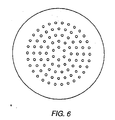
- FIG. 6 is a face view of a showerhead gas delivery apparatus suitable for use in the present invention.
- a novel CVD diamond material and radiation detectors made from the CVD diamond material are disclosed.
- the radiation detectors of the present invention can be made in larger dimensions -and at a lower cost than natural diamond detectors.
- the CVD diamond materials of the present invention have a major advantage over other suitable detector materials since it has the highest inherent resistance to radiation damage. In applications where a high total radiation dose can be contemplated, CVD diamond radiation detectors enable a large reduction in detector size compared to other solid-state detectors.
- the CVD diamond materials of the present invention are also an obvious choice as an ultraviolet detector due to their large band gap (i.e., 5.5 eV).
- Detector-grade diamond must have minimum electronic transport properties for the detector to function properly.
- CVD diamond By controlling CVD growth chemistry and grain size during growth, CVD diamond with the appropriate electronic properties can be fabricated. It has been found that CVD diamond material of the present invention can be grown with mobilities larger than and other pertinent properties better than those found in other CVD diamond and in natural diamond materials. The CVD diamond material of the present invention have carrier lifetimes comparable to that of natural diamond. The fabrication of this superior diamond material may be accomplished using the combination of large grain size and deposition chemistry disclosed herein.
- CVD diamond films suitable for use as surface radiation detectors have a minimum thickness of about 1 micron. Since only the upper surface is utilized in such a detector, the upper thickness limit is based on practical process-time considerations.
- CVD diamond films suitable for use as bulk radiation detectors have a thickness of from between about 10 microns to several hundreds of microns depending on the type of radiation to be measured and the desired response speed. In both instances, these films have an average grain size of at least 7 microns and preferably around 15 microns, and contain minimal hydrogen.
- the CVD diamond films of the present invention have advantageous electrical properties which make them more suitable for use as radiation detectors than other CVD diamond films.
- the CVD diamond films of the present invention have a resistivity of at least 1010 ⁇ -cm, a carrier mobility of at least 1,000 cm2/V-sec, a carrier lifetime of at least 100 psec and less than 200 nsec, yielding a collection distance of at least 10 microns at an electric field strength of 104 V/cm.
- FIG. 1 is a photomicrograph of a sample of CVD diamond material suitable for radiation detectors according to the present invention.
- a surface radiation detector comprises a diamond film grown according to the teachings of the present invention.
- the diamond film should have a minimum thickness of about 1 micron and an area of about 1 mm2 or larger.
- the maximum thickness of the diamond film for use as a surface detector is relatively unimportant since only the top surface of the film is utilized.
- a first embodiment of a surface radiation detector 10 comprises a CVD diamond film 12 grown according to the present invention.
- a plurality of first conductive strips 14a, 14b, and 14c, offset from a plurality of second conductive strips 16a, 16b, and 16c, are disposed on the detecting surface of the diamond film 12.
- the conductive strips may preferably comprise a titanium/gold film.
- a plurality of active detector areas comprises the regions 18a, 18b, and 18c located between pairs of first and second conductive strips.
- strips 14a and 16a may be 1 mm wide and may be offset from one another by spaces 18a and 18b of about 1mm.
- the CVD diamond film is prepared by removing any non-electronic grade diamond or other material from the areas to be metallized for the active device. This may be accomplished using conventional materials processing etch steps.
- the prepared active surface of the detector is metallized with an appropriate metal pattern.
- a set of first parallel conductive strips and a second set of parallel conductive strips, offset from and spaced apart from the first set of parallel strips, are disposed on the surface of the diamond film.
- the conductive strips preferably comprising a deposited titanium film having a thickness of about 500 ⁇ followed by gold film having a thickness of about 10,000 ⁇ or a titanium film having a thickness of about 500 ⁇ , or a similar metal system. Electrical leads may be bonded to the metal films using conventional semiconductor processing techniques.
- the three separate detector devices depicted in FIG. 2 could be either further diced into individual detectors or may be used as an array.
- a second embodiment of a surface detector is shown in top view in FIG. 3.
- the surface radiation detector 20 of the embodiment of FIG. 2 comprises a CVD diamond film 22 grown according to the present invention.
- a plurality of first conductive strips 24a, 24b, and 24c, interleaved with a plurality of second conductive strips 26a, 26b, and 26c, are disposed on the detecting surface of the diamond film 22.
- Strips 24a-24c are joined at the periphery of the detector area by orthogonally disposed contiguous strip 24d and strips 26a-26c are joined at the periphery of the detector area by orthogonally disposed contiguous strip 26d .
- a plurality of active detector areas comprises the regions located between pairs of first and second conductive strips.
- strips 24a and 26a may be about 5 microns wide and may be separated from one another by about micron.
- a CVD diamond film grown according to the present invention is prepared, as in the first embodiment, by removing any non-electronic grade diamond or other material from the areas to be metallized for the active device.
- a plurality of parallel conductive strips preferably comprising a titanium/gold film layer, are disposed on the surface of the diamond film and spaced apart by a selected active region distance. Alternating ones of the conductive strips are electrically connected to one another, preferably by one of two regions of the titanium/gold film layer disposed adjacent to the periphery of the measuring area of the film and running orthogonal to and in contact with alternating ones of the conductive strips to form an interlaced comb-like pattern.
- Detector 30 comprises a block 32 of diamond film having an upper surface 34 and a lower surface 36, and has a thickness of between about 10 microns and several hundred microns, depending on the application in which the detector will be used.
- An upper layer of conductive film 38 preferably a titanium/gold film as described herein, is disposed on upper surface 34 of block 32, and a lower layer of conductive film 40 is disposed on lower surface 36 of block 32.
- the embodiment of FIG. 4 may be fabricated by a process in which non-electronic grade CVD diamond material is first removed from the surface of the already-grown bulk diamond film.
- This step may include removal of the silicon, molybdenum, or CVD diamond substrate layer prior to metallization. This step is performed using conventional materials-processing etch steps.
- the upper and lower layers 38 and 40 of conductive film are respectively disposed over an area of about 1 mm2 or larger on each of the upper and lower surfaces of the block of diamond film.
- the upper and lower metal film layers are aligned to one another.
- FIG. 5 a cross sectional view of a second embodiment of a bulk detector 50 according to the present invention is presented.
- a layer of conductive film 40 preferably comprising a deposited titanium/gold layer, is disposed over an area of about 1 mm2 or larger on the lower surface 36 of block 32.
- a plurality of spaced-apart parallel conductive strips 52a-52e are shown- disposed on the upper surface of the block 32. Strips 52a-52e may be formed by etching a conductive layer such as layer 38 of FIG. 4 using conventional techniques.
- the embodiment of FIG. 5 comprises five separate detectors sharing common lower conductive layer 40 between them.
- a chemical-vapor-deposition method for producing diamond materials suitable for use as radiation detectors according to the present invention.
- the diamond material of the present invention is grown on a suitable substrate material.
- Appropriate substrates include large grain polycrystalline diamond, single crystal diamond, diamond particulate composites and other non-diamond substrates that allow for large grain growth.
- appropriate substrates include large-grain polycrystalline diamond, single crystal diamond, diamond particulate composites such as diamond-silicon carbide, diamond-diamond, and diamond-boron nitride, and other non-diamond substrates that allow for large grain growth, such as silicon and molybdenum.
- Diamond-diamond, and diamond-non-diamond composite substrates suitable for use in the present invention may be fabricated by utilizing the methods taught in co-pending application serial No. 07/704,997, filed May 24, 1991, and assigned to the same assignee as the present invention. This patent application is expressly incorporated herein by reference. Silicon and molybdenum substrates may be prepared by diamond polishing as is known in the art.
- detector-grade diamond can be grown on the disclosed substrates in a microwave plasma CVD system.
- Diamond materials suitable for use as radiation detectors according to the present invention have been successfully grown in a NIRIM style reactor.
- the CVD reactor used in the present invention should employ only quartz and molybdenum fixtures, and should employ only molybdenum components in the hot regions of the reactor, and should be free of graphite fixtures and other graphite contamination.
- Such a reactor actually used to grow films according to the present invention has a reactor-chamber volume of about 300 in3 and may preferably be equipped with a gas delivery system employing a showerhead fixture as shown in FIG. 6.
- the showerhead has a generally circular delivery face having a diameter of about 3.5 inches.
- the delivery face includes a plurality of gas delivery holes formed therethrough. The holes each have a diameter of about 0.020 inch and are equally spaced in a pattern comprising five concentric circles.
- a first inner circle having a diameter of about 0.5 inch includes 6 holes; a second circle having a diameter of about 1.0 inch includes 12 holes; a third circle having a diameter of about 1.5 inch includes 18 holes; a fourth circle having a diameter of about 2.0 inch includes 24 holes; a fifth circle having a diameter of about 2.5 inch includes 30 holes.
- the showerhead is positioned in the chamber at 3.5 cm to 5 cm above the substrate.
- Microwave energy of 2.45 GHz at a power level of between about 1,400 to 1,900 watts is introduced into the reaction chamber using conventional waveguides to create a plasma in the region of a substrate holder and achieve a substrate temperature of between about 800-1,000°C as measured by a dual-frequency optical pyrometer.
- the reaction may be carried out in an atmosphere of 300 sccm of hydrogen, 3 sccm of methane and 4.5 sccm of carbon monoxide at pressures from 90-100 Torr and substrate temperatures of 800-1000° C.
- gas flow rates may be adjusted for different-sized reaction chambers.
- the present invention allows for the fabrication and production of CVD diamond detectors.
- Diamond detectors can be utilized in a number of applications including, but not confined to radiation-detectors useful for high-energy physics applications and other similar high energy applications, radiation sensors for the medical community, detectors for commercial x-ray inspection of critical components, ultraviolet detectors for commercial analytical instruments and high energy physics experiments.
- CVD diamond detectors used in all of these areas will provide improved reliability and radiation tolerance of current solid state detectors. Due to the nature of CVD diamond films, these detectors can easily be fabricated in large dimensions and for a lower cost than natural diamond detectors.
- the radiation detectors of the present invention can base key sections of tracking and calorimetry on diamond technology in high-energy physics experiments. These include a diamond charged particle tracking chamber (diamond tracker), diamond electromagnetic calorimeter, and diamond-tungsten hadron calorimeter all of which will reside inside a 5 Tesla magnetic volume.
- Using the detectors of the present invention allows operation at luminosities above 1034 cm ⁇ 2s ⁇ 1 in a hadron collider. Moreover, limiting the number of distinct elements in a compact detector should keep the final design simple and economical.
- a few hundred volts are applied across a layer of diamond a few hundred microns thick.
- atoms at the crystal lattice sites are ionized, promoting electrons into the conduction band and leaving holes in the valence band.
- These charges are free to move about the crystal and drift across the layer in response to the applied electric field producing a signal pulse which can be preamplified and further processed into a detection signal.
Landscapes
- Chemical & Material Sciences (AREA)
- Engineering & Computer Science (AREA)
- Physics & Mathematics (AREA)
- Mechanical Engineering (AREA)
- Organic Chemistry (AREA)
- Metallurgy (AREA)
- General Chemical & Material Sciences (AREA)
- Chemical Kinetics & Catalysis (AREA)
- Materials Engineering (AREA)
- Inorganic Chemistry (AREA)
- Plasma & Fusion (AREA)
- Health & Medical Sciences (AREA)
- Life Sciences & Earth Sciences (AREA)
- General Physics & Mathematics (AREA)
- High Energy & Nuclear Physics (AREA)
- Molecular Biology (AREA)
- Spectroscopy & Molecular Physics (AREA)
- Combustion & Propulsion (AREA)
- Crystallography & Structural Chemistry (AREA)
- Measurement Of Radiation (AREA)
Applications Claiming Priority (2)
| Application Number | Priority Date | Filing Date | Title |
|---|---|---|---|
| US92620892A | 1992-08-05 | 1992-08-05 | |
| US926208 | 1992-08-05 |
Publications (2)
| Publication Number | Publication Date |
|---|---|
| EP0582397A2 true EP0582397A2 (fr) | 1994-02-09 |
| EP0582397A3 EP0582397A3 (fr) | 1995-01-25 |
Family
ID=25452895
Family Applications (1)
| Application Number | Title | Priority Date | Filing Date |
|---|---|---|---|
| EP93305615A Withdrawn EP0582397A3 (fr) | 1992-08-05 | 1993-07-16 | Matériel en diamant CVD pour détecteur de radiation et procédé pour fabriquer celui-ci. |
Country Status (1)
| Country | Link |
|---|---|
| EP (1) | EP0582397A3 (fr) |
Cited By (19)
| Publication number | Priority date | Publication date | Assignee | Title |
|---|---|---|---|---|
| US5773830A (en) * | 1993-07-20 | 1998-06-30 | Saint-Gobain/Norton Industrial Ceramics Corp. | CVD diamond radiation detector |
| EP1065732A1 (fr) * | 1999-06-30 | 2001-01-03 | Siemens Medical Systems, Inc. | Une structure photoconductrice interdigitée pour une détection directe de rayons X |
| WO2001069285A1 (fr) * | 2000-03-15 | 2001-09-20 | De Beers Industrial Diamonds (Proprietary) Limited | Detecteur de rayonnements a diamant |
| WO2001096633A1 (fr) * | 2000-06-15 | 2001-12-20 | Element Six (Pty) Ltd | Diamant monocristallin prepare par depot chimique en phase vapeur (cvd) |
| US6858080B2 (en) | 1998-05-15 | 2005-02-22 | Apollo Diamond, Inc. | Tunable CVD diamond structures |
| US7128974B2 (en) * | 2000-06-15 | 2006-10-31 | Geoffrey Alan Scarsbrook | Thick single crystal diamond layer method for making it and gemstones produced from the layer |
| US7201886B2 (en) | 1998-05-15 | 2007-04-10 | Apollo Diamond, Inc. | Single crystal diamond tool |
| US7662441B2 (en) | 2003-01-10 | 2010-02-16 | Centre National De La Recherche Scientifique - Cnrs | High-speed diamond growth using a microwave plasma in pulsed mode |
| WO2012084661A1 (fr) * | 2010-12-23 | 2012-06-28 | Element Six Limited | Réacteur à plasma à micro-ondes pour fabriquer un matériau de diamant synthétique |
| WO2012084656A1 (fr) * | 2010-12-23 | 2012-06-28 | Element Six Limited | Dopage contrôlé de matériau de diamant synthétique |
| US8591856B2 (en) | 1998-05-15 | 2013-11-26 | SCIO Diamond Technology Corporation | Single crystal diamond electrochemical electrode |
| US8859058B2 (en) | 2010-12-23 | 2014-10-14 | Element Six Limited | Microwave plasma reactors and substrates for synthetic diamond manufacture |
| US8955456B2 (en) | 2010-12-23 | 2015-02-17 | Element Six Limited | Microwave plasma reactor for manufacturing synthetic diamond material |
| US9142389B2 (en) | 2010-12-23 | 2015-09-22 | Element Six Technologies Limited | Microwave power delivery system for plasma reactors |
| US9317811B2 (en) | 2008-07-23 | 2016-04-19 | Element Six Technologies Limited | Diamond material |
| US9410242B2 (en) | 2010-12-23 | 2016-08-09 | Element Six Technologies Limited | Microwave plasma reactor for manufacturing synthetic diamond material |
| US9416005B2 (en) | 2008-07-23 | 2016-08-16 | Element Six Technologies Limited | Solid state material |
| US10403477B2 (en) | 2010-12-23 | 2019-09-03 | Element Six Technologies Limited | Microwave plasma reactor for manufacturing synthetic diamond material |
| US10954607B1 (en) | 2019-10-22 | 2021-03-23 | Euclid Techlabs, Llc | High-efficiency transmission-mode diamond scintillator for quantitative characterization of X-ray beams |
Citations (3)
| Publication number | Priority date | Publication date | Assignee | Title |
|---|---|---|---|---|
| EP0392461A2 (fr) * | 1989-04-12 | 1990-10-17 | Sumitomo Electric Industries, Ltd. | Thermistance préparé à partir de diamant |
| US5079425A (en) * | 1990-01-10 | 1992-01-07 | Sumitomo Electric Industries, Ltd. | Radiation detecting element |
| US5099788A (en) * | 1989-07-05 | 1992-03-31 | Nippon Soken, Inc. | Method and apparatus for forming a diamond film |
-
1993
- 1993-07-16 EP EP93305615A patent/EP0582397A3/fr not_active Withdrawn
Patent Citations (3)
| Publication number | Priority date | Publication date | Assignee | Title |
|---|---|---|---|---|
| EP0392461A2 (fr) * | 1989-04-12 | 1990-10-17 | Sumitomo Electric Industries, Ltd. | Thermistance préparé à partir de diamant |
| US5099788A (en) * | 1989-07-05 | 1992-03-31 | Nippon Soken, Inc. | Method and apparatus for forming a diamond film |
| US5079425A (en) * | 1990-01-10 | 1992-01-07 | Sumitomo Electric Industries, Ltd. | Radiation detecting element |
Cited By (48)
| Publication number | Priority date | Publication date | Assignee | Title |
|---|---|---|---|---|
| US5773830A (en) * | 1993-07-20 | 1998-06-30 | Saint-Gobain/Norton Industrial Ceramics Corp. | CVD diamond radiation detector |
| US7942966B2 (en) | 1998-05-15 | 2011-05-17 | Apollo Diamond, Inc. | Method of growing boron doped single crystal diamond in a plasma reactor |
| US8187380B2 (en) | 1998-05-15 | 2012-05-29 | Apollo Diamond, Inc | Method of growing single crystal diamond in a plasma reactor |
| US7459024B2 (en) | 1998-05-15 | 2008-12-02 | Apollo Diamond, Inc. | Method of forming an N-type doped single crystal diamond |
| US8591856B2 (en) | 1998-05-15 | 2013-11-26 | SCIO Diamond Technology Corporation | Single crystal diamond electrochemical electrode |
| US6858080B2 (en) | 1998-05-15 | 2005-02-22 | Apollo Diamond, Inc. | Tunable CVD diamond structures |
| US7560086B2 (en) | 1998-05-15 | 2009-07-14 | Apollo Diamond, Inc. | Single crystal diamond having 12C, 13C, and phosphorous |
| US7201886B2 (en) | 1998-05-15 | 2007-04-10 | Apollo Diamond, Inc. | Single crystal diamond tool |
| US7258741B2 (en) | 1998-05-15 | 2007-08-21 | Apollo Diamond, Inc. | System and method for producing synthetic diamond |
| EP1065732A1 (fr) * | 1999-06-30 | 2001-01-03 | Siemens Medical Systems, Inc. | Une structure photoconductrice interdigitée pour une détection directe de rayons X |
| US6281507B1 (en) | 1999-06-30 | 2001-08-28 | Siemens Medical Systems, Inc. | Interdigital photoconductor structure for direct X-ray detection in a radiography imaging system |
| WO2001069285A1 (fr) * | 2000-03-15 | 2001-09-20 | De Beers Industrial Diamonds (Proprietary) Limited | Detecteur de rayonnements a diamant |
| US6952016B2 (en) | 2000-03-15 | 2005-10-04 | Andrew John Whitehead | Diamond radiation detector |
| GB2383588A (en) * | 2000-06-15 | 2003-07-02 | Element Six | Single crystal diamond prepared by CVD |
| US7128974B2 (en) * | 2000-06-15 | 2006-10-31 | Geoffrey Alan Scarsbrook | Thick single crystal diamond layer method for making it and gemstones produced from the layer |
| AU2001274368B2 (en) * | 2000-06-15 | 2004-10-28 | Element Six (Pty) Ltd | Single crystal diamond prepared by cvd |
| US7887628B2 (en) | 2000-06-15 | 2011-02-15 | Element Six Technologies (Pty) Ltd | Thick single crystal diamond layer method for making it and gemstones produced from the layer |
| GB2383588B (en) * | 2000-06-15 | 2004-05-05 | Element Six | Single crystal diamond prepared by CVD |
| WO2001096633A1 (fr) * | 2000-06-15 | 2001-12-20 | Element Six (Pty) Ltd | Diamant monocristallin prepare par depot chimique en phase vapeur (cvd) |
| EP1983080A3 (fr) * | 2000-06-15 | 2012-12-19 | Element Six (Pty) Ltd | Diamant monocristallin préparé par CVD |
| US8501143B2 (en) | 2000-06-15 | 2013-08-06 | Element Six Ltd. | Single crystal diamond prepared by CVD |
| EP1983080A2 (fr) | 2000-06-15 | 2008-10-22 | Element Six (PTY) Ltd | Diamant monocristallin préparé par CVD |
| US9103050B2 (en) | 2000-06-15 | 2015-08-11 | Element Six Technologies Limited | Single crystal diamond prepared by CVD |
| US7662441B2 (en) | 2003-01-10 | 2010-02-16 | Centre National De La Recherche Scientifique - Cnrs | High-speed diamond growth using a microwave plasma in pulsed mode |
| US9416005B2 (en) | 2008-07-23 | 2016-08-16 | Element Six Technologies Limited | Solid state material |
| US9317811B2 (en) | 2008-07-23 | 2016-04-19 | Element Six Technologies Limited | Diamond material |
| CN103354946A (zh) * | 2010-12-23 | 2013-10-16 | 六号元素有限公司 | 用于制造合成金刚石材料的微波等离子体反应器 |
| WO2012084656A1 (fr) * | 2010-12-23 | 2012-06-28 | Element Six Limited | Dopage contrôlé de matériau de diamant synthétique |
| JP2014504254A (ja) * | 2010-12-23 | 2014-02-20 | エレメント シックス リミテッド | 合成ダイヤモンド材料のドーピングの制御 |
| US20140150713A1 (en) * | 2010-12-23 | 2014-06-05 | Element Six Limited | Controlling doping of synthetic diamond material |
| US8859058B2 (en) | 2010-12-23 | 2014-10-14 | Element Six Limited | Microwave plasma reactors and substrates for synthetic diamond manufacture |
| KR101481928B1 (ko) * | 2010-12-23 | 2015-01-21 | 엘리멘트 식스 리미티드 | 합성 다이아몬드 물질의 도핑을 제어하는 방법 |
| KR101486687B1 (ko) * | 2010-12-23 | 2015-02-04 | 엘리멘트 식스 리미티드 | 합성 다이아몬드 물질을 제조하기 위한 극초단파 플라즈마 반응기 |
| US8955456B2 (en) | 2010-12-23 | 2015-02-17 | Element Six Limited | Microwave plasma reactor for manufacturing synthetic diamond material |
| JP2015096463A (ja) * | 2010-12-23 | 2015-05-21 | エレメント シックス リミテッド | 合成ダイヤモンド材料のドーピングの制御 |
| CN103370765A (zh) * | 2010-12-23 | 2013-10-23 | 六号元素有限公司 | 控制合成金刚石材料的掺杂 |
| US9142389B2 (en) | 2010-12-23 | 2015-09-22 | Element Six Technologies Limited | Microwave power delivery system for plasma reactors |
| JP2014503035A (ja) * | 2010-12-23 | 2014-02-06 | エレメント シックス リミテッド | 合成ダイヤモンド材料を製造するためのマイクロ波プラズマ反応器 |
| CN103354946B (zh) * | 2010-12-23 | 2016-06-29 | 六号元素有限公司 | 用于制造合成金刚石材料的微波等离子体反应器 |
| US9410242B2 (en) | 2010-12-23 | 2016-08-09 | Element Six Technologies Limited | Microwave plasma reactor for manufacturing synthetic diamond material |
| WO2012084661A1 (fr) * | 2010-12-23 | 2012-06-28 | Element Six Limited | Réacteur à plasma à micro-ondes pour fabriquer un matériau de diamant synthétique |
| CN103370765B (zh) * | 2010-12-23 | 2016-09-07 | 六号元素有限公司 | 控制合成金刚石材料的掺杂 |
| US9637838B2 (en) | 2010-12-23 | 2017-05-02 | Element Six Limited | Methods of manufacturing synthetic diamond material by microwave plasma enhanced chemical vapor deposition from a microwave generator and gas inlet(s) disposed opposite the growth surface area |
| US9738970B2 (en) | 2010-12-23 | 2017-08-22 | Element Six Limited | Microwave plasma reactors and substrates for synthetic diamond manufacture |
| US10403477B2 (en) | 2010-12-23 | 2019-09-03 | Element Six Technologies Limited | Microwave plasma reactor for manufacturing synthetic diamond material |
| US11488805B2 (en) | 2010-12-23 | 2022-11-01 | Element Six Technologies Limited | Microwave plasma reactor for manufacturing synthetic diamond material |
| US11371147B2 (en) | 2010-12-23 | 2022-06-28 | Element Six Technologies Limited | Microwave plasma reactor for manufacturing synthetic diamond material |
| US10954607B1 (en) | 2019-10-22 | 2021-03-23 | Euclid Techlabs, Llc | High-efficiency transmission-mode diamond scintillator for quantitative characterization of X-ray beams |
Also Published As
| Publication number | Publication date |
|---|---|
| EP0582397A3 (fr) | 1995-01-25 |
Similar Documents
| Publication | Publication Date | Title |
|---|---|---|
| EP0582397A2 (fr) | Matériel en diamant CVD pour détecteur de radiation et procédé pour fabriquer celui-ci | |
| JP4695821B2 (ja) | Cvdにより造られた単結晶ダイヤモンド | |
| EP0479625B1 (fr) | Détecteur de neutrons à diamant | |
| Adam et al. | Radiation hard diamond sensors for future tracking applications | |
| Franklin et al. | Development of diamond radiation detectors for SSC and LHC | |
| Mayer | Evaluation of CdTe by nuclear particle measurements | |
| US6774013B2 (en) | N-type boron-carbide semiconductor polytype and method of fabricating the same | |
| Pomorski | Electronic properties of single crystal CVD diamond and its suitability for particle detection in hadron physics experiments | |
| Lohstroh et al. | Effect of dislocations on charge carrier mobility–lifetime product in synthetic single crystal diamond | |
| Pan et al. | Electrical properties of high quality diamond films | |
| Lohstroh et al. | Mapping of polarization and detrapping effects in synthetic single crystal chemical vapor deposited diamond by ion beam induced charge imaging | |
| Kozlov et al. | Diamond nuclear radiation detectors | |
| US7034307B2 (en) | Neutron detector employing doped pyrolytic boron nitride and method of making thereof | |
| Bergonzo et al. | High collection efficiency CVD diamond alpha detectors | |
| Sunko et al. | Surface and bulk electronic structure of aluminium diboride | |
| Shimaoka et al. | Charge transport properties of intrinsic layer in diamond vertical pin diode | |
| Su et al. | Device performance of chemical vapor deposition monocrystal diamond radiation detectors correlated with the bulk diamond properties | |
| Sajjad et al. | Crystal growth, characterization, and fabrication of Cd0. 9Zn0. 1Te monolithic pixelated detectors for high-energy gamma-ray | |
| Almaviva et al. | Characterization of damage induced by heavy neutron irradiation on multilayered L6iF-single crystal chemical vapor deposition diamond detectors | |
| Bergonzo et al. | Thin film diamond alpha detectors for dosimetry applications | |
| Zaletin | Development of semiconductor detectors based on wide-gap materials | |
| Schnetzer | Tracking with CVD diamond radiation sensors at high luminosity colliders | |
| Zhang et al. | Deep level defect spectroscopies of complex oxide surfaces and interfaces | |
| Zhao et al. | Electrical properties in CVD diamond films | |
| Chiodini et al. | Diamond Radiation Detectors |
Legal Events
| Date | Code | Title | Description |
|---|---|---|---|
| PUAI | Public reference made under article 153(3) epc to a published international application that has entered the european phase |
Free format text: ORIGINAL CODE: 0009012 |
|
| AK | Designated contracting states |
Kind code of ref document: A2 Designated state(s): DE FR GB IT |
|
| PUAL | Search report despatched |
Free format text: ORIGINAL CODE: 0009013 |
|
| AK | Designated contracting states |
Kind code of ref document: A3 Designated state(s): DE FR GB IT |
|
| STAA | Information on the status of an ep patent application or granted ep patent |
Free format text: STATUS: THE APPLICATION IS DEEMED TO BE WITHDRAWN |
|
| 18D | Application deemed to be withdrawn |
Effective date: 19950726 |