EP0572826A1 - Thyristor mit Durchbruchbereich - Google Patents
Thyristor mit Durchbruchbereich Download PDFInfo
- Publication number
- EP0572826A1 EP0572826A1 EP93107690A EP93107690A EP0572826A1 EP 0572826 A1 EP0572826 A1 EP 0572826A1 EP 93107690 A EP93107690 A EP 93107690A EP 93107690 A EP93107690 A EP 93107690A EP 0572826 A1 EP0572826 A1 EP 0572826A1
- Authority
- EP
- European Patent Office
- Prior art keywords
- zone
- thyristor
- layer
- recess
- additional
- Prior art date
- Legal status (The legal status is an assumption and is not a legal conclusion. Google has not performed a legal analysis and makes no representation as to the accuracy of the status listed.)
- Granted
Links
Images
Classifications
-
- H—ELECTRICITY
- H10—SEMICONDUCTOR DEVICES; ELECTRIC SOLID-STATE DEVICES NOT OTHERWISE PROVIDED FOR
- H10D—INORGANIC ELECTRIC SEMICONDUCTOR DEVICES
- H10D62/00—Semiconductor bodies, or regions thereof, of devices having potential barriers
- H10D62/10—Shapes, relative sizes or dispositions of the regions of the semiconductor bodies; Shapes of the semiconductor bodies
- H10D62/17—Semiconductor regions connected to electrodes not carrying current to be rectified, amplified or switched, e.g. channel regions
- H10D62/192—Base regions of thyristors
- H10D62/206—Cathode base regions of thyristors
-
- H—ELECTRICITY
- H10—SEMICONDUCTOR DEVICES; ELECTRIC SOLID-STATE DEVICES NOT OTHERWISE PROVIDED FOR
- H10D—INORGANIC ELECTRIC SEMICONDUCTOR DEVICES
- H10D18/00—Thyristors
- H10D18/211—Thyristors having built-in localised breakdown or breakover regions, e.g. self-protected against destructive spontaneous firing
Definitions
- thyristors In high voltage systems, several thyristors are generally connected in series. These must always be ignited at the same time. If one of the thyristors fires later, almost all of the voltage is applied to it and the thyristor is destroyed. Therefore, efforts are being made to develop thyristors that can be ignited "overhead".
- Such thyristors generally have a central region which has a lower breakdown voltage than the rest of the region and the edge. If the voltage at the thyristor rises, this area goes into the avalanche breakdown and the breakdown current can ignite the thyristor directly or via one or more auxiliary thyristor structures.
- the breakthrough area can e.g. B. are generated in that the cathode-side base zone has a recess within which a thinner layer of the same conductivity type is arranged on the surface of the semiconductor body.
- the pn junction between the cathode-side base zone and the inner zone then has a defined radius of curvature at the transition from the horizontal to the recess, at which a higher field strength occurs than a flat pn junction.
- a breakdown of the thyristor therefore preferably occurs at the curvature.
- a structure of this kind is e.g. B.
- the breakthrough properties of the region mentioned depend on the shape of the pn junction of the base region on the cathode side.
- the field strength increase overlaid by the described defined radius of curvature with a field strength reduction, which is due to the cylindrical shape of the recess and the thin surface layer.
- the described range of reduced breakdown voltage is therefore only effective in the case of a large penetration depth of the cathode-side base zone. If the thin surface layer is omitted, the effectiveness of the area increases. The breakdown voltage then depends heavily on surface charges and thus on the process control, so that it is not easily reproducible.
- the invention relates to a thyristor having a semiconductor body with an inner zone of the first conductivity type and a cathode-side base zone of the opposite, second conductivity type, with a recess in the base zone, within which a layer of the second conductivity type which is thinner than the base zone is arranged on the surface of the semiconductor body which is connected to the cathode-side base zone.
- the aim of the present invention is to develop a thyristor of the type described in such a way that the region of reduced breakdown voltage is more reproducible and more effective.
- This goal is achieved in that an additional zone of the second conduction type is arranged in the recess, that the layer is connected to the additional zone, that the additional zone is arranged thicker than the layer and at a distance from the base side on the cathode side.
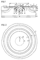
- the thyristor shown in FIGS. 1 and 2 has a weakly n-doped inner zone 1. This is followed by a p-doped base zone 2 on the cathode side.
- the base zone 2 has a recess 4.
- a layer 3 which has the same conduction type as the base zone 2. It extends to the surface on the cathode side.
- the layer 3 is preferably doped higher than the zone 2.
- an additional zone 5 which has the same conductivity type as the base zone 2 on the cathode side. It is connected to the layer 3 and is spaced on all sides from the edge of the recess 4, i. H. from base zone 2.
- An emitter zone 6 is embedded in the base zone 2, which can be the auxiliary emitter zone of an auxiliary thyristor, for example. It is contacted by an auxiliary emitter electrode 7. In addition, the auxiliary emitter electrode 7 also contacts the base zone 2 on the outside.
- the recess 4, the layer 3, the additional zone 5, the auxiliary emitter zone 6 and the electrode 7 can, as shown in FIG. 2, be circular or ring-shaped and arranged concentrically to one another.
- the pn junction 10 between additional zone 5 and inner zone 1 then has one in the plane of the surface of the thyristor Radius r2 ( Figure 2).
- the additional zone 5 can have the shape of a spherical cap with the radius r1 in the plane perpendicular to the surface of the thyristor (FIG. 1).
- zone 5 is not mandatory. You can also have the shape of a conventional diffusion trough and z. B. the shape of a polygon. It is essential, however, that the additional zone 5 is at least partially convex when viewed from the inner zone 1.
- zone 5 is simultaneously with the cathode-side base zone 2 z. B. manufactured by implanting a thin layer and subsequent driving.
- Layer 3 is e.g. B. also generated by implantation and driving.
- the shape of the recess 4, the zone 6 and the electrode 7 can also deviate from the circular shape or annular shape and z. B. be polygonal.
- Zone 3 is z. B. with a dose greater than 1012 / cm2 and then driving to z. B. a thickness of 5 microns.
- the depth d pn of the pn junctions 10, 11 of the additional zone 5 and the base zone 2 are greater than 40 ⁇ m.
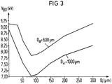
- FIG. 3 shows the relationship between the breakdown voltage V BO and the diameter D i of the additional zone 5. It can be seen that the breakdown voltage has a minimum for different diameters D a of the recess 4 at a diameter D i of approximately 80 ⁇ m. A reduction generally results when the diameter D i is smaller than half the diameter D a .
- the lower limit of D i is approximately 1/10 to 1/20 of the diameter D a , since the breakdown voltage increases again with a further decrease in the diameter D i . It has also proven to be expedient if the diameter D i of the additional zone is greater than half the depth (d pn ) of the pn junction of the additional zone.
- FIG. 1 it is shown that when a voltage is applied in the forward direction, charge pairs are preferably formed in the region of the additional zone 5, of which the electrons move to the anode-side emitter zone 8 and the holes to layer 3 and then under the auxiliary emitter zone 6 to the auxiliary emitter electrode 7.
- This current increases like an avalanche and initiates the ignition of the auxiliary thyristor and thus of the entire thyristor in a known manner.
- Layer 3 has the purpose of protecting the cathode-side surface of the thyristor from surface charges. For this purpose, as already mentioned, it is doped higher than the additional zone 5 and the base zone 2.
- the thyristor can be light-controllable. Its light-sensitive area 9 comprises the layer 3 and the zone 5, possibly also an area of the base zone 2 adjoining the layer 3. However, the invention can also be applied to current-controlled thyristors. Layer 3 or the base zone of one of the auxiliary thyristors mentioned at the beginning is then contacted by a gate electrode 12.
Landscapes
- Thyristors (AREA)
Abstract
Description
- In Hochspannungsanlagen sind im allgemeinen mehrere Thyristoren in Reihe geschaltet. Diese müssen stets gleichzeitig gezündet werden. Zündet einer der Thyristoren später, so liegt an ihm nahezu die gesamte Spannung an und der Thyristor wird zerstört. Man ist daher bemüht, Thyristoren zu entwickeln, die "über Kopf" gezündet werden können. Solche Thyristoren haben in aller Regel einen zentralen Bereich, der eine gegenüber dem übrigen Bereich und dem Rand niedrigere Durchbruchsspannung hat. Steigt die Spannung am Thyristor an, so geht dieser Bereich in den Avalanche-Durchbruch und der Durchbruchsstrom kann den Thyristor direkt oder über einen oder mehrere Hilfsthyristorstrukturen zünden.
- Der Durchbruchsbereich kann z. B. dadurch erzeugt werden, daß die katodenseitige Basiszone eine Aussparung hat, innerhalb der an der Oberfläche des Halbleiterkörpers eine dünnere Schicht des gleichen Leitfähigkeitstyp angeordnet ist. Der pn-Übergang zwischen der katodenseitigen Basiszone und der Innenzone hat dann beim Übergang von der Waagrechten in die Aussparung einen definierten Krümmungsradius, an dem eine gegenüber einem ebenen pn-Übergang höhere Feldstärke auftritt. An der Krümmung kommt es daher vorzugsweise zu einem Durchbruch des Thyristors. Eine Struktur dieser Art ist z. B. in dem Artikel "Design Consideration for High-Power, Overvoltage Self-Protected Thyristor" von Ohashi, Yoshida, Yamaguchi, Akagi, veröffentlicht in IPEC-Tokyo '83, Seiten 550 bis 558, insbesondere anhand von Figur 1B beschrieben worden.
- Die Durchbruchseigenschaften des genannten Bereichs hängen von der Form des pn-Übergangs der katodenseitigen Basiszone ab. Außerdem überlagert sich die Feldstärkeerhöhung durch den beschriebenen definierten Krümmungsradius mit einer Feldstärkeverminderung, die durch die zylindrische Form der Aussparung und die dünne Oberflächenschicht bedingt ist. Der beschriebene Bereich verminderter Durchbruchsspannung ist daher nur bei großer Eindringtiefe der katodenseitigen Basiszone wirksam. Wird die dünne Oberflächenschicht weggelassen, erhöht sich zwar die Wirksamkeit des Bereiches. Die Durchbruchsspannung hängt dann aber stark von Oberlächenladungen und damit von der Prozeßführung ab, so daß sie nicht gut reproduzierbar ist.
- Die Erfindung bezieht sich auf einen Thyristor mit einem Halbleiterkörper mit einer Innenzone vom ersten Leitungstyp und einer katodenseitigen Basiszone vom entgegengesetzten, zweiten Leitungstyp, mit einer Aussparung in der Basiszone, innerhalb der an der Oberfläche des Halbleiterkörpers eine gegenüber der Basiszone dünnere Schicht des zweiten Leitungstyps angeordnet ist, die mit der katodenseitigen Basiszone verbunden ist.
- Ziel der vorliegenden Erfindung ist es, einen Thyristor der geschilderten Art derart weiterzubilden, daß der Bereich verminderter Durchbruchsspannung besser reproduzierbar und wirksamer ist.
- Dieses Ziel wird dadurch erreicht, daß in der Aussparung eine zusätzliche Zone des zweiten Leitungstyps angeordnet ist, daß die Schicht mit der zusätzlichen Zone verbunden ist, daß die zusätzliche Zone dicker als die Schicht und im Abstand zur katodenseitigen Basiszone angeordnet ist.
- Weiterbildungen der Erfindung sind Gegenstand der Unteransprüche. Die Erfindung wird anhand eines Ausführungsbeispiels in Verbindung mit den Figuren 1 bis 3 näher erläutert. Es zeigen:
- Figur 1 und 2
- einen Schnitt durch und eine Aufsicht auf einen Thyristor gemäß der Erfindung und
- Figur 3
- ein Diagramm, das den Zusammenhang zwischen Durchbruchsspannung VBO und Durchmesser Di der zusätzlichen Zone mit dem Durchmesser Da der Aussparung als Parameter darstellt.
- Der in Figur 1 und 2 dargestellte Thyristor hat eine schwach n-dotierte Innenzone 1. An diese schließt sich eine p-dotierte katodenseitige Basiszone 2 an. Die Basiszone 2 hat eine Aussparung 4. In der Aussparung 4 sitzt eine Schicht 3, die den gleichen Leitungstyp wie die Basiszone 2 hat. Sie reicht bis an die katodenseitige Oberfläche. Vorzugsweise ist die Schicht 3 höher dotiert als die Zone 2. In der Aussparung 4 ist außerdem eine zusätzliche Zone 5 angeordnet, die den gleichen Leitungstyp wie die katodenseitige Basiszone 2 hat. Sie ist mit der Schicht 3 verbunden und hat allseitig einen Abstand vom Rand der Aussparung 4, d. h. von der Basiszone 2.
- In der Basiszone 2 ist eine Emitterzone 6 eingebettet, die beispielsweise die Hilfsemitterzone eines Hilfsthyristors sein kann. Sie ist durch eine Hilfsemitterelektrode 7 kontaktiert. Außerdem kontaktiert die Hilfsemitterelektrode 7 an der Außenseite auch die Basiszone 2.
- Die Aussparung 4, die Schicht 3, die zusätzliche Zone 5, die Hilfsemitterzone 6 und die Elektrode 7 können, wie in Figur 2 dargestellt, kreisförmig bzw. ringförmig ausgebildet und konzentrisch zueinander angeordnet sein. Der pn-Übergang 10 zwischen zusätzlicher Zone 5 und Innenzone 1 hat dann in der Ebene der Oberfläche des Thyristors einen Radius r2 (Figur 2). Die zusätzliche Zone 5 kann in der Ebene senkrecht zur Oberfläche des Thyristors (Figur 1) die Form einer Kugelkalotte mit dem Radius r1 haben.
- Die dargestellte Form der zusätzlichen Zone 5 ist jedoch nicht zwingend. Sie kann auch die Form einer üblichen Diffusionswanne haben und in der Aufsicht z. B. die Form eines Polygons. Wesentlich ist jedoch, daß die zusätzliche Zone 5 von der Innenzone 1 gesehen mindestens teilweise konvex ist. Zweckmäßigerweise wird die Zone 5 gleichzeitig mit der katodenseitigen Basiszone 2 z. B. durch Implantieren einer dünnen Schicht und nachfolgendes Eintreiben hergestellt. Die Schicht 3 wird z. B. ebenfalls durch Implantieren und Eintreiben erzeugt.
- Die Form der Aussparung 4, der Zone 6 und der Elektrode 7 können auch von der Kreisform bzw. Kreisringform abweichen und z. B. polygonal geformt sein.
- Für einen Thyristor von etwa 8 kV wurde eine Grunddotierung der Innenzone 1 von etwa 1 x 10¹³/cm³ eingestellt. Die katodenseitige Basiszone 2 kann eine Randdotierung größer 10¹⁶/cm³ haben. Die Zone 3 wird z. B. mit einer Dosis größer 10¹²/cm² und anschließendes Eintreiben auf z. B. eine Dicke von 5 µm hergestellt. Die Tiefe dpn der pn-Übergänge 10, 11 der zusätzlichen Zone 5 bzw. der Basiszone 2 sind größer 40 µm.
- In Figur 3 ist der Zusammenhang zwischen Durchbruchsspannung VBO und dem Durchmesser Di der zusätzlichen Zone 5 dargestellt. Es ist ersichtlich, daß für verschiedene Durchmesser Da der Aussparung 4 die Durchbruchsspannung bei etwa einem Durchmesser Di von etwa 80 µm ein Minimum hat. Eine Absenkung ergibt sich allgemein schon dann, wenn der Durchmesser Di kleiner als der halbe Durchmesser Da ist.
- Die untere Grenze von Di liegt bei etwa 1/10 bis 1/20 des Durchmessers Da, da bei weiterer Abnahme des Durchmessers Di die Durchbruchsspannung wieder ansteigt. Als zweckmäßig hat es sich außerdem erwiesen, wenn der Durchmesser Di der zusätzlichen Zone größer ist als die halbe Tiefe (dpn) des pn-Übergangs der zusätzlichen Zone.
- In Figur 1 ist dargestellt, daß sich bei Anlegen einer Spannung in Vorwärtsrichtung bevorzugt im Bereich der zusätzlichen Zone 5 Ladungsträgerpaare bilden, von denen sich die Elektronen zur anodenseitigen Emitterzone 8 und die Löcher zur Schicht 3 und dann unter der Hilfsemitterzone 6 zur Hilfsemitterelektrode 7 bewegen. Dieser Strom erhöht sich lawinenartig und leitet auf bekannte Weise die Zündung des Hilfsthyristors und damit des ganzen Thyristors ein.
- Die Schicht 3 hat den Zweck, die katodenseitige Oberfläche des Thyristors vor Oberflächenladungen zu schützen. Zu diesem Zweck ist sie, wie bereits erwähnt, höher dotiert als die zusätzliche Zone 5 und die Basiszone 2.
- Der Thyristor kann lichtsteuerbar sein. Sein lichtempfindlicher Bereich 9 umfaßt die Schicht 3 und die Zone 5, ggf. auch einen an die Schicht 3 angrenzenden Bereich der Basiszone 2. Die Erfindung läßt sich jedoch auch bei stromgesteuerten Thyristoren anwenden. Hier ist dann die Schicht 3 oder die Basiszone einer der eingangs erwähnten Hilfsthyristoren von einer Gateelektrode 12 kontaktiert.
Claims (9)
- Thyristor mit einem Halbleiterkörper mit einer Innenzone vom ersten Leitungstyp und einer katodenseitigen Basiszone vom entgegengesetzten, zweiten Leitungstyp, mit einer Aussparung in der Basiszone, innerhalb der an der Oberfläche des Halbleiterkörpers eine gegenüber der Basiszone dünnere Schicht des zweiten Leitungstyps angeordnet ist, die mit der katodenseitigen Basiszone verbunden ist,
dadurch gekennzeichnet, daß in der Aussparung (4) eine zusätzliche Zone (5) des zweiten Leitungstyps angeordnet ist, daß die Schicht (3) mit der zusatzlichen Zone (5) verbunden ist, daß die zusätzliche Zone (5) dicker als die Schicht (3) und im Abstand zur katodenseitigen Basiszone (2) angeordnet ist. - Thyristor nach Anspruch 1,
dadurch gekennzeichnet, daß die zusätzliche Zone und die Aussparung (4) in der Ebene der Oberfläche kreisförmig ausgebildet sind und daß die zusätzliche Zone konzentrisch in der Aussparung sitzt. - Thyristor nach Anspruch 2,
dadurch gekennzeichnet, daß der Durchmesser (Di) der zusätzlichen Zone kleiner als der halbe Durchmesser (Da) der Aussparung ist. - Thyristor nach einem der Ansprüche 1 bis 3,
dadurch gekennzeichnet, daß die zusätzliche Zone (5) die gleiche Tiefe (dpn) wie die katodenseitige Basiszone (2) hat. - Thyristor nach einem der Ansprüche 1 bis 4,
dadurch gekennzeichnet, daß die zusätzliche Zone (5) einen Durchmesser (Di) hat, der größer als die halbe Tiefe (dpn) des pn-Übergangs (10) der zusätzlichen Zone (5) hat. - Thyristor nach einem der Ansprüche 1 bis 5,
dadurch gekennzeichnet, daß er durch Licht steuerbar ist und daß die zusätzliche Zone (5) und die Schicht (3) im lichtempfindlichen Bereich (9) des Thyristors liegen. - Thyristor nach Anspruch 6,
dadurch gekennzeichnet, daß der lichtempfindliche Bereich (9) von einer Hilfsemitterzone (6) umgeben ist. - Thyristor nach einem der Ansprüche 1 bis 5,
dadurch gekennzeichnet, daß die Schicht (3) von einer Gateelektrode kontaktiert ist. - Thyristor nach einem der Ansprüche 1 bis 9,
dadurch gekennzeichnet, daß die Schicht (3) eine höhere Dotierung als die zusätzliche Zone (5) und die Basiszone (2) hat.
Applications Claiming Priority (2)
| Application Number | Priority Date | Filing Date | Title |
|---|---|---|---|
| DE4215378A DE4215378C1 (de) | 1992-05-11 | 1992-05-11 | Thyristor mit Durchbruchbereich |
| DE4215378 | 1992-05-11 |
Publications (2)
| Publication Number | Publication Date |
|---|---|
| EP0572826A1 true EP0572826A1 (de) | 1993-12-08 |
| EP0572826B1 EP0572826B1 (de) | 1999-08-04 |
Family
ID=6458531
Family Applications (1)
| Application Number | Title | Priority Date | Filing Date |
|---|---|---|---|
| EP93107690A Expired - Lifetime EP0572826B1 (de) | 1992-05-11 | 1993-05-11 | Thyristor mit Durchbruchbereich |
Country Status (5)
| Country | Link |
|---|---|
| US (1) | US5455434A (de) |
| EP (1) | EP0572826B1 (de) |
| JP (1) | JP3256021B2 (de) |
| CA (1) | CA2095769A1 (de) |
| DE (2) | DE4215378C1 (de) |
Cited By (4)
| Publication number | Priority date | Publication date | Assignee | Title |
|---|---|---|---|---|
| WO1998015010A1 (de) * | 1996-09-30 | 1998-04-09 | Eupec Europäische Gesellschaft Für Leistungshalbleiter Mbh + Co. Kg | Thyristor mit durchbruchbereich |
| US6066864A (en) * | 1996-05-20 | 2000-05-23 | Siemens Aktiengesellschaft | Thyristor with integrated dU/dt protection |
| DE10150640A1 (de) * | 2001-10-12 | 2003-04-30 | Eupec Gmbh & Co Kg | Thyristor mit integriertem Überkopfzündschutz |
| DE10135984B4 (de) * | 2001-07-24 | 2005-04-21 | eupec Europäische Gesellschaft für Leistungshalbleiter mbH & Co. KG | Anordnung mit einem lichtzündbaren Halbleiterbauelement und einem Teil zur Lichtdurchführung |
Families Citing this family (13)
| Publication number | Priority date | Publication date | Assignee | Title |
|---|---|---|---|---|
| JP2614601B2 (ja) * | 1994-06-03 | 1997-05-28 | 若築建設株式会社 | 鉄螺旋杭引抜き用ケーシング装置及び引抜き施工法 |
| JP3338234B2 (ja) * | 1995-05-17 | 2002-10-28 | 三菱電機株式会社 | 光トリガサイリスタ及びその製造方法 |
| US5610079A (en) * | 1995-06-19 | 1997-03-11 | Reliance Electric Industrial Company | Self-biased moat for parasitic current suppression in integrated circuits |
| DE19650762A1 (de) * | 1996-09-30 | 1998-07-02 | Eupec Gmbh & Co Kg | Thyristor mit Durchbruchbereich |
| DE10135983B4 (de) * | 2001-07-24 | 2005-05-04 | eupec Europäische Gesellschaft für Leistungshalbleiter mbH & Co. KG | Lichtzündbarer Thyristor |
| DE10231199A1 (de) * | 2002-07-10 | 2004-02-05 | eupec Europäische Gesellschaft für Leistungshalbleiter mbH | Halbleiterbauelement |
| DE10344592B4 (de) * | 2003-09-25 | 2006-01-12 | eupec Europäische Gesellschaft für Leistungshalbleiter mbH | Verfahren zum Einstellen der Durchbruchspannung eines Thyristors mit einer Durchbruchsstruktur |
| US8530964B2 (en) | 2011-12-08 | 2013-09-10 | Infineon Technologies Ag | Semiconductor device including first and second semiconductor elements |
| US8901647B2 (en) | 2011-12-08 | 2014-12-02 | Infineon Technologies Ag | Semiconductor device including first and second semiconductor elements |
| DE102018102234B4 (de) | 2018-02-01 | 2021-05-06 | Infineon Technologies Bipolar Gmbh & Co. Kg | Kurzschluss-Halbleiterbauelement |
| CN110265510B (zh) * | 2019-07-10 | 2024-04-05 | 兰州大学 | 一种深结雪崩倍增光控晶闸管及其触发控制系统 |
| EP3772111B1 (de) | 2019-08-01 | 2023-07-05 | Infineon Technologies Bipolar GmbH & Co. KG | Kurzschluss-halbleiterbauelement und verfahren zu dessen betrieb |
| DE102019124695A1 (de) | 2019-08-01 | 2021-02-04 | Infineon Technologies Bipolar Gmbh & Co. Kg | Kurzschluss-Halbleiterbauelement und Verfahren zu dessen Betrieb |
Citations (4)
| Publication number | Priority date | Publication date | Assignee | Title |
|---|---|---|---|---|
| EP0088967A2 (de) * | 1982-03-11 | 1983-09-21 | Westinghouse Electric Corporation | Verfahren zur Laserbehandlung für Thyristoren zum Selbstschutz gegen Uberspannung |
| DE3225991A1 (de) * | 1982-07-12 | 1984-01-12 | Licentia Patent-Verwaltungs-Gmbh, 6000 Frankfurt | Verfahren zur reduzierung der spannungsabhaengigkeit des spezifischen flaechenwiderstandes von si-zonen, welche sperrspannung aufnehmende pn-uebergaenge bilden |
| EP0129702A1 (de) * | 1983-05-26 | 1985-01-02 | General Electric Company | Gegen Fehlzündung geschützter Thyristor mit einer feldbegrenzenden Schicht in der Lawinendurchbruchsspannungszone |
| EP0316881A2 (de) * | 1987-11-20 | 1989-05-24 | Siemens Aktiengesellschaft | Thyristor mit einstellbarer Kippspannung |
Family Cites Families (4)
| Publication number | Priority date | Publication date | Assignee | Title |
|---|---|---|---|---|
| JPS55111168A (en) * | 1979-02-21 | 1980-08-27 | Meidensha Electric Mfg Co Ltd | Turn-off thyristor |
| US4516315A (en) * | 1983-05-09 | 1985-05-14 | Westinghouse Electric Corp. | Method of making a self-protected thyristor |
| JPS63284856A (ja) * | 1987-05-18 | 1988-11-22 | Hitachi Ltd | 埋込みゲ−ト型gtoサイリスタ |
| DE59010429D1 (de) * | 1990-03-12 | 1996-08-29 | Siemens Ag | Thyristor mit reflexionsarmer Lichtzündstruktur |
-
1992
- 1992-05-11 DE DE4215378A patent/DE4215378C1/de not_active Expired - Fee Related
-
1993
- 1993-05-07 CA CA002095769A patent/CA2095769A1/en not_active Abandoned
- 1993-05-10 JP JP10816993A patent/JP3256021B2/ja not_active Expired - Fee Related
- 1993-05-11 DE DE59309712T patent/DE59309712D1/de not_active Expired - Lifetime
- 1993-05-11 EP EP93107690A patent/EP0572826B1/de not_active Expired - Lifetime
-
1994
- 1994-08-08 US US08/286,987 patent/US5455434A/en not_active Expired - Lifetime
Patent Citations (4)
| Publication number | Priority date | Publication date | Assignee | Title |
|---|---|---|---|---|
| EP0088967A2 (de) * | 1982-03-11 | 1983-09-21 | Westinghouse Electric Corporation | Verfahren zur Laserbehandlung für Thyristoren zum Selbstschutz gegen Uberspannung |
| DE3225991A1 (de) * | 1982-07-12 | 1984-01-12 | Licentia Patent-Verwaltungs-Gmbh, 6000 Frankfurt | Verfahren zur reduzierung der spannungsabhaengigkeit des spezifischen flaechenwiderstandes von si-zonen, welche sperrspannung aufnehmende pn-uebergaenge bilden |
| EP0129702A1 (de) * | 1983-05-26 | 1985-01-02 | General Electric Company | Gegen Fehlzündung geschützter Thyristor mit einer feldbegrenzenden Schicht in der Lawinendurchbruchsspannungszone |
| EP0316881A2 (de) * | 1987-11-20 | 1989-05-24 | Siemens Aktiengesellschaft | Thyristor mit einstellbarer Kippspannung |
Non-Patent Citations (2)
| Title |
|---|
| PATENT ABSTRACTS OF JAPAN vol. 6, no. 238 (E-144)(1116) 26. November 1982 & JP-A 57 138 175 ( HITACHI SEISAKUSHO K.K. ) 26. August 1982 * |
| RESEARCH DISCLOSURE Nr. 302, Juni 1989, HAVANT GB Seite 449 'Method for achieving an overvoltage-protected thyristor' * |
Cited By (6)
| Publication number | Priority date | Publication date | Assignee | Title |
|---|---|---|---|---|
| US6066864A (en) * | 1996-05-20 | 2000-05-23 | Siemens Aktiengesellschaft | Thyristor with integrated dU/dt protection |
| WO1998015010A1 (de) * | 1996-09-30 | 1998-04-09 | Eupec Europäische Gesellschaft Für Leistungshalbleiter Mbh + Co. Kg | Thyristor mit durchbruchbereich |
| US6373079B1 (en) | 1996-09-30 | 2002-04-16 | Eupec Europaeische Gesellschaft Fur Leistungshalbleiter Mbh+Co.Kg | Thyristor with breakdown region |
| DE10135984B4 (de) * | 2001-07-24 | 2005-04-21 | eupec Europäische Gesellschaft für Leistungshalbleiter mbH & Co. KG | Anordnung mit einem lichtzündbaren Halbleiterbauelement und einem Teil zur Lichtdurchführung |
| DE10150640A1 (de) * | 2001-10-12 | 2003-04-30 | Eupec Gmbh & Co Kg | Thyristor mit integriertem Überkopfzündschutz |
| DE10150640B4 (de) * | 2001-10-12 | 2005-02-10 | eupec Europäische Gesellschaft für Leistungshalbleiter mbH & Co. KG | Thyristor mit integriertem Überkopfzündschutz und Verfahren zu seiner Herstellung |
Also Published As
| Publication number | Publication date |
|---|---|
| DE4215378C1 (de) | 1993-09-30 |
| EP0572826B1 (de) | 1999-08-04 |
| JPH0629519A (ja) | 1994-02-04 |
| US5455434A (en) | 1995-10-03 |
| DE59309712D1 (de) | 1999-09-09 |
| JP3256021B2 (ja) | 2002-02-12 |
| CA2095769A1 (en) | 1993-11-12 |
Similar Documents
| Publication | Publication Date | Title |
|---|---|---|
| EP0572826B1 (de) | Thyristor mit Durchbruchbereich | |
| EP0200863B1 (de) | Halbleiterbauelement mit Thyristor- und Diodenstrukturen | |
| EP0343369A1 (de) | Verfahren zum Herstellen eines Thyristors | |
| EP1131852B1 (de) | Halbleiterbauelement mit dielektrischen oder halbisolierenden abschirmstrukturen | |
| DE69316960T2 (de) | Elektronenröhre mit Halbleiterkathode | |
| EP0931351B1 (de) | Thyristor mit durchbruchbereich | |
| DE2511281A1 (de) | Durch licht aktivierbarer, steuerbarer halbleitergleichrichter | |
| DE3240564A1 (de) | Steuerbares halbleiterschaltelement | |
| EP0564007A1 (de) | Thyristor mit reduzierter Kippspannung | |
| EP0332955A2 (de) | Thyristor mit hoher positiver und negativer Sperrfähigkeit und Verfahren zu dessen Herstellung | |
| DE3787848T2 (de) | Halbleiterdiode. | |
| EP0049445A2 (de) | Selbstzündender Thyristor | |
| EP0430133B1 (de) | Leistungs-Halbleiterbauelement mit Emitterkurzschlüssen | |
| EP1216488B1 (de) | Thyristor mit spannungsstossbelastbarkeit in der freiwerdezeit | |
| DE19650762A1 (de) | Thyristor mit Durchbruchbereich | |
| EP0206350B1 (de) | Thyristor mit verminderter Mittelzonendicke | |
| EP0902979B1 (de) | Thyristor mit integriertem du/dt-schutz | |
| EP0062099A2 (de) | Thyristor und Verfahren zu seinem Betrieb | |
| WO1992017907A1 (de) | Thyristor mit einstellbarer kippspannung und verfahren zu seiner herstellung | |
| DE2746406C2 (de) | Thyristor mit innerer Zündverstärkung und hohem dV/dt-Wert | |
| WO2000075963A2 (de) | Thyristor mit integriertem freiwerdezeitschutz und herstellungsverfahren dafür | |
| DE1210490B (de) | Steuerbares Halbleiterbauelement mit einer pnpn- oder npnp-Zonenfolge und Verfahren zum Herstellen | |
| DE3853852T2 (de) | Thyristoren. | |
| DE3405549A1 (de) | Ueberspannungsgeschuetzter thyristor und verfahren zu seiner herstellung | |
| EP0310836A2 (de) | Halbleiterbauelement mit einem planaren pn-Übergang |
Legal Events
| Date | Code | Title | Description |
|---|---|---|---|
| PUAI | Public reference made under article 153(3) epc to a published international application that has entered the european phase |
Free format text: ORIGINAL CODE: 0009012 |
|
| AK | Designated contracting states |
Kind code of ref document: A1 Designated state(s): CH DE FR GB IT LI SE |
|
| 17P | Request for examination filed |
Effective date: 19940519 |
|
| 17Q | First examination report despatched |
Effective date: 19950804 |
|
| GRAG | Despatch of communication of intention to grant |
Free format text: ORIGINAL CODE: EPIDOS AGRA |
|
| GRAG | Despatch of communication of intention to grant |
Free format text: ORIGINAL CODE: EPIDOS AGRA |
|
| GRAH | Despatch of communication of intention to grant a patent |
Free format text: ORIGINAL CODE: EPIDOS IGRA |
|
| GRAH | Despatch of communication of intention to grant a patent |
Free format text: ORIGINAL CODE: EPIDOS IGRA |
|
| GRAA | (expected) grant |
Free format text: ORIGINAL CODE: 0009210 |
|
| AK | Designated contracting states |
Kind code of ref document: B1 Designated state(s): CH DE FR GB IT LI SE |
|
| PG25 | Lapsed in a contracting state [announced via postgrant information from national office to epo] |
Ref country code: SE Free format text: THE PATENT HAS BEEN ANNULLED BY A DECISION OF A NATIONAL AUTHORITY Effective date: 19990804 Ref country code: IT Free format text: LAPSE BECAUSE OF FAILURE TO SUBMIT A TRANSLATION OF THE DESCRIPTION OR TO PAY THE FEE WITHIN THE PRE;WARNING: LAPSES OF ITALIAN PATENTS WITH EFFECTIVE DATE BEFORE 2007 MAY HAVE OCCURRED AT ANY TIME BEFORE 2007. THE CORRECT EFFECTIVE DATE MAY BE DIFFERENT FROM THE ONE RECORDED.SCRIBED TIME-LIMIT Effective date: 19990804 |
|
| REG | Reference to a national code |
Ref country code: CH Ref legal event code: EP |
|
| REF | Corresponds to: |
Ref document number: 59309712 Country of ref document: DE Date of ref document: 19990909 |
|
| ET | Fr: translation filed | ||
| PG25 | Lapsed in a contracting state [announced via postgrant information from national office to epo] |
Ref country code: LI Free format text: LAPSE BECAUSE OF NON-PAYMENT OF DUE FEES Effective date: 20000531 Ref country code: CH Free format text: LAPSE BECAUSE OF NON-PAYMENT OF DUE FEES Effective date: 20000531 |
|
| PLBE | No opposition filed within time limit |
Free format text: ORIGINAL CODE: 0009261 |
|
| 26N | No opposition filed | ||
| REG | Reference to a national code |
Ref country code: CH Ref legal event code: PL |
|
| REG | Reference to a national code |
Ref country code: GB Ref legal event code: IF02 |
|
| PGFP | Annual fee paid to national office [announced via postgrant information from national office to epo] |
Ref country code: FR Payment date: 20090513 Year of fee payment: 17 |
|
| REG | Reference to a national code |
Ref country code: FR Ref legal event code: ST Effective date: 20110131 |
|
| PG25 | Lapsed in a contracting state [announced via postgrant information from national office to epo] |
Ref country code: FR Free format text: LAPSE BECAUSE OF NON-PAYMENT OF DUE FEES Effective date: 20100531 |
|
| REG | Reference to a national code |
Ref country code: GB Ref legal event code: 732E Free format text: REGISTERED BETWEEN 20110707 AND 20110713 |
|
| REG | Reference to a national code |
Ref country code: FR Ref legal event code: TP Owner name: INFINEON TECHNOLOGIES AG, DE Effective date: 20110922 |
|
| REG | Reference to a national code |
Ref country code: DE Ref legal event code: R081 Ref document number: 59309712 Country of ref document: DE Owner name: INFINEON TECHNOLOGIES AG, DE Free format text: FORMER OWNER: SIEMENS AKTIENGESELLSCHAFT, 80333 MUENCHEN, DE Effective date: 20111107 |
|
| PGFP | Annual fee paid to national office [announced via postgrant information from national office to epo] |
Ref country code: GB Payment date: 20120522 Year of fee payment: 20 |
|
| PGFP | Annual fee paid to national office [announced via postgrant information from national office to epo] |
Ref country code: DE Payment date: 20120725 Year of fee payment: 20 |
|
| REG | Reference to a national code |
Ref country code: DE Ref legal event code: R071 Ref document number: 59309712 Country of ref document: DE |
|
| REG | Reference to a national code |
Ref country code: GB Ref legal event code: PE20 Expiry date: 20130510 |
|
| PG25 | Lapsed in a contracting state [announced via postgrant information from national office to epo] |
Ref country code: DE Free format text: LAPSE BECAUSE OF EXPIRATION OF PROTECTION Effective date: 20130514 Ref country code: GB Free format text: LAPSE BECAUSE OF EXPIRATION OF PROTECTION Effective date: 20130510 |