EP0571978B1 - Heater element for a tube connecting device - Google Patents
Heater element for a tube connecting device Download PDFInfo
- Publication number
- EP0571978B1 EP0571978B1 EP19930108501 EP93108501A EP0571978B1 EP 0571978 B1 EP0571978 B1 EP 0571978B1 EP 19930108501 EP19930108501 EP 19930108501 EP 93108501 A EP93108501 A EP 93108501A EP 0571978 B1 EP0571978 B1 EP 0571978B1
- Authority
- EP
- European Patent Office
- Prior art keywords
- resistor
- heater element
- element according
- conductive paste
- insulation layer
- Prior art date
- Legal status (The legal status is an assumption and is not a legal conclusion. Google has not performed a legal analysis and makes no representation as to the accuracy of the status listed.)
- Expired - Lifetime
Links
Images


Classifications
-
- A—HUMAN NECESSITIES
- A61—MEDICAL OR VETERINARY SCIENCE; HYGIENE
- A61M—DEVICES FOR INTRODUCING MEDIA INTO, OR ONTO, THE BODY; DEVICES FOR TRANSDUCING BODY MEDIA OR FOR TAKING MEDIA FROM THE BODY; DEVICES FOR PRODUCING OR ENDING SLEEP OR STUPOR
- A61M39/00—Tubes, tube connectors, tube couplings, valves, access sites or the like, specially adapted for medical use
- A61M39/10—Tube connectors; Tube couplings
- A61M39/14—Tube connectors; Tube couplings for connecting tubes having sealed ends
- A61M39/146—Tube connectors; Tube couplings for connecting tubes having sealed ends by cutting and welding
-
- B—PERFORMING OPERATIONS; TRANSPORTING
- B29—WORKING OF PLASTICS; WORKING OF SUBSTANCES IN A PLASTIC STATE IN GENERAL
- B29C—SHAPING OR JOINING OF PLASTICS; SHAPING OF MATERIAL IN A PLASTIC STATE, NOT OTHERWISE PROVIDED FOR; AFTER-TREATMENT OF THE SHAPED PRODUCTS, e.g. REPAIRING
- B29C65/00—Joining or sealing of preformed parts, e.g. welding of plastics materials; Apparatus therefor
- B29C65/02—Joining or sealing of preformed parts, e.g. welding of plastics materials; Apparatus therefor by heating, with or without pressure
- B29C65/18—Joining or sealing of preformed parts, e.g. welding of plastics materials; Apparatus therefor by heating, with or without pressure using heated tools
- B29C65/20—Joining or sealing of preformed parts, e.g. welding of plastics materials; Apparatus therefor by heating, with or without pressure using heated tools with direct contact, e.g. using "mirror"
- B29C65/2046—Joining or sealing of preformed parts, e.g. welding of plastics materials; Apparatus therefor by heating, with or without pressure using heated tools with direct contact, e.g. using "mirror" using a welding mirror which also cuts the parts to be joined, e.g. for sterile welding
-
- B—PERFORMING OPERATIONS; TRANSPORTING
- B29—WORKING OF PLASTICS; WORKING OF SUBSTANCES IN A PLASTIC STATE IN GENERAL
- B29C—SHAPING OR JOINING OF PLASTICS; SHAPING OF MATERIAL IN A PLASTIC STATE, NOT OTHERWISE PROVIDED FOR; AFTER-TREATMENT OF THE SHAPED PRODUCTS, e.g. REPAIRING
- B29C65/00—Joining or sealing of preformed parts, e.g. welding of plastics materials; Apparatus therefor
- B29C65/02—Joining or sealing of preformed parts, e.g. welding of plastics materials; Apparatus therefor by heating, with or without pressure
- B29C65/18—Joining or sealing of preformed parts, e.g. welding of plastics materials; Apparatus therefor by heating, with or without pressure using heated tools
- B29C65/20—Joining or sealing of preformed parts, e.g. welding of plastics materials; Apparatus therefor by heating, with or without pressure using heated tools with direct contact, e.g. using "mirror"
- B29C65/2053—Joining or sealing of preformed parts, e.g. welding of plastics materials; Apparatus therefor by heating, with or without pressure using heated tools with direct contact, e.g. using "mirror" characterised by special ways of bringing the welding mirrors into position
- B29C65/2061—Joining or sealing of preformed parts, e.g. welding of plastics materials; Apparatus therefor by heating, with or without pressure using heated tools with direct contact, e.g. using "mirror" characterised by special ways of bringing the welding mirrors into position by sliding
- B29C65/2069—Joining or sealing of preformed parts, e.g. welding of plastics materials; Apparatus therefor by heating, with or without pressure using heated tools with direct contact, e.g. using "mirror" characterised by special ways of bringing the welding mirrors into position by sliding with an angle with respect to the plane comprising the parts to be joined
- B29C65/2076—Joining or sealing of preformed parts, e.g. welding of plastics materials; Apparatus therefor by heating, with or without pressure using heated tools with direct contact, e.g. using "mirror" characterised by special ways of bringing the welding mirrors into position by sliding with an angle with respect to the plane comprising the parts to be joined perpendicularly to the plane comprising the parts to be joined
-
- B—PERFORMING OPERATIONS; TRANSPORTING
- B29—WORKING OF PLASTICS; WORKING OF SUBSTANCES IN A PLASTIC STATE IN GENERAL
- B29C—SHAPING OR JOINING OF PLASTICS; SHAPING OF MATERIAL IN A PLASTIC STATE, NOT OTHERWISE PROVIDED FOR; AFTER-TREATMENT OF THE SHAPED PRODUCTS, e.g. REPAIRING
- B29C65/00—Joining or sealing of preformed parts, e.g. welding of plastics materials; Apparatus therefor
- B29C65/02—Joining or sealing of preformed parts, e.g. welding of plastics materials; Apparatus therefor by heating, with or without pressure
- B29C65/18—Joining or sealing of preformed parts, e.g. welding of plastics materials; Apparatus therefor by heating, with or without pressure using heated tools
- B29C65/22—Heated wire resistive ribbon, resistive band or resistive strip
- B29C65/221—Heated wire resistive ribbon, resistive band or resistive strip characterised by the type of heated wire, resistive ribbon, band or strip
- B29C65/225—Heated wire resistive ribbon, resistive band or resistive strip characterised by the type of heated wire, resistive ribbon, band or strip being a coating or being printed, e.g. being applied as a paint or forming a printed circuit
-
- B—PERFORMING OPERATIONS; TRANSPORTING
- B29—WORKING OF PLASTICS; WORKING OF SUBSTANCES IN A PLASTIC STATE IN GENERAL
- B29C—SHAPING OR JOINING OF PLASTICS; SHAPING OF MATERIAL IN A PLASTIC STATE, NOT OTHERWISE PROVIDED FOR; AFTER-TREATMENT OF THE SHAPED PRODUCTS, e.g. REPAIRING
- B29C65/00—Joining or sealing of preformed parts, e.g. welding of plastics materials; Apparatus therefor
- B29C65/02—Joining or sealing of preformed parts, e.g. welding of plastics materials; Apparatus therefor by heating, with or without pressure
- B29C65/18—Joining or sealing of preformed parts, e.g. welding of plastics materials; Apparatus therefor by heating, with or without pressure using heated tools
- B29C65/22—Heated wire resistive ribbon, resistive band or resistive strip
- B29C65/228—Heated wire resistive ribbon, resistive band or resistive strip characterised by the means for electrically connecting the ends of said heated wire, resistive ribbon, resistive band or resistive strip
-
- B—PERFORMING OPERATIONS; TRANSPORTING
- B29—WORKING OF PLASTICS; WORKING OF SUBSTANCES IN A PLASTIC STATE IN GENERAL
- B29C—SHAPING OR JOINING OF PLASTICS; SHAPING OF MATERIAL IN A PLASTIC STATE, NOT OTHERWISE PROVIDED FOR; AFTER-TREATMENT OF THE SHAPED PRODUCTS, e.g. REPAIRING
- B29C65/00—Joining or sealing of preformed parts, e.g. welding of plastics materials; Apparatus therefor
- B29C65/02—Joining or sealing of preformed parts, e.g. welding of plastics materials; Apparatus therefor by heating, with or without pressure
- B29C65/18—Joining or sealing of preformed parts, e.g. welding of plastics materials; Apparatus therefor by heating, with or without pressure using heated tools
- B29C65/24—Joining or sealing of preformed parts, e.g. welding of plastics materials; Apparatus therefor by heating, with or without pressure using heated tools characterised by the means for heating the tool
- B29C65/30—Electrical means
-
- B—PERFORMING OPERATIONS; TRANSPORTING
- B29—WORKING OF PLASTICS; WORKING OF SUBSTANCES IN A PLASTIC STATE IN GENERAL
- B29C—SHAPING OR JOINING OF PLASTICS; SHAPING OF MATERIAL IN A PLASTIC STATE, NOT OTHERWISE PROVIDED FOR; AFTER-TREATMENT OF THE SHAPED PRODUCTS, e.g. REPAIRING
- B29C65/00—Joining or sealing of preformed parts, e.g. welding of plastics materials; Apparatus therefor
- B29C65/78—Means for handling the parts to be joined, e.g. for making containers or hollow articles, e.g. means for handling sheets, plates, web-like materials, tubular articles, hollow articles or elements to be joined therewith; Means for discharging the joined articles from the joining apparatus
- B29C65/7802—Positioning the parts to be joined, e.g. aligning, indexing or centring
-
- B—PERFORMING OPERATIONS; TRANSPORTING
- B29—WORKING OF PLASTICS; WORKING OF SUBSTANCES IN A PLASTIC STATE IN GENERAL
- B29C—SHAPING OR JOINING OF PLASTICS; SHAPING OF MATERIAL IN A PLASTIC STATE, NOT OTHERWISE PROVIDED FOR; AFTER-TREATMENT OF THE SHAPED PRODUCTS, e.g. REPAIRING
- B29C65/00—Joining or sealing of preformed parts, e.g. welding of plastics materials; Apparatus therefor
- B29C65/78—Means for handling the parts to be joined, e.g. for making containers or hollow articles, e.g. means for handling sheets, plates, web-like materials, tubular articles, hollow articles or elements to be joined therewith; Means for discharging the joined articles from the joining apparatus
- B29C65/7841—Holding or clamping means for handling purposes
-
- B—PERFORMING OPERATIONS; TRANSPORTING
- B29—WORKING OF PLASTICS; WORKING OF SUBSTANCES IN A PLASTIC STATE IN GENERAL
- B29C—SHAPING OR JOINING OF PLASTICS; SHAPING OF MATERIAL IN A PLASTIC STATE, NOT OTHERWISE PROVIDED FOR; AFTER-TREATMENT OF THE SHAPED PRODUCTS, e.g. REPAIRING
- B29C66/00—General aspects of processes or apparatus for joining preformed parts
- B29C66/001—Joining in special atmospheres
- B29C66/0012—Joining in special atmospheres characterised by the type of environment
- B29C66/0018—Joining in special atmospheres characterised by the type of environment being sterile
-
- B—PERFORMING OPERATIONS; TRANSPORTING
- B29—WORKING OF PLASTICS; WORKING OF SUBSTANCES IN A PLASTIC STATE IN GENERAL
- B29C—SHAPING OR JOINING OF PLASTICS; SHAPING OF MATERIAL IN A PLASTIC STATE, NOT OTHERWISE PROVIDED FOR; AFTER-TREATMENT OF THE SHAPED PRODUCTS, e.g. REPAIRING
- B29C66/00—General aspects of processes or apparatus for joining preformed parts
- B29C66/01—General aspects dealing with the joint area or with the area to be joined
- B29C66/05—Particular design of joint configurations
- B29C66/10—Particular design of joint configurations particular design of the joint cross-sections
- B29C66/11—Joint cross-sections comprising a single joint-segment, i.e. one of the parts to be joined comprising a single joint-segment in the joint cross-section
- B29C66/114—Single butt joints
- B29C66/1142—Single butt to butt joints
-
- B—PERFORMING OPERATIONS; TRANSPORTING
- B29—WORKING OF PLASTICS; WORKING OF SUBSTANCES IN A PLASTIC STATE IN GENERAL
- B29C—SHAPING OR JOINING OF PLASTICS; SHAPING OF MATERIAL IN A PLASTIC STATE, NOT OTHERWISE PROVIDED FOR; AFTER-TREATMENT OF THE SHAPED PRODUCTS, e.g. REPAIRING
- B29C66/00—General aspects of processes or apparatus for joining preformed parts
- B29C66/50—General aspects of joining tubular articles; General aspects of joining long products, i.e. bars or profiled elements; General aspects of joining single elements to tubular articles, hollow articles or bars; General aspects of joining several hollow-preforms to form hollow or tubular articles
- B29C66/51—Joining tubular articles, profiled elements or bars; Joining single elements to tubular articles, hollow articles or bars; Joining several hollow-preforms to form hollow or tubular articles
- B29C66/52—Joining tubular articles, bars or profiled elements
- B29C66/522—Joining tubular articles
- B29C66/5221—Joining tubular articles for forming coaxial connections, i.e. the tubular articles to be joined forming a zero angle relative to each other
-
- B—PERFORMING OPERATIONS; TRANSPORTING
- B29—WORKING OF PLASTICS; WORKING OF SUBSTANCES IN A PLASTIC STATE IN GENERAL
- B29C—SHAPING OR JOINING OF PLASTICS; SHAPING OF MATERIAL IN A PLASTIC STATE, NOT OTHERWISE PROVIDED FOR; AFTER-TREATMENT OF THE SHAPED PRODUCTS, e.g. REPAIRING
- B29C66/00—General aspects of processes or apparatus for joining preformed parts
- B29C66/70—General aspects of processes or apparatus for joining preformed parts characterised by the composition, physical properties or the structure of the material of the parts to be joined; Joining with non-plastics material
- B29C66/73—General aspects of processes or apparatus for joining preformed parts characterised by the composition, physical properties or the structure of the material of the parts to be joined; Joining with non-plastics material characterised by the intensive physical properties of the material of the parts to be joined, by the optical properties of the material of the parts to be joined, by the extensive physical properties of the parts to be joined, by the state of the material of the parts to be joined or by the material of the parts to be joined being a thermoplastic or a thermoset
- B29C66/737—General aspects of processes or apparatus for joining preformed parts characterised by the composition, physical properties or the structure of the material of the parts to be joined; Joining with non-plastics material characterised by the intensive physical properties of the material of the parts to be joined, by the optical properties of the material of the parts to be joined, by the extensive physical properties of the parts to be joined, by the state of the material of the parts to be joined or by the material of the parts to be joined being a thermoplastic or a thermoset characterised by the state of the material of the parts to be joined
- B29C66/7373—Joining soiled or oxidised materials
-
- B—PERFORMING OPERATIONS; TRANSPORTING
- B29—WORKING OF PLASTICS; WORKING OF SUBSTANCES IN A PLASTIC STATE IN GENERAL
- B29C—SHAPING OR JOINING OF PLASTICS; SHAPING OF MATERIAL IN A PLASTIC STATE, NOT OTHERWISE PROVIDED FOR; AFTER-TREATMENT OF THE SHAPED PRODUCTS, e.g. REPAIRING
- B29C66/00—General aspects of processes or apparatus for joining preformed parts
- B29C66/70—General aspects of processes or apparatus for joining preformed parts characterised by the composition, physical properties or the structure of the material of the parts to be joined; Joining with non-plastics material
- B29C66/73—General aspects of processes or apparatus for joining preformed parts characterised by the composition, physical properties or the structure of the material of the parts to be joined; Joining with non-plastics material characterised by the intensive physical properties of the material of the parts to be joined, by the optical properties of the material of the parts to be joined, by the extensive physical properties of the parts to be joined, by the state of the material of the parts to be joined or by the material of the parts to be joined being a thermoplastic or a thermoset
- B29C66/739—General aspects of processes or apparatus for joining preformed parts characterised by the composition, physical properties or the structure of the material of the parts to be joined; Joining with non-plastics material characterised by the intensive physical properties of the material of the parts to be joined, by the optical properties of the material of the parts to be joined, by the extensive physical properties of the parts to be joined, by the state of the material of the parts to be joined or by the material of the parts to be joined being a thermoplastic or a thermoset characterised by the material of the parts to be joined being a thermoplastic or a thermoset
- B29C66/7392—General aspects of processes or apparatus for joining preformed parts characterised by the composition, physical properties or the structure of the material of the parts to be joined; Joining with non-plastics material characterised by the intensive physical properties of the material of the parts to be joined, by the optical properties of the material of the parts to be joined, by the extensive physical properties of the parts to be joined, by the state of the material of the parts to be joined or by the material of the parts to be joined being a thermoplastic or a thermoset characterised by the material of the parts to be joined being a thermoplastic or a thermoset characterised by the material of at least one of the parts being a thermoplastic
- B29C66/73921—General aspects of processes or apparatus for joining preformed parts characterised by the composition, physical properties or the structure of the material of the parts to be joined; Joining with non-plastics material characterised by the intensive physical properties of the material of the parts to be joined, by the optical properties of the material of the parts to be joined, by the extensive physical properties of the parts to be joined, by the state of the material of the parts to be joined or by the material of the parts to be joined being a thermoplastic or a thermoset characterised by the material of the parts to be joined being a thermoplastic or a thermoset characterised by the material of at least one of the parts being a thermoplastic characterised by the materials of both parts being thermoplastics
-
- B—PERFORMING OPERATIONS; TRANSPORTING
- B29—WORKING OF PLASTICS; WORKING OF SUBSTANCES IN A PLASTIC STATE IN GENERAL
- B29C—SHAPING OR JOINING OF PLASTICS; SHAPING OF MATERIAL IN A PLASTIC STATE, NOT OTHERWISE PROVIDED FOR; AFTER-TREATMENT OF THE SHAPED PRODUCTS, e.g. REPAIRING
- B29C66/00—General aspects of processes or apparatus for joining preformed parts
- B29C66/80—General aspects of machine operations or constructions and parts thereof
- B29C66/81—General aspects of the pressing elements, i.e. the elements applying pressure on the parts to be joined in the area to be joined, e.g. the welding jaws or clamps
- B29C66/816—General aspects of the pressing elements, i.e. the elements applying pressure on the parts to be joined in the area to be joined, e.g. the welding jaws or clamps characterised by the mounting of the pressing elements, e.g. of the welding jaws or clamps
- B29C66/8167—Quick change joining tools or surfaces
-
- B—PERFORMING OPERATIONS; TRANSPORTING
- B29—WORKING OF PLASTICS; WORKING OF SUBSTANCES IN A PLASTIC STATE IN GENERAL
- B29C—SHAPING OR JOINING OF PLASTICS; SHAPING OF MATERIAL IN A PLASTIC STATE, NOT OTHERWISE PROVIDED FOR; AFTER-TREATMENT OF THE SHAPED PRODUCTS, e.g. REPAIRING
- B29C66/00—General aspects of processes or apparatus for joining preformed parts
- B29C66/80—General aspects of machine operations or constructions and parts thereof
- B29C66/81—General aspects of the pressing elements, i.e. the elements applying pressure on the parts to be joined in the area to be joined, e.g. the welding jaws or clamps
- B29C66/818—General aspects of the pressing elements, i.e. the elements applying pressure on the parts to be joined in the area to be joined, e.g. the welding jaws or clamps characterised by the cooling constructional aspects, or by the thermal or electrical insulating or conducting constructional aspects of the welding jaws or of the clamps ; comprising means for compensating for the thermal expansion of the welding jaws or of the clamps
- B29C66/8187—General aspects of the pressing elements, i.e. the elements applying pressure on the parts to be joined in the area to be joined, e.g. the welding jaws or clamps characterised by the cooling constructional aspects, or by the thermal or electrical insulating or conducting constructional aspects of the welding jaws or of the clamps ; comprising means for compensating for the thermal expansion of the welding jaws or of the clamps characterised by the electrical insulating constructional aspects
- B29C66/81871—General aspects of the pressing elements, i.e. the elements applying pressure on the parts to be joined in the area to be joined, e.g. the welding jaws or clamps characterised by the cooling constructional aspects, or by the thermal or electrical insulating or conducting constructional aspects of the welding jaws or of the clamps ; comprising means for compensating for the thermal expansion of the welding jaws or of the clamps characterised by the electrical insulating constructional aspects of the welding jaws
-
- B—PERFORMING OPERATIONS; TRANSPORTING
- B29—WORKING OF PLASTICS; WORKING OF SUBSTANCES IN A PLASTIC STATE IN GENERAL
- B29C—SHAPING OR JOINING OF PLASTICS; SHAPING OF MATERIAL IN A PLASTIC STATE, NOT OTHERWISE PROVIDED FOR; AFTER-TREATMENT OF THE SHAPED PRODUCTS, e.g. REPAIRING
- B29C66/00—General aspects of processes or apparatus for joining preformed parts
- B29C66/80—General aspects of machine operations or constructions and parts thereof
- B29C66/84—Specific machine types or machines suitable for specific applications
- B29C66/857—Medical tube welding machines
-
- B—PERFORMING OPERATIONS; TRANSPORTING
- B29—WORKING OF PLASTICS; WORKING OF SUBSTANCES IN A PLASTIC STATE IN GENERAL
- B29C—SHAPING OR JOINING OF PLASTICS; SHAPING OF MATERIAL IN A PLASTIC STATE, NOT OTHERWISE PROVIDED FOR; AFTER-TREATMENT OF THE SHAPED PRODUCTS, e.g. REPAIRING
- B29C66/00—General aspects of processes or apparatus for joining preformed parts
- B29C66/90—Measuring or controlling the joining process
- B29C66/91—Measuring or controlling the joining process by measuring or controlling the temperature, the heat or the thermal flux
- B29C66/914—Measuring or controlling the joining process by measuring or controlling the temperature, the heat or the thermal flux by controlling or regulating the temperature, the heat or the thermal flux
- B29C66/9141—Measuring or controlling the joining process by measuring or controlling the temperature, the heat or the thermal flux by controlling or regulating the temperature, the heat or the thermal flux by controlling or regulating the temperature
- B29C66/91421—Measuring or controlling the joining process by measuring or controlling the temperature, the heat or the thermal flux by controlling or regulating the temperature, the heat or the thermal flux by controlling or regulating the temperature of the joining tools
-
- B—PERFORMING OPERATIONS; TRANSPORTING
- B29—WORKING OF PLASTICS; WORKING OF SUBSTANCES IN A PLASTIC STATE IN GENERAL
- B29C—SHAPING OR JOINING OF PLASTICS; SHAPING OF MATERIAL IN A PLASTIC STATE, NOT OTHERWISE PROVIDED FOR; AFTER-TREATMENT OF THE SHAPED PRODUCTS, e.g. REPAIRING
- B29C66/00—General aspects of processes or apparatus for joining preformed parts
- B29C66/90—Measuring or controlling the joining process
- B29C66/91—Measuring or controlling the joining process by measuring or controlling the temperature, the heat or the thermal flux
- B29C66/914—Measuring or controlling the joining process by measuring or controlling the temperature, the heat or the thermal flux by controlling or regulating the temperature, the heat or the thermal flux
- B29C66/9161—Measuring or controlling the joining process by measuring or controlling the temperature, the heat or the thermal flux by controlling or regulating the temperature, the heat or the thermal flux by controlling or regulating the heat or the thermal flux, i.e. the heat flux
- B29C66/91651—Measuring or controlling the joining process by measuring or controlling the temperature, the heat or the thermal flux by controlling or regulating the temperature, the heat or the thermal flux by controlling or regulating the heat or the thermal flux, i.e. the heat flux by controlling or regulating the heat generated by Joule heating or induction heating
- B29C66/91653—Measuring or controlling the joining process by measuring or controlling the temperature, the heat or the thermal flux by controlling or regulating the temperature, the heat or the thermal flux by controlling or regulating the heat or the thermal flux, i.e. the heat flux by controlling or regulating the heat generated by Joule heating or induction heating by controlling or regulating the voltage, i.e. the electric potential difference or electric tension
-
- B—PERFORMING OPERATIONS; TRANSPORTING
- B29—WORKING OF PLASTICS; WORKING OF SUBSTANCES IN A PLASTIC STATE IN GENERAL
- B29C—SHAPING OR JOINING OF PLASTICS; SHAPING OF MATERIAL IN A PLASTIC STATE, NOT OTHERWISE PROVIDED FOR; AFTER-TREATMENT OF THE SHAPED PRODUCTS, e.g. REPAIRING
- B29C66/00—General aspects of processes or apparatus for joining preformed parts
- B29C66/90—Measuring or controlling the joining process
- B29C66/91—Measuring or controlling the joining process by measuring or controlling the temperature, the heat or the thermal flux
- B29C66/919—Measuring or controlling the joining process by measuring or controlling the temperature, the heat or the thermal flux characterised by specific temperature, heat or thermal flux values or ranges
- B29C66/9192—Measuring or controlling the joining process by measuring or controlling the temperature, the heat or the thermal flux characterised by specific temperature, heat or thermal flux values or ranges in explicit relation to another variable, e.g. temperature diagrams
- B29C66/91921—Measuring or controlling the joining process by measuring or controlling the temperature, the heat or the thermal flux characterised by specific temperature, heat or thermal flux values or ranges in explicit relation to another variable, e.g. temperature diagrams in explicit relation to another temperature, e.g. to the softening temperature or softening point, to the thermal degradation temperature or to the ambient temperature
- B29C66/91931—Measuring or controlling the joining process by measuring or controlling the temperature, the heat or the thermal flux characterised by specific temperature, heat or thermal flux values or ranges in explicit relation to another variable, e.g. temperature diagrams in explicit relation to another temperature, e.g. to the softening temperature or softening point, to the thermal degradation temperature or to the ambient temperature in explicit relation to the fusion temperature or melting point of the material of one of the parts to be joined
- B29C66/91933—Measuring or controlling the joining process by measuring or controlling the temperature, the heat or the thermal flux characterised by specific temperature, heat or thermal flux values or ranges in explicit relation to another variable, e.g. temperature diagrams in explicit relation to another temperature, e.g. to the softening temperature or softening point, to the thermal degradation temperature or to the ambient temperature in explicit relation to the fusion temperature or melting point of the material of one of the parts to be joined higher than said fusion temperature
-
- B—PERFORMING OPERATIONS; TRANSPORTING
- B29—WORKING OF PLASTICS; WORKING OF SUBSTANCES IN A PLASTIC STATE IN GENERAL
- B29C—SHAPING OR JOINING OF PLASTICS; SHAPING OF MATERIAL IN A PLASTIC STATE, NOT OTHERWISE PROVIDED FOR; AFTER-TREATMENT OF THE SHAPED PRODUCTS, e.g. REPAIRING
- B29C66/00—General aspects of processes or apparatus for joining preformed parts
- B29C66/90—Measuring or controlling the joining process
- B29C66/91—Measuring or controlling the joining process by measuring or controlling the temperature, the heat or the thermal flux
- B29C66/919—Measuring or controlling the joining process by measuring or controlling the temperature, the heat or the thermal flux characterised by specific temperature, heat or thermal flux values or ranges
- B29C66/9192—Measuring or controlling the joining process by measuring or controlling the temperature, the heat or the thermal flux characterised by specific temperature, heat or thermal flux values or ranges in explicit relation to another variable, e.g. temperature diagrams
- B29C66/91951—Measuring or controlling the joining process by measuring or controlling the temperature, the heat or the thermal flux characterised by specific temperature, heat or thermal flux values or ranges in explicit relation to another variable, e.g. temperature diagrams in explicit relation to time, e.g. temperature-time diagrams
-
- H—ELECTRICITY
- H05—ELECTRIC TECHNIQUES NOT OTHERWISE PROVIDED FOR
- H05B—ELECTRIC HEATING; ELECTRIC LIGHT SOURCES NOT OTHERWISE PROVIDED FOR; CIRCUIT ARRANGEMENTS FOR ELECTRIC LIGHT SOURCES, IN GENERAL
- H05B3/00—Ohmic-resistance heating
- H05B3/10—Heater elements characterised by the composition or nature of the materials or by the arrangement of the conductor
-
- H—ELECTRICITY
- H05—ELECTRIC TECHNIQUES NOT OTHERWISE PROVIDED FOR
- H05B—ELECTRIC HEATING; ELECTRIC LIGHT SOURCES NOT OTHERWISE PROVIDED FOR; CIRCUIT ARRANGEMENTS FOR ELECTRIC LIGHT SOURCES, IN GENERAL
- H05B3/00—Ohmic-resistance heating
- H05B3/20—Heating elements having extended surface area substantially in a two-dimensional plane, e.g. plate-heater
- H05B3/22—Heating elements having extended surface area substantially in a two-dimensional plane, e.g. plate-heater non-flexible
- H05B3/26—Heating elements having extended surface area substantially in a two-dimensional plane, e.g. plate-heater non-flexible heating conductor mounted on insulating base
- H05B3/262—Heating elements having extended surface area substantially in a two-dimensional plane, e.g. plate-heater non-flexible heating conductor mounted on insulating base the insulating base being an insulated metal plate
-
- B—PERFORMING OPERATIONS; TRANSPORTING
- B29—WORKING OF PLASTICS; WORKING OF SUBSTANCES IN A PLASTIC STATE IN GENERAL
- B29C—SHAPING OR JOINING OF PLASTICS; SHAPING OF MATERIAL IN A PLASTIC STATE, NOT OTHERWISE PROVIDED FOR; AFTER-TREATMENT OF THE SHAPED PRODUCTS, e.g. REPAIRING
- B29C66/00—General aspects of processes or apparatus for joining preformed parts
- B29C66/70—General aspects of processes or apparatus for joining preformed parts characterised by the composition, physical properties or the structure of the material of the parts to be joined; Joining with non-plastics material
- B29C66/71—General aspects of processes or apparatus for joining preformed parts characterised by the composition, physical properties or the structure of the material of the parts to be joined; Joining with non-plastics material characterised by the composition of the plastics material of the parts to be joined
-
- B—PERFORMING OPERATIONS; TRANSPORTING
- B29—WORKING OF PLASTICS; WORKING OF SUBSTANCES IN A PLASTIC STATE IN GENERAL
- B29C—SHAPING OR JOINING OF PLASTICS; SHAPING OF MATERIAL IN A PLASTIC STATE, NOT OTHERWISE PROVIDED FOR; AFTER-TREATMENT OF THE SHAPED PRODUCTS, e.g. REPAIRING
- B29C66/00—General aspects of processes or apparatus for joining preformed parts
- B29C66/90—Measuring or controlling the joining process
- B29C66/91—Measuring or controlling the joining process by measuring or controlling the temperature, the heat or the thermal flux
- B29C66/912—Measuring or controlling the joining process by measuring or controlling the temperature, the heat or the thermal flux by measuring the temperature, the heat or the thermal flux
- B29C66/9121—Measuring or controlling the joining process by measuring or controlling the temperature, the heat or the thermal flux by measuring the temperature, the heat or the thermal flux by measuring the temperature
- B29C66/91211—Measuring or controlling the joining process by measuring or controlling the temperature, the heat or the thermal flux by measuring the temperature, the heat or the thermal flux by measuring the temperature with special temperature measurement means or methods
- B29C66/91212—Measuring or controlling the joining process by measuring or controlling the temperature, the heat or the thermal flux by measuring the temperature, the heat or the thermal flux by measuring the temperature with special temperature measurement means or methods involving measurement means being part of the welding jaws, e.g. integrated in the welding jaws
- B29C66/91213—Measuring or controlling the joining process by measuring or controlling the temperature, the heat or the thermal flux by measuring the temperature, the heat or the thermal flux by measuring the temperature with special temperature measurement means or methods involving measurement means being part of the welding jaws, e.g. integrated in the welding jaws and measuring the electrical resistance of a resistive element belonging to said welding jaws, said element being, e.g. a thermistor
-
- B—PERFORMING OPERATIONS; TRANSPORTING
- B29—WORKING OF PLASTICS; WORKING OF SUBSTANCES IN A PLASTIC STATE IN GENERAL
- B29C—SHAPING OR JOINING OF PLASTICS; SHAPING OF MATERIAL IN A PLASTIC STATE, NOT OTHERWISE PROVIDED FOR; AFTER-TREATMENT OF THE SHAPED PRODUCTS, e.g. REPAIRING
- B29C66/00—General aspects of processes or apparatus for joining preformed parts
- B29C66/90—Measuring or controlling the joining process
- B29C66/91—Measuring or controlling the joining process by measuring or controlling the temperature, the heat or the thermal flux
- B29C66/912—Measuring or controlling the joining process by measuring or controlling the temperature, the heat or the thermal flux by measuring the temperature, the heat or the thermal flux
- B29C66/9131—Measuring or controlling the joining process by measuring or controlling the temperature, the heat or the thermal flux by measuring the temperature, the heat or the thermal flux by measuring the heat or the thermal flux, i.e. the heat flux
- B29C66/91311—Measuring or controlling the joining process by measuring or controlling the temperature, the heat or the thermal flux by measuring the temperature, the heat or the thermal flux by measuring the heat or the thermal flux, i.e. the heat flux by measuring the heat generated by Joule heating or induction heating
- B29C66/91313—Measuring or controlling the joining process by measuring or controlling the temperature, the heat or the thermal flux by measuring the temperature, the heat or the thermal flux by measuring the heat or the thermal flux, i.e. the heat flux by measuring the heat generated by Joule heating or induction heating by measuring the voltage, i.e. the electric potential difference or electric tension
-
- B—PERFORMING OPERATIONS; TRANSPORTING
- B29—WORKING OF PLASTICS; WORKING OF SUBSTANCES IN A PLASTIC STATE IN GENERAL
- B29C—SHAPING OR JOINING OF PLASTICS; SHAPING OF MATERIAL IN A PLASTIC STATE, NOT OTHERWISE PROVIDED FOR; AFTER-TREATMENT OF THE SHAPED PRODUCTS, e.g. REPAIRING
- B29C66/00—General aspects of processes or apparatus for joining preformed parts
- B29C66/90—Measuring or controlling the joining process
- B29C66/91—Measuring or controlling the joining process by measuring or controlling the temperature, the heat or the thermal flux
- B29C66/912—Measuring or controlling the joining process by measuring or controlling the temperature, the heat or the thermal flux by measuring the temperature, the heat or the thermal flux
- B29C66/9131—Measuring or controlling the joining process by measuring or controlling the temperature, the heat or the thermal flux by measuring the temperature, the heat or the thermal flux by measuring the heat or the thermal flux, i.e. the heat flux
- B29C66/91311—Measuring or controlling the joining process by measuring or controlling the temperature, the heat or the thermal flux by measuring the temperature, the heat or the thermal flux by measuring the heat or the thermal flux, i.e. the heat flux by measuring the heat generated by Joule heating or induction heating
- B29C66/91317—Measuring or controlling the joining process by measuring or controlling the temperature, the heat or the thermal flux by measuring the temperature, the heat or the thermal flux by measuring the heat or the thermal flux, i.e. the heat flux by measuring the heat generated by Joule heating or induction heating by measuring the electrical resistance
-
- B—PERFORMING OPERATIONS; TRANSPORTING
- B29—WORKING OF PLASTICS; WORKING OF SUBSTANCES IN A PLASTIC STATE IN GENERAL
- B29C—SHAPING OR JOINING OF PLASTICS; SHAPING OF MATERIAL IN A PLASTIC STATE, NOT OTHERWISE PROVIDED FOR; AFTER-TREATMENT OF THE SHAPED PRODUCTS, e.g. REPAIRING
- B29C66/00—General aspects of processes or apparatus for joining preformed parts
- B29C66/90—Measuring or controlling the joining process
- B29C66/91—Measuring or controlling the joining process by measuring or controlling the temperature, the heat or the thermal flux
- B29C66/914—Measuring or controlling the joining process by measuring or controlling the temperature, the heat or the thermal flux by controlling or regulating the temperature, the heat or the thermal flux
- B29C66/9161—Measuring or controlling the joining process by measuring or controlling the temperature, the heat or the thermal flux by controlling or regulating the temperature, the heat or the thermal flux by controlling or regulating the heat or the thermal flux, i.e. the heat flux
- B29C66/91641—Measuring or controlling the joining process by measuring or controlling the temperature, the heat or the thermal flux by controlling or regulating the temperature, the heat or the thermal flux by controlling or regulating the heat or the thermal flux, i.e. the heat flux the heat or the thermal flux being non-constant over time
- B29C66/91643—Measuring or controlling the joining process by measuring or controlling the temperature, the heat or the thermal flux by controlling or regulating the temperature, the heat or the thermal flux by controlling or regulating the heat or the thermal flux, i.e. the heat flux the heat or the thermal flux being non-constant over time following a heat-time profile
-
- B—PERFORMING OPERATIONS; TRANSPORTING
- B29—WORKING OF PLASTICS; WORKING OF SUBSTANCES IN A PLASTIC STATE IN GENERAL
- B29C—SHAPING OR JOINING OF PLASTICS; SHAPING OF MATERIAL IN A PLASTIC STATE, NOT OTHERWISE PROVIDED FOR; AFTER-TREATMENT OF THE SHAPED PRODUCTS, e.g. REPAIRING
- B29C66/00—General aspects of processes or apparatus for joining preformed parts
- B29C66/90—Measuring or controlling the joining process
- B29C66/91—Measuring or controlling the joining process by measuring or controlling the temperature, the heat or the thermal flux
- B29C66/914—Measuring or controlling the joining process by measuring or controlling the temperature, the heat or the thermal flux by controlling or regulating the temperature, the heat or the thermal flux
- B29C66/9161—Measuring or controlling the joining process by measuring or controlling the temperature, the heat or the thermal flux by controlling or regulating the temperature, the heat or the thermal flux by controlling or regulating the heat or the thermal flux, i.e. the heat flux
- B29C66/91651—Measuring or controlling the joining process by measuring or controlling the temperature, the heat or the thermal flux by controlling or regulating the temperature, the heat or the thermal flux by controlling or regulating the heat or the thermal flux, i.e. the heat flux by controlling or regulating the heat generated by Joule heating or induction heating
-
- B—PERFORMING OPERATIONS; TRANSPORTING
- B29—WORKING OF PLASTICS; WORKING OF SUBSTANCES IN A PLASTIC STATE IN GENERAL
- B29C—SHAPING OR JOINING OF PLASTICS; SHAPING OF MATERIAL IN A PLASTIC STATE, NOT OTHERWISE PROVIDED FOR; AFTER-TREATMENT OF THE SHAPED PRODUCTS, e.g. REPAIRING
- B29C66/00—General aspects of processes or apparatus for joining preformed parts
- B29C66/90—Measuring or controlling the joining process
- B29C66/91—Measuring or controlling the joining process by measuring or controlling the temperature, the heat or the thermal flux
- B29C66/919—Measuring or controlling the joining process by measuring or controlling the temperature, the heat or the thermal flux characterised by specific temperature, heat or thermal flux values or ranges
-
- B—PERFORMING OPERATIONS; TRANSPORTING
- B29—WORKING OF PLASTICS; WORKING OF SUBSTANCES IN A PLASTIC STATE IN GENERAL
- B29C—SHAPING OR JOINING OF PLASTICS; SHAPING OF MATERIAL IN A PLASTIC STATE, NOT OTHERWISE PROVIDED FOR; AFTER-TREATMENT OF THE SHAPED PRODUCTS, e.g. REPAIRING
- B29C66/00—General aspects of processes or apparatus for joining preformed parts
- B29C66/90—Measuring or controlling the joining process
- B29C66/92—Measuring or controlling the joining process by measuring or controlling the pressure, the force, the mechanical power or the displacement of the joining tools
- B29C66/929—Measuring or controlling the joining process by measuring or controlling the pressure, the force, the mechanical power or the displacement of the joining tools characterized by specific pressure, force, mechanical power or displacement values or ranges
-
- B—PERFORMING OPERATIONS; TRANSPORTING
- B29—WORKING OF PLASTICS; WORKING OF SUBSTANCES IN A PLASTIC STATE IN GENERAL
- B29C—SHAPING OR JOINING OF PLASTICS; SHAPING OF MATERIAL IN A PLASTIC STATE, NOT OTHERWISE PROVIDED FOR; AFTER-TREATMENT OF THE SHAPED PRODUCTS, e.g. REPAIRING
- B29C66/00—General aspects of processes or apparatus for joining preformed parts
- B29C66/90—Measuring or controlling the joining process
- B29C66/94—Measuring or controlling the joining process by measuring or controlling the time
- B29C66/949—Measuring or controlling the joining process by measuring or controlling the time characterised by specific time values or ranges
-
- B—PERFORMING OPERATIONS; TRANSPORTING
- B29—WORKING OF PLASTICS; WORKING OF SUBSTANCES IN A PLASTIC STATE IN GENERAL
- B29C—SHAPING OR JOINING OF PLASTICS; SHAPING OF MATERIAL IN A PLASTIC STATE, NOT OTHERWISE PROVIDED FOR; AFTER-TREATMENT OF THE SHAPED PRODUCTS, e.g. REPAIRING
- B29C66/00—General aspects of processes or apparatus for joining preformed parts
- B29C66/90—Measuring or controlling the joining process
- B29C66/95—Measuring or controlling the joining process by measuring or controlling specific variables not covered by groups B29C66/91 - B29C66/94
- B29C66/959—Measuring or controlling the joining process by measuring or controlling specific variables not covered by groups B29C66/91 - B29C66/94 characterised by specific values or ranges of said specific variables
- B29C66/9592—Measuring or controlling the joining process by measuring or controlling specific variables not covered by groups B29C66/91 - B29C66/94 characterised by specific values or ranges of said specific variables in explicit relation to another variable, e.g. X-Y diagrams
-
- B—PERFORMING OPERATIONS; TRANSPORTING
- B29—WORKING OF PLASTICS; WORKING OF SUBSTANCES IN A PLASTIC STATE IN GENERAL
- B29L—INDEXING SCHEME ASSOCIATED WITH SUBCLASS B29C, RELATING TO PARTICULAR ARTICLES
- B29L2023/00—Tubular articles
- B29L2023/005—Hoses, i.e. flexible
- B29L2023/007—Medical tubes other than catheters
-
- B—PERFORMING OPERATIONS; TRANSPORTING
- B29—WORKING OF PLASTICS; WORKING OF SUBSTANCES IN A PLASTIC STATE IN GENERAL
- B29L—INDEXING SCHEME ASSOCIATED WITH SUBCLASS B29C, RELATING TO PARTICULAR ARTICLES
- B29L2031/00—Other particular articles
- B29L2031/753—Medical equipment; Accessories therefor
- B29L2031/7542—Catheters
Definitions
- This invention relates to a heater element suitable for use in a tube connecting device, wherein a set of tubes are melted and cut to be connected with each other by heating under a sterilized condition.
- a dialysate bag and/or a waste liquid bag are changed in a continuous ambulatory peritoneal dialysis (CAPD), for example, or when tubes are connected to a blood-collecting bag and/or a blood component bag in a blood transfusion system, it is necessary to connect the tubes with each other in a sterilized condition.
- CPD continuous ambulatory peritoneal dialysis
- the disclosed tube connecting device comprises a set of blocks capable of holding in parallel two tubes to be connected with each other, and a wafer (plate-shaped heater element) movably disposed between the blocks so that it can transversely cross the tubes.
- the wafer is heated while the two tubes are held by the blocks in parallel and in opposing directions with each other.
- the heated wafer is moved to melt and cut the tubes.
- one of the blocks is moved relative to the other block in a direction perpendicular to the tube until the axes of the two tubes meet together in a line, and the wafer is removed. The melted ends of the tubes are fused together.
- the wafer employed in the tube connecting device of this type is provided with a resistor disposed between folded metal plates having insulation layers (adhesive layers).
- a resistor When the resistor is fed with electricity, it generates heat so that the entirety of the metal plate is heated (see U.S. Pat. No. 4,501,951).
- the resistor of the wafer is formed by etching a stainless foil or a nickel-chromium foil, which is accompanied by the following disadvantage.
- the wafer may preferably be discarded because the surface of the wafer is contaminated with melted resin of the tubes or blood contained in the tubes.
- an invention has been devised thereby it becomes possible to judge if the wafer is not new (see U.S. Pat. No. 4,647,756).
- This wafer having the above-described function, comprises a bypass fuse which is electrically connected between both terminals of the resistor.
- the voltage applied across both terminals of the resistor causes the current to bypass the resistor and flow in the fuse. After the fuse has been burnt out, the current flows in the resistor to generate heat.
- the fuse is already gone. Therefore, when the voltage is applied across both terminals, the current flows in the resistor directly. It can be determined based on the difference between rise patterns of the applied voltages, whether the wafer is new or old. In this arrangement, an additional manufacturing step to connect the fuse is required after the resistor has been formed by etching, which however, brings an increase in the number of manufacturing steps, the manufacturing time and the manufacturing costs.
- EP-A-0 103 977 discloses a heating element for welding thermoplastic tubes which comprises a folded sheet of metal and a resistor isolated from the sheet and disposed inside the fold of the sheet of metal.
- EP-A-0 158 779 discloses a heating element for an iron which comprises a pattern of thick layer resistors made by screen printing bands of a conductive paste.
- a heater element to which a predetermined voltage is applied, suitable for use in a tube connecting device, which comprises: a metal plate separated into two halves along a fold line; an insulation layer formed on one surface of said metal plate; a resistor formed on said insulation layer, for electrically generating heat; said resistor comprising a solidified conductive paste applied in a winding pattern on said insulation layer, said resistor having first and second ends, said conductive paste including a binder, a pair of terminals respectively connected to both ends of said resistor; and means for applying a voltage across said pair of terminals to cause an electrical current to flow through said winding pattern of conductive paste for causing said resistor to generate heat, characterized in that the resistance of said resistor is variable by denaturation of said binder under electrical heating of the resistor itself.
- the resistor in the heater element is formed by evaporating the solvent from the binder so as to solidify the binder after the desired pattern of the conductive paste has been printed by a screen printing process, so that the resistance of the so formed resistor is further varied by denaturation of the binder under electrical heating of said resistor itself.
- the heater element of the present invention for the tube connecting device when the resistor is formed by the screen printing method, the accuracy of dimensions of the resistor is improved.
- the resistor is mass-produced, a variation in its resistance value is extremely low. Further, the resistance value of the resistor can be easily adjusted by varying the screen printing conditions.
- the resistor and the like are suitable for the mass-production.
- the resistor and the like produced by the screen printing method are not deteriorated and the properties of adhesion between the resistor and the like and the insulative layer are excellent, the resistor and the like are prevented from being separated out of the insulative layer.
- the heater element of the present invention has a resistor whose resistance value varies before and after its energization, it can be determined, based on the result of measurement of the resistance value of the resistor, for example, which has been effected before its use, whether or not the heater element is new or old.
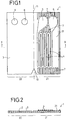
- FIG. 1 is a plan view showing one example of the structure of a heater element (hereinafter called “wafer”) in a unfolded form according to the present invention, which is suitable for use in a tube connecting device.
- FIG. 2 is a cross-sectional view taken along line II - II of FIG. 1.
- a wafer 1 comprises a metal plate 2, an insulation layer 3 formed substantially over the entire internal surface (i.e., the inner surface formed when the metal plate 2 is folded about a bend line 11 to be described later) of the metal plate 2, a resistor 4 which is formed on one surface of the insulation layer 3 which generates heat by electricity, and terminals 5 and 6 having relatively large areas which are respectively electrically connected to both ends of the resistor 4.
- the metal plate 2 is made of a metal having a superior thermal conductivity to allow heat to be uniformly distributed along the surface of the metal.
- An exemplary suitable metal includes, for example, copper, aluminum, gold, silver, iron or alloy including these metals. Of these, copper or copper alloy with a copper content of 99.9% or higher by weight is particularly preferred. This type of metal is preferred because of uniformity of heating and the ease of processing.
- Suitable thickness of the metal plate 2 depends on the material. However, the metal plate 2 may preferably have a thickness range of from 0.08mm to 0.12mm, particularly, 0.95mm to 0.105mm. If the thickness of the metal plate 2 is thicker than these values, then a difficulty in fusing of cut portions of the tubes arises. If, on the other hand, the thickness of the metal plate 2 is thinner than these values, then a difficulty in melting and cutting of the tubes arises.
- the insulation layer 3 formed on the internal surface of the metal plate 2 electrically insulates the resistor 4 from the metal plate 2. Further, the insulation layer 3 serves as an adhesive layer to adhere a half plate 21 of the metal plate 2 on which the resistor is formed (a resistor constitutive portion 21) and another half plate 22 on which no resistor is formed (a resistor non-constitutive portion 22). The two halves 21 and 22 are folded and stuck to each other. Therefore, the insulation layer 3 is required to maintain a desired adhesive force (secondary adhesive force) even after it has been printed, heated and dried.
- materials for the insulation layer 3 may preferably have along with electrical insulating properties, heat-resisting properties (300°C to 350°C), solvent-resisting properties and flow-resisting properties, and may include, for example, epoxy resin, acrylic adhesive, room-temperature hardening type silicone adhesive, polyimide adhesive, polyimide resin, a modified acrylic adhesive, silicone-modified polyimide adhesive, etc.
- the thickness of the insulation layer 3 is set to such a thickness that sufficient insulating properties between the resistor 4 and the metal plate 2 is secured. It may preferably range from 15 ⁇ m to 50 ⁇ m, particularly from 20 ⁇ m to 35 ⁇ m, depending on the materials. If the insulation layer 3 is excessively thick, then it bocomes hard to transfer the heat through the insulation layer 3. If the insulation layer 3 is excessively thin, on the other hand, it becomes hard to obtain a desired thickness of the heater element 1 formed by folding the metal plate 2.
- the insulation layer 3 may be formed, for instance, by applying a liquid including one of the above adhesive materials or their precursors on the internal surface of the metal plate 2 and hardening it.
- the resistor 4 On the insulation layer 3 formed on the resistor constitutive portion 21 side, there are formed the resistor 4 shaped in a desired pattern, the terminals (electrodes) 5 and 6 respectively electrically connected to both ends of the resistor 4, and a plurality of bars 7 arranged in noncontact with the resistor 4 and the terminals 5 and 6, the bars 7 being disposed around the terminals 5 and 6 and on one end of the resistor constitutive portion 21, which is located on the side opposite to the terminals 5 and 6.
- the resistor 4, the terminals 5 and 6 and the bars 7 (hereinafter called generically "resistor 4, etc.") are formed by a screen printing process or formed in a lump if appropriate.
- the resistor 4, etc. may be formed by performing the screen printing process plural times.
- the terminals 5 and 6 may be formed with conductive paste of a different composition.
- Grooves S are respectively defined between the adjacent bars 7.
- the grooves S are provided to discharge gas produced in the insulation layer 3 when the resistor constitutive portion 21 and the resistor non-constitutive portion 22 are bonded together under heat and pressure, along with gas produced in the semi-hardened resistor 4, to the outside. Further, the bars 7 can serve to maintain the thickness of the wafer 1 uniform.
- the conductive paste is printed on the insulation layer 3 of the resistor constitutive portion 21 in a desired pattern by using the screen printing process.
- Conductive substances which are major components of the conductive paste, are normally metallic particles. Among these, silver or silver alloy is particularly preferred.
- silver alloy there may be Ag-Pd alloy, Ag-Pt alloy, Ag-Pd-Pt alloy or the like. Silver alloys containing Pd have excellent migration-resisting properties as compared with pure silver.
- a conductive paste either silver or silver alloy normally exists in the form of particles, in order to increase intervals between the respective particles.
- the average diameter of the particles may preferably range from 0.5 ⁇ m to 50 ⁇ m, particularly, from 1 ⁇ m to 10 ⁇ m. If the average diameter of the particles is less than 0.5 ⁇ m, then the degree of shrinkage of the resistor 4, etc. becomes large. If, on the other hand, the average diameter of the particles is larger than 50 ⁇ m, then the printing properties and the dispersion properties of the conductive paste are lowered.
- Vehicles of a conductive paste may include: binder such as epoxy resin, thermoset melamine resin, acrylic resin, nitrocellulose, ethylcellulose, phenolic resin, vinyl resin or the like; solvent such as butylcarbitol, terpineol or the like; thermoplastic resin such as polyvinyl chloride for improving thermoplasticity; dispersant; activator; viscosity modifier; film adhesive-force accelerating substance (eg, metallic oxide); resistance regulating substance; etc.
- binder such as epoxy resin, thermoset melamine resin, acrylic resin, nitrocellulose, ethylcellulose, phenolic resin, vinyl resin or the like
- solvent such as butylcarbitol, terpineol or the like
- thermoplastic resin such as polyvinyl chloride for improving thermoplasticity
- dispersant activator
- viscosity modifier eg, metallic oxide
- resistance regulating substance etc.
- desired ones can be suitably mixed according to the purpose.
- a conductive paste may contain the vehicles in an amount of from about 10 to 75 wt.%.
- the conductive paste may preferably have a viscosity ranging from 300Ps to 400Ps (at 25°C) from the view point of printing properties and reproducibility of the resistor.
- a screen having a mesh of 180 to 300, particularly, a mesh of 200 to 250 is preferable to employ a screen having a mesh of 180 to 300, particularly, a mesh of 200 to 250.
- the film thickness of the resistor 4, etc. in a hardened state may preferably range from about 10 ⁇ m to 40 ⁇ m, more preferably, about 20 ⁇ m to 30 ⁇ m. This is because a desired heat can be generated.
- the film thickness can be easily set by varying conditions in the screen printing process, such as the thickness of screening emulsion, the rubber hardness of squeegee, an interval between the screen and an object to be printed, the rate of movement of the squeegee, etc.
- the conditions such as the composition, viscosity and film thickness of the conductive paste may differ in each of the resistor 4, the terminals 5 and 6 and the bars 7.
- the conductive paste printed in the predetermined pattern on the insulation layer 3 is dried and hardened using an oven or a hot-air type drier.
- Suitable conditions for drying and hardening the conductive paste may be about 150°C to 200°C in temperature and about 5 to 30 minutes in time.
- the resistance of the so-formed resistor 4 is preferable to set the resistance of the so-formed resistor 4 to range from 8 ⁇ to 16 ⁇ , particularly from 8 ⁇ to 12 ⁇ .
- the number of manufacturing steps, manufacturing time and manufacturing costs can greatly be reduced, even when a complex and fine pattern of the resistor 4, etc. is employed, compared to the conventional etching process of manufacturing the resistor.
- the resistor 4, etc. produced by the screen printing process adhere to the insulation layer 3 firmly enough to prevent the resistor 4, etc. from being peeled off from the insulation layer 3 during production.
- the resistor 4, etc. produced by the screen printing process have excellent heat-resistant properties. Deterioration, such as a crack in the film, is hard to occur even under a rapid temperature change, particularly, under a temperature rise at the time when the resistor constitutive portion 21 and the resistor non-constitutive portion 22 are bonded together under heat and pressure, as described later.
- a main adhesive portion 31 in which the resistor 4, etc. are not formed may preferably be provided on the side (right side as viewed in FIG. 1) opposite to the bend line 11 of the resistor constitutive portion 21.
- a strong adhesive force between the resistor constitutive portion 21 and the resistor non-constitutive portion 22 when they are stucked together can be provided by the main adhesive portion 31.
- the resistor non-constitutive portion 22 has two openings 8 and 9 defined therethrough.
- the openings 8 and 9 are located in positions respectively corresponding to the terminals 5 and 6.
- central portions of the terminals 5 and 6 are exposed through the openings 8 and 9 when the metal plate 2 is folded, to which an electrical source is connected.
- the shape of the openings 8 and 9 is not necessarily limited to the circle shown in FIG. 1. It can be an ellipse, a triangle, a square, a hexagon or the like.
- the metal plate 2 is folded along the bend line 11 so that the resistor 4, etc. are included inside. Simultaneously, the resistor constitutive portion 21 and the resistor non-constitutive portion 22 are stucked together and bonded to each other under heat and pressure to complete the heating element or wafer 1 shown in FIG. 3.
- the heat and pressure conditions in the bonding of the resistor constitutive portion 21 and the resistor non-constitutive portion 22 are decided depending on the materials and thickness of the insulation layer 3. However, a temperature ranging from 170°C to 260°C and a pressure ranging from 5 kg/cm 2 to 40 kg/cm 2 are preferable.
- a cut portion 10 shaped in the form of a triangle, for example, may be provided in the corner of the wafer 1, on the side opposite to where the openings 8 and 9 are and positioned on the bend line 11, as shown in FIG. 3.
- the cut portion 10 serves as a guide in moving the wafer 1.
- the wafer 1 may be manufactured one by one, however, it is more preferable to produce plural wafers at once, from the productivity point of view. In this situation, a plurality of insulation layers 3 and resistors 4 are formed simultaneously on a large metal plate, individual metal plate 2 is cut from the large one, and the openings 8 and 9 are formed in each of them by a punching process, for example.
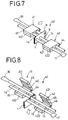
- FIG. 4 is a perspective view showing one example of the structure of a tube connecting device 40.
- FIGS. 5 through 8 are respectively perspective views illustrating steps for connecting tubes 14 and 15 to one another using the tube connecting devices 40.
- the tube connecting devices 40 comprises a set of holders 41 and 42, and a wafer 1 according to the present invention replaceably disposed between the holders.
- Two tubes 14 and 15, made of polyvinyl chloride, for example, are held side by side in the holders 41 and 42, respectively, and melted and cut by the heated wafer 1. While cut ends of the tubes 14 and 15 are in a melted state, one of the holders, 41, is moved, and then the wafer 1 is removed. Thereafter, the melted ends of the tubes 14 and 15 are fused together.
- the holders 41 and 42 respectively comprise holder components 411, 412 and 421, 422 as the upper and lower sides of the respective holders.
- the holder components 411 andg 421 are respectively swingable about supports 44.
- Grooves 45 and 46 each having a semicircular cross-section are respectively provided in the opposing inner surfaces of the holder components 411 and 412.
- the holder components 421 and 422 also have the same grooves.
- a pair of holes 47 and 48 for holding tubes therein are formed in the holder 41 when the holder components 411 and 412 are closed.
- the holes 47 and 48 are formed also in the holder 42.
- a tube clamper (not shown) for pressing and blocking the tube when the holder components 411 and 412 (421 and 422) are closed may be provided inside of each of the holes 47 and 48 of the respective holders.
- the tubes 14 and 15 are laid in parallel for a predetermined length in such a manner that closed ends 16 and 17 of the tubes 14 and 15 directing opposite to each other. Then, the tubes 14 and 15 are respectively inserted into the grooves 45 and 46 of the holders 41 and 42. Thereafter, the holder components 411, 412 and 421, 422 are closed so that the two tubes 14 and 15 are fixedly held by the holes 47 and 48.
- a voltage of 15V to 24V is applied across the terminals 5 and 6 of the wafer 1 by an unillustrated voltage applying means to cause an electric current to flow in the resistor 4 of the wafer 1.
- the resistor 4 generates heat and hence the wafer 1 is heated to a temperature (of about 260°C to 320°C, for example) higher than the melting point of the tubes 14 and 15.
- the tubes 14 and 15 are melted and cut by the heat of the wafer 1. At this time, the cut ends of the tubes 14 and 15 are at a high temperatures under a melted or softened state, and not in communication with the outside since the wafer 1 is in contact with the cut ends, a sterilized state is maintained there.
- the holder 41 While the cut ends of the tubes 14 and 15 are being held in the melted state, the holder 41 is moved in a direction indicated by the arrow in FIG. 7. Thereafter, the holder 41 is stopped and fixed at the position where the sections of the cut tubes 14 and 15 are facing to each other.
- the wafer 1 is pulled out downward as shown in FIG. 8. Thereafter, the holder 41 is pressed toward the holder 42 as necessary. As a result, the sections of the melted tubes 14 and 15 are fused together so that both tubes 14 and 15 are coupled to each other.
- the sections of the tubes 14 and 15 and their peripheral areas are at the high temperature in the melted or softened state. Further, the sections of the tubes contact closely to the surface of the wafer 1 which is maintained at a high temperature, and are hindered from communicating with the outside, until the connection is completed. Thus, the sterilized state of the tubes is perfectly maintained.
- tube members 14' and 15' including the closed ends 16 and 17 are removed to be discarded.
- the used wafer is replaced with a new wafer 1 when other tubes are cut and connected. That is, a disposable or single use of the wafer 1 is preferred in the invention. This necessitates the wafer to provide detectability of whether the wafer is new or not, when it is used.
- the wafer according to the present invention is constructed in such a manner that the resistance of the resistor 4 varies before and after its use.
- Such a wafer may have the same construction as the aforementioned wafer 1 except for the differences which will be described below.
- the conditions (temperature and/or time) of drying and hardening the conductive paste printed to form the resistor 4, etc. on the insulation layer 3 of the wafer 1 are adjusted so that the solvent in the binder of the conductive paste is evaporated to merely solidify the binder.
- the drying and hardening conditions mentioned above should be determined by considering the heat applied when the resistor constitutive component 21 and the resistor non-constitutive component 22 are bonded to each other under heat and pressure after formation of the resistor 4, etc.
- resistor 4 Once such a resistor 4 is energized, it heats itself and the so-solidified binder is further denatured by the heat so that the resistance of the resistor 4 is reduced.
- FIG. 9 is a graph illustrating the manner of variation in the resistance of the resistor 4 with time.
- the graph shows a change in the resistance of the resistor 4 when a dc voltage (of 15V to 20V, for example) is applied across the terminals 5 and 6 of the wafer 1.
- the surface temperature of the wafer 1 is caused to reach 275°C after about 6 seconds, the voltage is then controlled so as to maintain the surface temperature of the wafer 1 at 275°C for 3 seconds, and thereafter the application of the voltage is stopped to cool the wafer 1 down to the room temperature.
- a curve indicative of a variation in the resistance of a resistor 4 in an unused wafer differs from that in a used wafer (indicated by the solid line). That is, the resistance of the resistor 4 in the unused wafer is relatively high throughout the entire process, whereas the resistance in the used wafer is low throughout the entire process, because the binder in the conductive paste is denatured by the heat generated during the use of the wafer.
- Whether the wafer is new or old can be determined by measuring the resistance (or voltage) of the resistor 4 in a predetermined occasion. Thus, the used wafer can be safely avoided from being re-used inadvertently.
- the resistance varying wafer is not necessarily limited to one having the above structure.
- the wafer may have, for example, a structure in which the resistance of the resistor 4 is varied by denaturation of components of the conductive paste such as the conductive substance, the vehicle or the like, or variation in the orientation or linkage states of the components caused by the application of electricity or a temperature change.
- the present invention is not necessarily limited to the structure referred to above.
- the terminals 5 and 6 may be those manufactured by a method other than the screen printing process. Further, the terminals 5 and 6 may be such that are projecting from the outer peripheral edge of the metal plate 2.
- the number of manufacturing steps, manufacturing time and manufacturing costs can greatly be reduced, compared to the conventional etching process of manufacturing the resistor.
- the resistor produced by the screen printing process adheres to the insulation layer strongly enough to prevent the resistor from being peeled off.
- the resistance of the resistor By measuring the resistance of the resistor, it can easily be determined whether the heater element is new or old, since the resistance of the resistor varies before and after the use due to thermal denaturation of binder in the resistor formed of the conductive paste.
- the resistor whose resistance value varies before and after its energization can be manufactured by the screen printing method, for example.
- the resistor can be easily produced by simply controlling the conditions for drying and hardening the conductive paste. It is therefore unnecessary to change a circuit configuration and additionally provide other parts as in the conventional wafer.
- the heater element according to the present invention can be easily manufactured and the manufacturing cost can also be greatly reduced.
Description
Claims (18)
- A heater element (1), to which a predetermined voltage is applied, suitable for use in a tube connecting device, comprising :said resistor (4) comprising a solidified conductive paste applied in a winding pattern on said insulation layer (3), said resistor (4) having first and second ends, said conductive paste including a binder ;a metal plate (2), separated into two halves (21,22) along a fold line (11) ;an insulation layer (3) formed on one surface of said metal plate (2) ;a resistor (4) formed on said insulation layer (3), for electrically generating heat ;
a pair of terminals (5,6) connected to said first and second ends, respectively, of said resistor (4), and a means for applying a voltage across said pair of terminals (5,6) to cause an electrical current to flow through said winding pattern of conductive paste for causing said resistor (4) to generate heat ;
characterized in that the resistance value of said resistor (4) is variable by denaturation of said binder under electrical heating of the resistor itself. - A heater element according to claim 1, wherein said metal plate (2) is made of either copper or copper alloy containing at least 99,9 wt% of copper.
- A heater element according to claim 1 or 2, wherein said metal plate (2) has a thickness ranging from 0.08mm to 0.12mm.
- A heater element according to claim 3, wherein said metal plate (2) has a thickness ranging from 0.09mm to 0.105mm.
- A heater element according to claim 1, wherein the conductive substance of said conductive paste is either silver or a silver alloy.
- A heater element according to claim 5, wherein said silver or silver alloy comprises particles whose average diameter ranges from 0,5µm to 50µm.
- A heater element according to claim 6, wherein said silver or silver alloy comprises particles whose average diameter ranges from 1µm to 10µm.
- A heater element according to claim 1, wherein a plurality of bars (7) and grooves are provided adjacent to said resistor (4) on said insulation layer (3), each of said grooves being respectively defined between two bars, for communicating with an outside of the heater element.
- A heater element according to claim 8, wherein said resistor (4) and said plurality of bars (7) are formed of the same conductive paste.
- A heater element according to claim 8, wherein each of said bars (7) has a film thickness ranging from 10µm to 40µm, after said conductive paste has solidified.
- A heater element according to claim 10, wherein each of said bars (7) has a film thickness ranging from 20µm to 30µm, after said conductive paste has solidified.
- A heater element according to claim 1, wherein an adhesive portion (31) is provided in the vicinity of said resistor (4) on a resistor constitutive portion (21) of said metal plate (2) for bonding said resistor constitutive portion (21) and a resistor non-constitutive portion (22) of said metal plate.
- A heater element according to claim 1, wherein said solidified conductive paste is formed by evaporation of the solvent to solidify the binder.
- A heater element according to claim 1, wherein said resistor (4) has a film thickness ranging from 10µm to 40µm after said conductive paste has solidified.
- A heater element according to claim 1, wherein said resistor (4) has a film thickness ranging from 20µm to 30µm after said conductive paste has solidified.
- A heater element according to claim 1, wherein said insulation layer (3) is made of one material chosen from a group consisting of epoxy resin, acrylic adhesive, silicon adhesive and polyimide adhesive and polyimide resin.
- A heater element according to claim 1, wherein said insulation layer has a thickness ranging from 15µm to 50µm.
- A heater element according to claim 1, wherein said insulation layer has a thickness ranging from 20µm to 35µm.
Applications Claiming Priority (2)
| Application Number | Priority Date | Filing Date | Title |
|---|---|---|---|
| JP15850092A JP3220229B2 (en) | 1992-05-26 | 1992-05-26 | Heating element for tube connection device and method of manufacturing the same |
| JP158500/92 | 1992-05-26 |
Publications (2)
| Publication Number | Publication Date |
|---|---|
| EP0571978A1 EP0571978A1 (en) | 1993-12-01 |
| EP0571978B1 true EP0571978B1 (en) | 1998-04-08 |
Family
ID=15673097
Family Applications (1)
| Application Number | Title | Priority Date | Filing Date |
|---|---|---|---|
| EP19930108501 Expired - Lifetime EP0571978B1 (en) | 1992-05-26 | 1993-05-26 | Heater element for a tube connecting device |
Country Status (5)
| Country | Link |
|---|---|
| US (1) | US5502293A (en) |
| EP (1) | EP0571978B1 (en) |
| JP (1) | JP3220229B2 (en) |
| CA (1) | CA2097049C (en) |
| DE (1) | DE69317812T2 (en) |
Families Citing this family (28)
| Publication number | Priority date | Publication date | Assignee | Title |
|---|---|---|---|---|
| JP3377879B2 (en) * | 1995-03-02 | 2003-02-17 | 松下電器産業株式会社 | Heated cutting blade |
| JP3422452B2 (en) * | 1995-12-08 | 2003-06-30 | テルモ株式会社 | Tube connection device |
| US5657532A (en) * | 1996-01-16 | 1997-08-19 | Ferro Corporation | Method of making insulated electrical heating element using LTCC tape |
| US6752777B1 (en) | 1997-06-16 | 2004-06-22 | Terumo Kabushiki Kaisha | Blood component collecting apparatus |
| WO1999030536A1 (en) * | 1997-12-05 | 1999-06-17 | Koninklijke Philips Electronics N.V. | Immersion heating element |
| US6111233A (en) * | 1999-01-13 | 2000-08-29 | Malden Mills Industries, Inc. | Electric heating warming fabric articles |
| US6132833A (en) * | 1999-04-06 | 2000-10-17 | Denco | Wafer for use in selective connecting and disconnecting of plastic tubes |
| US6852956B2 (en) | 1999-04-22 | 2005-02-08 | Malden Mills Industries, Inc. | Fabric with heated circuit printed on intermediate film |
| US6875963B2 (en) | 1999-04-23 | 2005-04-05 | Malden Mills Industries, Inc. | Electric heating/warming fabric articles |
| FR2803010B1 (en) * | 1999-12-24 | 2002-02-01 | Aventis Pasteur | METHOD AND APPARATUS FOR STERILE CONNECTION OF TWO FLEXIBLE TUBES |
| NL1014620C2 (en) * | 2000-03-13 | 2001-09-14 | Inventum B V | Heating element and method of manufacturing it. |
| US7777156B2 (en) | 2002-01-14 | 2010-08-17 | Mmi-Ipco, Llc | Electric heating/warming fabric articles |
| US7268320B2 (en) | 2002-01-14 | 2007-09-11 | Mmi-Ipco, Llc | Electric heating/warming fabric articles |
| US7202443B2 (en) | 2002-01-14 | 2007-04-10 | Malden Mills Industries, Inc. | Electric heating/warming fabric articles |
| AT7326U1 (en) * | 2003-12-04 | 2005-01-25 | Econ Exp & Consulting Group Gm | METHOD FOR PRODUCING A FLAT HEATING ELEMENT AND PRODUCED FLOOR HEATING ELEMENT THEREOF |
| SE0303416L (en) * | 2003-12-18 | 2005-06-19 | Gambro Lundia Ab | Packaging intended for use in a peritoneal dialysis treatment and process for making such a package |
| FR2904615B1 (en) * | 2006-08-03 | 2008-09-12 | Solystic Sas | METHOD FOR CONTROLLING THE VOLTAGE OF A CARROUSEL CHAIN WITH GODETS |
| US8592730B2 (en) * | 2006-12-20 | 2013-11-26 | Tomier, Inc. | Heater assembly for suture welder |
| JP5773723B2 (en) * | 2011-04-20 | 2015-09-02 | 株式会社アワジテック | Moisture sensor |
| RU2478480C1 (en) * | 2012-03-19 | 2013-04-10 | Открытое акционерное общество "Научно-исследовательский институт "Кулон" | Laminar plate of device for sterile bonding (welding) of polymer ducts from thermosetting materials of polymer containers |
| CN104189967B (en) * | 2014-09-11 | 2017-02-22 | 昆山韦睿医疗科技有限公司 | Heater detection method and peritoneal dialysis equipment |
| CN106233818B (en) | 2015-04-07 | 2020-10-27 | 源鉴定私人有限公司 | Direct current heater |
| IT201800009120A1 (en) * | 2018-10-03 | 2020-04-03 | Gd Sp:A | Welder device and method for its realization. |
| GB2582166A (en) * | 2019-03-13 | 2020-09-16 | Green Light Packaging Ltd | Film-closure apparatus for plastic film material |
| SG10202002436XA (en) * | 2020-03-17 | 2021-10-28 | Racer Tech Pte Ltd | Electromechanical Sterile Tube Connecting Devices |
| CN114789561A (en) | 2021-01-25 | 2022-07-26 | 汾沃有限公司 | Aseptic connection of tubes |
| RU2768713C1 (en) * | 2021-04-20 | 2022-03-24 | Общество с ограниченной ответственностью "ПРОФИТ ФАРМ" | Heater plate for sterile connection of plastic lines |
| WO2024069835A1 (en) | 2022-09-29 | 2024-04-04 | Terumo Kabushiki Kaisha | Fusion bonding wafer, tube fusion bonding device, and tube fusion bonding method |
Family Cites Families (24)
| Publication number | Priority date | Publication date | Assignee | Title |
|---|---|---|---|---|
| US2859321A (en) * | 1955-07-11 | 1958-11-04 | Garaway Alexander | Electric resistance heater |
| US2939807A (en) * | 1956-06-29 | 1960-06-07 | Thermway Ind Inc | Method of making a heating panel |
| US3830656A (en) * | 1967-11-15 | 1974-08-20 | T Okiyama | Resistor film |
| US3833410A (en) * | 1971-12-30 | 1974-09-03 | Trw Inc | High stability thin film alloy resistors |
| DE2329424A1 (en) * | 1973-06-08 | 1975-01-02 | Siemens Ag | Flat printed circuit heating element - comprises refractory plate sandwich |
| US3944787A (en) * | 1973-12-26 | 1976-03-16 | Texas Instruments Incorporated | Heater on metal composites |
| US3934119A (en) * | 1974-09-17 | 1976-01-20 | Texas Instruments Incorporated | Electrical resistance heaters |
| US4130671A (en) * | 1977-09-30 | 1978-12-19 | The United States Of America As Represented By The United States Department Of Energy | Method for preparing a thick film conductor |
| DE2916329C3 (en) * | 1979-04-23 | 1982-03-11 | Siemens AG, 1000 Berlin und 8000 München | Electrical network |
| NL8102809A (en) * | 1981-06-11 | 1983-01-03 | Philips Nv | RESISTANCE PASTE FOR A RESISTANCE BODY. |
| JPS58148493A (en) * | 1982-03-01 | 1983-09-03 | アルプス電気株式会社 | Paste for forming transparent conductive film |
| US4507119A (en) * | 1982-07-06 | 1985-03-26 | E. I. Du Pont De Nemours And Company | Sterile docking process, apparatus and system |
| US4501951A (en) * | 1982-08-16 | 1985-02-26 | E. I. Du Pont De Nemours And Company | Electric heating element for sterilely cutting and welding together thermoplastic tubes |
| US4647756A (en) * | 1983-07-05 | 1987-03-03 | E. I. Du Pont De Nemours And Company | Electrical resistance heating element with signal means to indicate first use |
| DE3409925A1 (en) * | 1984-03-17 | 1985-09-26 | Robert Krups Stiftung & Co KG, 5650 Solingen | RADIATOR FOR HOUSEHOLD APPLIANCES |
| JPS6130582A (en) * | 1984-07-20 | 1986-02-12 | Sanyo Kokusaku Pulp Co Ltd | 2,6-dibromo-4-n-alkylphenyl-glycidyl ether and its preparation |
| US4633063A (en) * | 1984-12-27 | 1986-12-30 | E. I. Du Pont De Nemours And Company | Vented heating element for sterile cutting and welding together of thermoplastic tubes |
| US4864101A (en) * | 1987-01-09 | 1989-09-05 | Denco, Inc. | Hybrid welding wafer |
| GB8704468D0 (en) * | 1987-02-25 | 1987-04-01 | Thorn Emi Appliances | Substrates for supporting electrical components |
| GB8818104D0 (en) * | 1988-07-29 | 1988-09-01 | Emaco Ltd | Improvements in & relating to cooking appliances |
| US5096619A (en) * | 1989-03-23 | 1992-03-17 | E. I. Du Pont De Nemours And Company | Thick film low-end resistor composition |
| US5155800A (en) * | 1991-02-27 | 1992-10-13 | Process Technology Inc. | Panel heater assembly for use in a corrosive environment and method of manufacturing the heater |
| US5252944A (en) * | 1991-09-12 | 1993-10-12 | Caddock Electronics, Inc. | Film-type electrical resistor combination |
| US5221644A (en) * | 1991-12-13 | 1993-06-22 | Delco Electronics Corporation | Thick film sense resistor composition and method of using the same |
-
1992
- 1992-05-26 JP JP15850092A patent/JP3220229B2/en not_active Expired - Lifetime
-
1993
- 1993-05-25 US US08/066,430 patent/US5502293A/en not_active Expired - Lifetime
- 1993-05-26 DE DE1993617812 patent/DE69317812T2/en not_active Expired - Lifetime
- 1993-05-26 CA CA 2097049 patent/CA2097049C/en not_active Expired - Lifetime
- 1993-05-26 EP EP19930108501 patent/EP0571978B1/en not_active Expired - Lifetime
Also Published As
| Publication number | Publication date |
|---|---|
| JP3220229B2 (en) | 2001-10-22 |
| JPH05326117A (en) | 1993-12-10 |
| DE69317812T2 (en) | 1998-08-27 |
| US5502293A (en) | 1996-03-26 |
| EP0571978A1 (en) | 1993-12-01 |
| DE69317812D1 (en) | 1998-05-14 |
| CA2097049C (en) | 1997-11-11 |
| CA2097049A1 (en) | 1993-11-27 |
Similar Documents
| Publication | Publication Date | Title |
|---|---|---|
| EP0571978B1 (en) | Heater element for a tube connecting device | |
| US4501951A (en) | Electric heating element for sterilely cutting and welding together thermoplastic tubes | |
| US5351390A (en) | Manufacturing method for a PTC thermistor | |
| US4647756A (en) | Electrical resistance heating element with signal means to indicate first use | |
| US5039844A (en) | PTC devices and their preparation | |
| US4330704A (en) | Electrical devices comprising conductive polymers | |
| US5065501A (en) | Generating electromagnetic fields in a self regulating temperature heater by positioning of a current return bus | |
| KR20140089419A (en) | Heater, and fixing device and drying device provided with same | |
| US4517449A (en) | Laminar electrical heaters | |
| US4633063A (en) | Vented heating element for sterile cutting and welding together of thermoplastic tubes | |
| JP3377879B2 (en) | Heated cutting blade | |
| JPH10502762A (en) | Method for forming a conductive connection | |
| JPS6134235B2 (en) | ||
| JP4865968B2 (en) | Contact heating element | |
| JPS62181900A (en) | Method and device for thermally separating multilayer film | |
| JPH0387001A (en) | Ptc thermistor and manufacture thereof | |
| CN113756915B (en) | Electrically heated catalyst device, method for producing same, and metal sheet for electrode of electrically heated catalyst device | |
| RU2768713C1 (en) | Heater plate for sterile connection of plastic lines | |
| JP3678882B2 (en) | Ceramic heater | |
| JPH03129694A (en) | Heating element | |
| JPH09246013A (en) | Chip ptc thermistor | |
| JP2745538B2 (en) | Electric joining method between ceramics and insert material for joining | |
| JPS60184836A (en) | Laminated conductive polymer device | |
| JPS6242460Y2 (en) | ||
| JPH046787A (en) | Planar heater |
Legal Events
| Date | Code | Title | Description |
|---|---|---|---|
| PUAI | Public reference made under article 153(3) epc to a published international application that has entered the european phase |
Free format text: ORIGINAL CODE: 0009012 |
|
| 17P | Request for examination filed |
Effective date: 19930526 |
|
| AK | Designated contracting states |
Kind code of ref document: A1 Designated state(s): BE DE FR GB IT NL SE |
|
| 17Q | First examination report despatched |
Effective date: 19960725 |
|
| GRAG | Despatch of communication of intention to grant |
Free format text: ORIGINAL CODE: EPIDOS AGRA |
|
| GRAG | Despatch of communication of intention to grant |
Free format text: ORIGINAL CODE: EPIDOS AGRA |
|
| GRAG | Despatch of communication of intention to grant |
Free format text: ORIGINAL CODE: EPIDOS AGRA |
|
| GRAH | Despatch of communication of intention to grant a patent |
Free format text: ORIGINAL CODE: EPIDOS IGRA |
|
| GRAH | Despatch of communication of intention to grant a patent |
Free format text: ORIGINAL CODE: EPIDOS IGRA |
|
| GRAA | (expected) grant |
Free format text: ORIGINAL CODE: 0009210 |
|
| AK | Designated contracting states |
Kind code of ref document: B1 Designated state(s): BE DE FR GB IT NL SE |
|
| ITF | It: translation for a ep patent filed |
Owner name: FUMERO BREVETTI S.N.C. |
|
| REF | Corresponds to: |
Ref document number: 69317812 Country of ref document: DE Date of ref document: 19980514 |
|
| ET | Fr: translation filed | ||
| PLBE | No opposition filed within time limit |
Free format text: ORIGINAL CODE: 0009261 |
|
| STAA | Information on the status of an ep patent application or granted ep patent |
Free format text: STATUS: NO OPPOSITION FILED WITHIN TIME LIMIT |
|
| 26N | No opposition filed | ||
| REG | Reference to a national code |
Ref country code: GB Ref legal event code: IF02 |
|
| PGFP | Annual fee paid to national office [announced via postgrant information from national office to epo] |
Ref country code: NL Payment date: 20120523 Year of fee payment: 20 Ref country code: DE Payment date: 20120523 Year of fee payment: 20 |
|
| PGFP | Annual fee paid to national office [announced via postgrant information from national office to epo] |
Ref country code: GB Payment date: 20120523 Year of fee payment: 20 Ref country code: BE Payment date: 20120514 Year of fee payment: 20 Ref country code: SE Payment date: 20120511 Year of fee payment: 20 Ref country code: FR Payment date: 20120608 Year of fee payment: 20 |
|
| PGFP | Annual fee paid to national office [announced via postgrant information from national office to epo] |
Ref country code: IT Payment date: 20120518 Year of fee payment: 20 |
|
| REG | Reference to a national code |
Ref country code: DE Ref legal event code: R071 Ref document number: 69317812 Country of ref document: DE |
|
| BE20 | Be: patent expired |
Owner name: *TERUMO K.K. Effective date: 20130526 |
|
| REG | Reference to a national code |
Ref country code: NL Ref legal event code: V4 Effective date: 20130526 |
|
| REG | Reference to a national code |
Ref country code: GB Ref legal event code: PE20 Expiry date: 20130525 |
|
| PG25 | Lapsed in a contracting state [announced via postgrant information from national office to epo] |
Ref country code: GB Free format text: LAPSE BECAUSE OF EXPIRATION OF PROTECTION Effective date: 20130525 Ref country code: DE Free format text: LAPSE BECAUSE OF EXPIRATION OF PROTECTION Effective date: 20130528 |